KR20150125580A - 발광 소자, 발광 장치, 조명 장치, 전자 기기 - Google Patents
발광 소자, 발광 장치, 조명 장치, 전자 기기 Download PDFInfo
- Publication number
- KR20150125580A KR20150125580A KR1020150054650A KR20150054650A KR20150125580A KR 20150125580 A KR20150125580 A KR 20150125580A KR 1020150054650 A KR1020150054650 A KR 1020150054650A KR 20150054650 A KR20150054650 A KR 20150054650A KR 20150125580 A KR20150125580 A KR 20150125580A
- Authority
- KR
- South Korea
- Prior art keywords
- layer
- light emitting
- cathode
- light
- emitting device
- Prior art date
- Legal status (The legal status is an assumption and is not a legal conclusion. Google has not performed a legal analysis and makes no representation as to the accuracy of the status listed.)
- Ceased
Links
Images


Classifications
-
- H—ELECTRICITY
- H10—SEMICONDUCTOR DEVICES; ELECTRIC SOLID-STATE DEVICES NOT OTHERWISE PROVIDED FOR
- H10K—ORGANIC ELECTRIC SOLID-STATE DEVICES
- H10K59/00—Integrated devices, or assemblies of multiple devices, comprising at least one organic light-emitting element covered by group H10K50/00
- H10K59/30—Devices specially adapted for multicolour light emission
- H10K59/38—Devices specially adapted for multicolour light emission comprising colour filters or colour changing media [CCM]
-
- H01L51/5296—
-
- H—ELECTRICITY
- H10—SEMICONDUCTOR DEVICES; ELECTRIC SOLID-STATE DEVICES NOT OTHERWISE PROVIDED FOR
- H10D—INORGANIC ELECTRIC SEMICONDUCTOR DEVICES
- H10D30/00—Field-effect transistors [FET]
- H10D30/60—Insulated-gate field-effect transistors [IGFET]
- H10D30/67—Thin-film transistors [TFT]
-
- H01L51/0072—
-
- H01L51/506—
-
- H01L51/5076—
-
- H01L51/5206—
-
- H01L51/5221—
-
- H01L51/5278—
-
- H—ELECTRICITY
- H10—SEMICONDUCTOR DEVICES; ELECTRIC SOLID-STATE DEVICES NOT OTHERWISE PROVIDED FOR
- H10D—INORGANIC ELECTRIC SEMICONDUCTOR DEVICES
- H10D30/00—Field-effect transistors [FET]
- H10D30/60—Insulated-gate field-effect transistors [IGFET]
- H10D30/67—Thin-film transistors [TFT]
- H10D30/674—Thin-film transistors [TFT] characterised by the active materials
- H10D30/6755—Oxide semiconductors, e.g. zinc oxide, copper aluminium oxide or cadmium stannate
-
- H—ELECTRICITY
- H10—SEMICONDUCTOR DEVICES; ELECTRIC SOLID-STATE DEVICES NOT OTHERWISE PROVIDED FOR
- H10D—INORGANIC ELECTRIC SEMICONDUCTOR DEVICES
- H10D62/00—Semiconductor bodies, or regions thereof, of devices having potential barriers
- H10D62/80—Semiconductor bodies, or regions thereof, of devices having potential barriers characterised by the materials
-
- H—ELECTRICITY
- H10—SEMICONDUCTOR DEVICES; ELECTRIC SOLID-STATE DEVICES NOT OTHERWISE PROVIDED FOR
- H10D—INORGANIC ELECTRIC SEMICONDUCTOR DEVICES
- H10D62/00—Semiconductor bodies, or regions thereof, of devices having potential barriers
- H10D62/80—Semiconductor bodies, or regions thereof, of devices having potential barriers characterised by the materials
- H10D62/875—Semiconductor bodies, or regions thereof, of devices having potential barriers characterised by the materials being semiconductor metal oxide, e.g. InGaZnO
-
- H—ELECTRICITY
- H10—SEMICONDUCTOR DEVICES; ELECTRIC SOLID-STATE DEVICES NOT OTHERWISE PROVIDED FOR
- H10D—INORGANIC ELECTRIC SEMICONDUCTOR DEVICES
- H10D86/00—Integrated devices formed in or on insulating or conducting substrates, e.g. formed in silicon-on-insulator [SOI] substrates or on stainless steel or glass substrates
- H10D86/40—Integrated devices formed in or on insulating or conducting substrates, e.g. formed in silicon-on-insulator [SOI] substrates or on stainless steel or glass substrates characterised by multiple TFTs
- H10D86/421—Integrated devices formed in or on insulating or conducting substrates, e.g. formed in silicon-on-insulator [SOI] substrates or on stainless steel or glass substrates characterised by multiple TFTs having a particular composition, shape or crystalline structure of the active layer
- H10D86/423—Integrated devices formed in or on insulating or conducting substrates, e.g. formed in silicon-on-insulator [SOI] substrates or on stainless steel or glass substrates characterised by multiple TFTs having a particular composition, shape or crystalline structure of the active layer comprising semiconductor materials not belonging to the Group IV, e.g. InGaZnO
-
- H—ELECTRICITY
- H10—SEMICONDUCTOR DEVICES; ELECTRIC SOLID-STATE DEVICES NOT OTHERWISE PROVIDED FOR
- H10D—INORGANIC ELECTRIC SEMICONDUCTOR DEVICES
- H10D86/00—Integrated devices formed in or on insulating or conducting substrates, e.g. formed in silicon-on-insulator [SOI] substrates or on stainless steel or glass substrates
- H10D86/40—Integrated devices formed in or on insulating or conducting substrates, e.g. formed in silicon-on-insulator [SOI] substrates or on stainless steel or glass substrates characterised by multiple TFTs
- H10D86/60—Integrated devices formed in or on insulating or conducting substrates, e.g. formed in silicon-on-insulator [SOI] substrates or on stainless steel or glass substrates characterised by multiple TFTs wherein the TFTs are in active matrices
-
- H—ELECTRICITY
- H10—SEMICONDUCTOR DEVICES; ELECTRIC SOLID-STATE DEVICES NOT OTHERWISE PROVIDED FOR
- H10K—ORGANIC ELECTRIC SOLID-STATE DEVICES
- H10K50/00—Organic light-emitting devices
- H10K50/10—OLEDs or polymer light-emitting diodes [PLED]
- H10K50/11—OLEDs or polymer light-emitting diodes [PLED] characterised by the electroluminescent [EL] layers
-
- H—ELECTRICITY
- H10—SEMICONDUCTOR DEVICES; ELECTRIC SOLID-STATE DEVICES NOT OTHERWISE PROVIDED FOR
- H10K—ORGANIC ELECTRIC SOLID-STATE DEVICES
- H10K50/00—Organic light-emitting devices
- H10K50/10—OLEDs or polymer light-emitting diodes [PLED]
- H10K50/14—Carrier transporting layers
- H10K50/16—Electron transporting layers
-
- H—ELECTRICITY
- H10—SEMICONDUCTOR DEVICES; ELECTRIC SOLID-STATE DEVICES NOT OTHERWISE PROVIDED FOR
- H10K—ORGANIC ELECTRIC SOLID-STATE DEVICES
- H10K50/00—Organic light-emitting devices
- H10K50/10—OLEDs or polymer light-emitting diodes [PLED]
- H10K50/17—Carrier injection layers
- H10K50/171—Electron injection layers
-
- H—ELECTRICITY
- H10—SEMICONDUCTOR DEVICES; ELECTRIC SOLID-STATE DEVICES NOT OTHERWISE PROVIDED FOR
- H10K—ORGANIC ELECTRIC SOLID-STATE DEVICES
- H10K50/00—Organic light-emitting devices
- H10K50/80—Constructional details
- H10K50/805—Electrodes
- H10K50/81—Anodes
-
- H—ELECTRICITY
- H10—SEMICONDUCTOR DEVICES; ELECTRIC SOLID-STATE DEVICES NOT OTHERWISE PROVIDED FOR
- H10K—ORGANIC ELECTRIC SOLID-STATE DEVICES
- H10K50/00—Organic light-emitting devices
- H10K50/80—Constructional details
- H10K50/805—Electrodes
- H10K50/82—Cathodes
- H10K50/828—Transparent cathodes, e.g. comprising thin metal layers
-
- H—ELECTRICITY
- H10—SEMICONDUCTOR DEVICES; ELECTRIC SOLID-STATE DEVICES NOT OTHERWISE PROVIDED FOR
- H10K—ORGANIC ELECTRIC SOLID-STATE DEVICES
- H10K59/00—Integrated devices, or assemblies of multiple devices, comprising at least one organic light-emitting element covered by group H10K50/00
- H10K59/10—OLED displays
- H10K59/12—Active-matrix OLED [AMOLED] displays
- H10K59/123—Connection of the pixel electrodes to the thin film transistors [TFT]
-
- H—ELECTRICITY
- H10—SEMICONDUCTOR DEVICES; ELECTRIC SOLID-STATE DEVICES NOT OTHERWISE PROVIDED FOR
- H10K—ORGANIC ELECTRIC SOLID-STATE DEVICES
- H10K59/00—Integrated devices, or assemblies of multiple devices, comprising at least one organic light-emitting element covered by group H10K50/00
- H10K59/40—OLEDs integrated with touch screens
-
- H—ELECTRICITY
- H10—SEMICONDUCTOR DEVICES; ELECTRIC SOLID-STATE DEVICES NOT OTHERWISE PROVIDED FOR
- H10K—ORGANIC ELECTRIC SOLID-STATE DEVICES
- H10K59/00—Integrated devices, or assemblies of multiple devices, comprising at least one organic light-emitting element covered by group H10K50/00
- H10K59/80—Constructional details
- H10K59/805—Electrodes
- H10K59/8051—Anodes
-
- H—ELECTRICITY
- H10—SEMICONDUCTOR DEVICES; ELECTRIC SOLID-STATE DEVICES NOT OTHERWISE PROVIDED FOR
- H10K—ORGANIC ELECTRIC SOLID-STATE DEVICES
- H10K59/00—Integrated devices, or assemblies of multiple devices, comprising at least one organic light-emitting element covered by group H10K50/00
- H10K59/80—Constructional details
- H10K59/805—Electrodes
- H10K59/8052—Cathodes
-
- H—ELECTRICITY
- H10—SEMICONDUCTOR DEVICES; ELECTRIC SOLID-STATE DEVICES NOT OTHERWISE PROVIDED FOR
- H10K—ORGANIC ELECTRIC SOLID-STATE DEVICES
- H10K85/00—Organic materials used in the body or electrodes of devices covered by this subclass
- H10K85/60—Organic compounds having low molecular weight
- H10K85/649—Aromatic compounds comprising a hetero atom
- H10K85/654—Aromatic compounds comprising a hetero atom comprising only nitrogen as heteroatom
-
- H—ELECTRICITY
- H10—SEMICONDUCTOR DEVICES; ELECTRIC SOLID-STATE DEVICES NOT OTHERWISE PROVIDED FOR
- H10K—ORGANIC ELECTRIC SOLID-STATE DEVICES
- H10K85/00—Organic materials used in the body or electrodes of devices covered by this subclass
- H10K85/60—Organic compounds having low molecular weight
- H10K85/649—Aromatic compounds comprising a hetero atom
- H10K85/657—Polycyclic condensed heteroaromatic hydrocarbons
-
- H01L2924/01101—
-
- H01L2924/01102—
-
- H01L2924/12044—
-
- H—ELECTRICITY
- H10—SEMICONDUCTOR DEVICES; ELECTRIC SOLID-STATE DEVICES NOT OTHERWISE PROVIDED FOR
- H10K—ORGANIC ELECTRIC SOLID-STATE DEVICES
- H10K2102/00—Constructional details relating to the organic devices covered by this subclass
-
- H—ELECTRICITY
- H10—SEMICONDUCTOR DEVICES; ELECTRIC SOLID-STATE DEVICES NOT OTHERWISE PROVIDED FOR
- H10K—ORGANIC ELECTRIC SOLID-STATE DEVICES
- H10K2102/00—Constructional details relating to the organic devices covered by this subclass
- H10K2102/10—Transparent electrodes, e.g. using graphene
- H10K2102/101—Transparent electrodes, e.g. using graphene comprising transparent conductive oxides [TCO]
- H10K2102/102—Transparent electrodes, e.g. using graphene comprising transparent conductive oxides [TCO] comprising tin oxides, e.g. fluorine-doped SnO2
-
- H—ELECTRICITY
- H10—SEMICONDUCTOR DEVICES; ELECTRIC SOLID-STATE DEVICES NOT OTHERWISE PROVIDED FOR
- H10K—ORGANIC ELECTRIC SOLID-STATE DEVICES
- H10K2102/00—Constructional details relating to the organic devices covered by this subclass
- H10K2102/10—Transparent electrodes, e.g. using graphene
- H10K2102/101—Transparent electrodes, e.g. using graphene comprising transparent conductive oxides [TCO]
- H10K2102/103—Transparent electrodes, e.g. using graphene comprising transparent conductive oxides [TCO] comprising indium oxides, e.g. ITO
-
- H—ELECTRICITY
- H10—SEMICONDUCTOR DEVICES; ELECTRIC SOLID-STATE DEVICES NOT OTHERWISE PROVIDED FOR
- H10K—ORGANIC ELECTRIC SOLID-STATE DEVICES
- H10K2102/00—Constructional details relating to the organic devices covered by this subclass
- H10K2102/301—Details of OLEDs
- H10K2102/321—Inverted OLED, i.e. having cathode between substrate and anode
-
- H—ELECTRICITY
- H10—SEMICONDUCTOR DEVICES; ELECTRIC SOLID-STATE DEVICES NOT OTHERWISE PROVIDED FOR
- H10K—ORGANIC ELECTRIC SOLID-STATE DEVICES
- H10K85/00—Organic materials used in the body or electrodes of devices covered by this subclass
- H10K85/30—Coordination compounds
- H10K85/341—Transition metal complexes, e.g. Ru(II)polypyridine complexes
- H10K85/342—Transition metal complexes, e.g. Ru(II)polypyridine complexes comprising iridium
-
- H—ELECTRICITY
- H10—SEMICONDUCTOR DEVICES; ELECTRIC SOLID-STATE DEVICES NOT OTHERWISE PROVIDED FOR
- H10K—ORGANIC ELECTRIC SOLID-STATE DEVICES
- H10K85/00—Organic materials used in the body or electrodes of devices covered by this subclass
- H10K85/60—Organic compounds having low molecular weight
- H10K85/615—Polycyclic condensed aromatic hydrocarbons, e.g. anthracene
-
- H—ELECTRICITY
- H10—SEMICONDUCTOR DEVICES; ELECTRIC SOLID-STATE DEVICES NOT OTHERWISE PROVIDED FOR
- H10K—ORGANIC ELECTRIC SOLID-STATE DEVICES
- H10K85/00—Organic materials used in the body or electrodes of devices covered by this subclass
- H10K85/60—Organic compounds having low molecular weight
- H10K85/631—Amine compounds having at least two aryl rest on at least one amine-nitrogen atom, e.g. triphenylamine
-
- H—ELECTRICITY
- H10—SEMICONDUCTOR DEVICES; ELECTRIC SOLID-STATE DEVICES NOT OTHERWISE PROVIDED FOR
- H10K—ORGANIC ELECTRIC SOLID-STATE DEVICES
- H10K85/00—Organic materials used in the body or electrodes of devices covered by this subclass
- H10K85/60—Organic compounds having low molecular weight
- H10K85/649—Aromatic compounds comprising a hetero atom
- H10K85/657—Polycyclic condensed heteroaromatic hydrocarbons
- H10K85/6572—Polycyclic condensed heteroaromatic hydrocarbons comprising only nitrogen in the heteroaromatic polycondensed ring system, e.g. phenanthroline or carbazole
-
- H—ELECTRICITY
- H10—SEMICONDUCTOR DEVICES; ELECTRIC SOLID-STATE DEVICES NOT OTHERWISE PROVIDED FOR
- H10K—ORGANIC ELECTRIC SOLID-STATE DEVICES
- H10K85/00—Organic materials used in the body or electrodes of devices covered by this subclass
- H10K85/60—Organic compounds having low molecular weight
- H10K85/649—Aromatic compounds comprising a hetero atom
- H10K85/657—Polycyclic condensed heteroaromatic hydrocarbons
- H10K85/6576—Polycyclic condensed heteroaromatic hydrocarbons comprising only sulfur in the heteroaromatic polycondensed ring system, e.g. benzothiophene
Landscapes
- Physics & Mathematics (AREA)
- Optics & Photonics (AREA)
- Engineering & Computer Science (AREA)
- Microelectronics & Electronic Packaging (AREA)
- Spectroscopy & Molecular Physics (AREA)
- Chemical & Material Sciences (AREA)
- Materials Engineering (AREA)
- Electroluminescent Light Sources (AREA)
- Optical Filters (AREA)
Abstract
본 명세서에서 개시(開示)하는 발명의 일 형태의 구성은 음극, 음극 위의 제 1 층, 제 1 층 위의 제 2 층, 제 2 층 위의 발광층, 및 발광층 위의 양극을 포함하고, 제 2 층은 알칼리 금속 또는 알칼리 토금속을 함유하고, 제 1 층은 전자 수송성 재료를 함유하는, 발광 소자이다. 역구조의 발광 소자에 있어서, 전자 주입층의 재료에 함유되는 알칼리 금속 또는 알칼리 토금속이, 먼저 형성된 음극과 접촉하면, EL 소자의 구동 전압의 상승이나 발광 효율 저하를 초래한다. 특히 음극이 산화물 도전막을 함유하고 있으면, 문제는 현저해진다. 이를 방지하기 위하여, 음극과 전자 주입층 사이에 버퍼가 되는 층을 제공한다.
Description
도 2는 발광 소자의 구조에 대하여 설명하기 위한 도면.
도 3은 발광 장치에 대하여 설명하기 위한 도면.
도 4는 전자 기기에 대하여 설명하기 위한 도면.
도 5는 전자 기기에 대하여 설명하기 위한 도면.
도 6은 조명 장치에 대하여 설명하기 위한 도면.
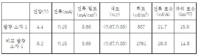
도 7은 발광 소자 1 및 비교 발광 소자 1의 휘도-전류 효율 특성을 나타낸 그래프.
도 8은 발광 소자 1 및 비교 발광 소자 1의 전압-전류 특성을 나타낸 그래프.
도 9는 발광 소자 1 및 비교 발광 소자 1의 정규화 휘도의 시간 변화를 나타낸 그래프.
도 10은 발광 소자 2 및 비교 발광 소자 2의 휘도-전류 효율 특성을 나타낸 그래프.
도 11은 발광 소자 2 및 비교 발광 소자 2의 전압-전류 특성을 나타낸 그래프.
도 12는 발광 소자 2 및 비교 발광 소자 2의 정규화 휘도의 시간 변화를 나타낸 그래프.
도 13은 본 발명의 일 형태에 따른 발광 장치를 설명하기 위한 도면.
도 14는 본 발명의 일 형태에 따른 발광 장치를 설명하기 위한 도면.
도 15는 본 발명의 일 형태에 따른 조명 장치를 설명하기 위한 도면.
도 16은 터치 센서를 설명하기 위한 도면.
도 17은 터치 센서를 설명하기 위한 회로도.
도 18은 터치 센서를 설명하기 위한 단면도.
도 19는 본 발명의 일 형태에 따른 발광 장치를 사용한 모듈을 설명하기 위한 도면.
도 20은 본 발명의 일 형태에 따른 발광 소자를 설명하기 위한 도면.
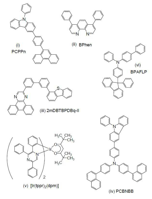

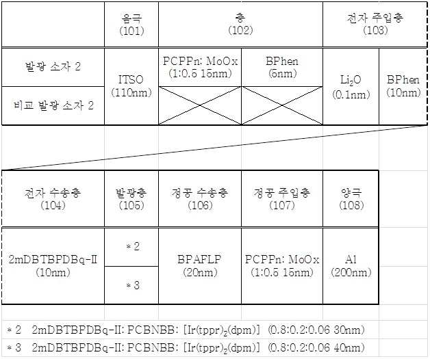

101: 음극
102: 층
103: 전자 주입층
104: 전자 수송층
105: 발광층
106: 정공 수송층
107: 정공 주입층
108: 양극
200: 기판
201: 음극
202: 층
203: EL층
205: 양극
204: 중간층
501: 소자 기판
502: 화소부
503: 구동 회로부(소스선 구동 회로)
504a, 504b: 구동 회로부(게이트선 구동 회로)
505: 밀봉재
506: 밀봉 기판
507: 배선
508: FPC
509: n채널형 FET
510: p채널형 FET
511: 스위칭 FET
512: 전류 제어용 FET
513: 음극
514: 절연물
515: EL층
516: 양극
519: 발광 소자
520: 공간
2001: 제 1 기판
2002: 발광부
2005a: 제 1 밀봉재
2005b: 제 2 밀봉재
2006: 제 2 기판
2011: 제 2 공간
2013: 제 1 공간
3100: 발광 장치
3101: 기판
3103a: 하부 전극
3103b: 하부 전극
3103c: 하부 전극
3105a: 투명 도전막
3105b: 투명 도전막
3107a: 격벽
3107b: 격벽
3107c: 격벽
3107d: 격벽
3110: 층
3112: 전자 주입층
3113: 전자 수송층
3114: 발광층
3116: 정공 수송층
3118: 정공 주입층
3119: 상부 전극
3120a: 발광 소자
3120b: 발광 소자
3120c: 발광 소자
4000: 조명 장치
4001: 조명 장치
4003: 기판
4005: 기판
4007: 발광 소자
4009: 전극
4011: 전극
4013: 하부 전극
4014: EL층
4015: 상부 전극
4017: 보조 배선
4019: 밀봉 기판
4021: 밀봉재
4023: 건조제
4025: 기판
4027: 확산판
4100: 조명 장치
4101: 조명 장치
4103: 밀봉 기판
4105: 평탄화막
4107: 역구조의 발광 소자
4109: 전극
4111: 전극
4113: 하부 전극
4114: EL층
4115: 상부 전극
4117: 보조 배선
4121: 밀봉재
4125: 기판
4127: 확산판
4129: 배리어막
4131: 절연층
4500: 터치 센서
4510: 도전층
4510a: 도전층
4510b: 도전층
4510c: 도전층
4520: 도전층
4540: 용량 소자
4710: 도전층
4810: 절연층
4820: 절연층
4910: 기판
4920: 기판
5000: 모듈
5001: 상부 커버
5002: 하부 커버
5003: FPC
5004: 터치 패널
5005: FPC
5006: 표시 패널
5007: 백 라이트 유닛
5008: 광원
5009: 프레임
5010: 프린트 기판
5011: 전지
6001: 기판
6002: 발광 소자
6003: 제 1 전극
6004: EL층
6005: 제 2 전극
6006: 버퍼층
6007: 제 3 전극
6008: 콘택트부
6100: 광산란층
6101: 광산란체
6102: 공기층
6103: 고굴절률층
6104: 소자층
7100: 텔레비전 장치
7101: 하우징
7103: 표시부
7105: 스탠드
7107: 표시부
7109: 조작 키
7110: 리모트 컨트롤러
7201: 본체
7202: 하우징
7203: 표시부
7204: 키보드
7205: 외부 접속 포트
7206: 포인팅 디바이스
7301: 하우징
7302: 하우징
7303: 연결부
7304: 표시부
7305: 표시부
7306: 스피커부
7307: 기록 매체 삽입부
7308: LED 램프
7309: 조작 키
7310: 접속 단자
7311: 센서
7312: 마이크로폰
7400: 휴대 전화기
7401: 하우징
7402: 표시부
7403: 조작 버튼
7404: 외부 접속 포트
7405: 스피커
7406: 마이크로폰
8001: 조명 장치
8002: 조명 장치
8003: 조명 장치
8004: 조명 장치
9033: 후크
9034: 표시 모드 전환 스위치
9035: 전원 스위치
9036: 전력 절약 모드 전환 스위치
9038: 조작 스위치
9630: 하우징
9631: 표시부
9631a: 표시부
9631b: 표시부
9632a: 터치 패널의 영역
9632b: 터치 패널의 영역
9633: 태양 전지
9634: 충방전 제어 회로
9635: 전지
9636: DC-DC 컨버터
9637: 조작 키
9638: 컨버터
9639: 버튼
Claims (20)
- 발광 소자에 있어서,
양극;
음극;
상기 양극과 상기 음극 사이의 발광층;
상기 음극과 상기 발광층 사이의 제 1 층; 및
상기 제 1 층과 상기 발광층 사이의 제 2 층을 포함하고,
상기 제 2 층은 알칼리 금속 또는 알칼리 토금속을 포함하고,
상기 제 1 층은 전자 수송성 재료를 포함하는, 발광 소자. - 제 1 항에 있어서,
상기 제 1 층은 상기 음극 위에 위치하고,
상기 제 2 층은 상기 제 1 층 위에 위치하고,
상기 발광층은 상기 제 2 층 위에 위치하고,
상기 양극은 상기 발광층 위에 위치하는, 발광 소자. - 발광 소자에 있어서,
양극;
음극;
상기 양극과 상기 음극 사이의 발광층;
상기 음극과 상기 발광층 사이의 제 1 층;
상기 제 1 층과 상기 발광층 사이의 제 2 층; 및
상기 음극과 상기 제 1 층 사이의 제 3 층을 포함하고,
상기 제 3 층은 정공 수송성 재료 및 전자 수용체를 포함하고,
상기 제 2 층은 알칼리 금속 또는 알칼리 토금속을 포함하고,
상기 제 1 층은 전자 수송성 재료를 포함하는, 발광 소자. - 제 3 항에 있어서,
상기 제 1 층은 상기 음극 위에 위치하고,
상기 제 2 층은 상기 제 1 층 위에 위치하고,
상기 발광층은 상기 제 2 층 위에 위치하고,
상기 양극은 상기 발광층 위에 위치하는, 발광 소자. - 제 2 항에 있어서,
상기 제 1 층은 상기 알칼리 금속 또는 상기 알칼리 토금속이 상기 음극으로 확산되는 것을 억제할 수 있는, 발광 소자. - 제 2 항에 있어서,
상기 전자 수송성 재료는 바소페난트롤린 또는 트리스(8-퀴놀리놀라토)알루미늄을 포함하는, 발광 소자. - 제 4 항에 있어서,
상기 전자 수송성 재료는 바소페난트롤린 또는 트리스(8-퀴놀리놀라토)알루미늄을 포함하는, 발광 소자. - 제 2 항에 있어서,
상기 알칼리 금속 또는 상기 알칼리 토금속은 리튬 또는 칼슘인, 발광 소자. - 제 2 항에 있어서,
상기 양극은 산소, 주석, 및 인듐을 포함하는, 발광 소자. - 제 2 항에 있어서,
상기 음극은 산소를 함유하는 도전 재료를 포함하는, 발광 소자. - 제 2 항에 있어서,
상기 음극은 투광성을 갖는 재료를 포함하는, 발광 소자. - 제 2 항에 있어서,
상기 음극은 인듐, 주석, 및 산소를 포함하는, 발광 소자. - 발광 장치에 있어서,
제 2 항에 따른 발광 소자; 및
전계 효과 트랜지스터를 포함하고,
상기 음극은 상기 전계 효과 트랜지스터에 전기적으로 접속되는, 발광 장치. - 발광 장치에 있어서,
제 4 항에 따른 발광 소자; 및
전계 효과 트랜지스터를 포함하고,
상기 음극은 상기 전계 효과 트랜지스터에 전기적으로 접속되는, 발광 장치. - 제 13 항에 있어서,
상기 전계 효과 트랜지스터는 n채널형 전계 효과 트랜지스터인, 발광 장치. - 제 13 항에 있어서,
상기 전계 효과 트랜지스터는 반도체층에 산화물 반도체를 포함하는, 발광 장치. - 제 16 항에 있어서,
상기 산화물 반도체는 인듐, 주석, 및 갈륨을 포함하는, 발광 장치. - 전자 기기에 있어서,
컬러 필터 및 제 13 항에 따른 발광 장치를 포함하는, 전자 기기. - 전자 기기에 있어서,
터치 패널 및 제 13 항에 따른 발광 장치를 포함하는, 전자 기기. - 조명 장치에 있어서,
하우징 및 제 13 항에 따른 발광 장치를 포함하는, 조명 장치.
Priority Applications (1)
| Application Number | Priority Date | Filing Date | Title |
|---|---|---|---|
| KR1020220137283A KR102788688B1 (ko) | 2014-04-30 | 2022-10-24 | 발광 소자, 발광 장치, 조명 장치, 전자 기기 |
Applications Claiming Priority (2)
| Application Number | Priority Date | Filing Date | Title |
|---|---|---|---|
| JPJP-P-2014-093657 | 2014-04-30 | ||
| JP2014093657 | 2014-04-30 |
Related Child Applications (1)
| Application Number | Title | Priority Date | Filing Date |
|---|---|---|---|
| KR1020220137283A Division KR102788688B1 (ko) | 2014-04-30 | 2022-10-24 | 발광 소자, 발광 장치, 조명 장치, 전자 기기 |
Publications (1)
| Publication Number | Publication Date |
|---|---|
| KR20150125580A true KR20150125580A (ko) | 2015-11-09 |
Family
ID=54355819
Family Applications (2)
| Application Number | Title | Priority Date | Filing Date |
|---|---|---|---|
| KR1020150054650A Ceased KR20150125580A (ko) | 2014-04-30 | 2015-04-17 | 발광 소자, 발광 장치, 조명 장치, 전자 기기 |
| KR1020220137283A Active KR102788688B1 (ko) | 2014-04-30 | 2022-10-24 | 발광 소자, 발광 장치, 조명 장치, 전자 기기 |
Family Applications After (1)
| Application Number | Title | Priority Date | Filing Date |
|---|---|---|---|
| KR1020220137283A Active KR102788688B1 (ko) | 2014-04-30 | 2022-10-24 | 발광 소자, 발광 장치, 조명 장치, 전자 기기 |
Country Status (4)
| Country | Link |
|---|---|
| US (1) | US10069097B2 (ko) |
| JP (3) | JP2015222809A (ko) |
| KR (2) | KR20150125580A (ko) |
| TW (2) | TWI713447B (ko) |
Families Citing this family (7)
| Publication number | Priority date | Publication date | Assignee | Title |
|---|---|---|---|---|
| TWI713447B (zh) * | 2014-04-30 | 2020-12-21 | 日商半導體能源研究所股份有限公司 | 發光元件、發光裝置、照明裝置、及電子設備 |
| US10340470B2 (en) | 2016-02-23 | 2019-07-02 | Semiconductor Energy Laboratory Co., Ltd. | Light-emitting element, display device, electronic device, and lighting apparatus |
| KR102594014B1 (ko) * | 2016-08-03 | 2023-10-27 | 삼성디스플레이 주식회사 | 유기 발광 소자 및 이를 포함하는 표시 장치 |
| US11251430B2 (en) | 2018-03-05 | 2022-02-15 | The Research Foundation For The State University Of New York | ϵ-VOPO4 cathode for lithium ion batteries |
| CN109192868B (zh) * | 2018-08-10 | 2020-07-03 | 深圳市华星光电半导体显示技术有限公司 | 透明导电膜、显示面板和显示装置 |
| CN113011264B (zh) * | 2021-02-22 | 2024-02-02 | 业泓科技(成都)有限公司 | 辨识传感结构、指纹识别组件及终端 |
| CN119677085B (zh) * | 2024-12-23 | 2025-11-11 | 四川大学 | 可实现智能温控的电磁屏蔽材料及其制备方法 |
Family Cites Families (33)
| Publication number | Priority date | Publication date | Assignee | Title |
|---|---|---|---|---|
| JP2000268965A (ja) * | 1999-03-16 | 2000-09-29 | Tdk Corp | 有機el素子 |
| JP4543446B2 (ja) * | 1999-04-05 | 2010-09-15 | Tdk株式会社 | 有機el素子 |
| US8339339B2 (en) * | 2000-12-26 | 2012-12-25 | Semiconductor Energy Laboratory Co., Ltd. | Light emitting device, method of driving the same, and electronic device |
| JP3690286B2 (ja) * | 2001-02-02 | 2005-08-31 | 松下電器産業株式会社 | 有機電界発光素子 |
| SG142163A1 (en) | 2001-12-05 | 2008-05-28 | Semiconductor Energy Lab | Organic semiconductor element |
| JP3819792B2 (ja) * | 2002-03-15 | 2006-09-13 | 三洋電機株式会社 | 発光素子およびアクティブマトリクス型表示装置 |
| US6737800B1 (en) * | 2003-02-18 | 2004-05-18 | Eastman Kodak Company | White-emitting organic electroluminescent device with color filters and reflective layer for causing colored light constructive interference |
| EP1521316B1 (en) | 2003-10-03 | 2016-05-25 | Semiconductor Energy Laboratory Co., Ltd. | Manufacturing method of a light emitting element |
| KR101152935B1 (ko) | 2004-05-21 | 2012-06-08 | 가부시키가이샤 한도오따이 에네루기 켄큐쇼 | 발광소자 및 발광장치 |
| JP5364227B2 (ja) * | 2004-07-16 | 2013-12-11 | 株式会社半導体エネルギー研究所 | 読み取り機能付き表示装置及びそれを用いた電子機器 |
| TWI382079B (zh) * | 2004-07-30 | 2013-01-11 | Sanyo Electric Co | 有機電場發光元件及有機電場發光顯示裝置 |
| JP2006091462A (ja) * | 2004-09-24 | 2006-04-06 | Semiconductor Energy Lab Co Ltd | 表示装置 |
| JP2006127986A (ja) * | 2004-10-29 | 2006-05-18 | Sanyo Electric Co Ltd | 有機エレクトロルミネッセンス素子、その製造方法および有機エレクトロルミネッセンス装置 |
| US7728517B2 (en) | 2005-05-20 | 2010-06-01 | Lg Display Co., Ltd. | Intermediate electrodes for stacked OLEDs |
| JP2007066775A (ja) * | 2005-08-31 | 2007-03-15 | Sanyo Electric Co Ltd | 有機el素子の製造方法及び有機el素子 |
| JP2007180376A (ja) * | 2005-12-28 | 2007-07-12 | Sanyo Electric Co Ltd | 有機エレクトロルミネッセント素子及び有機エレクトロルミネッセント表示装置 |
| JP5197058B2 (ja) * | 2007-04-09 | 2013-05-15 | キヤノン株式会社 | 発光装置とその作製方法 |
| US20080286445A1 (en) * | 2007-05-17 | 2008-11-20 | Semiconductor Energy Laboratory Co., Ltd. | Composition, and method of fabricating light-emitting element |
| US7719180B2 (en) * | 2007-10-16 | 2010-05-18 | Global Oled Technology Llc | Inverted OLED device with improved efficiency |
| TWI585955B (zh) * | 2008-11-28 | 2017-06-01 | 半導體能源研究所股份有限公司 | 光感測器及顯示裝置 |
| TWI486097B (zh) | 2008-12-01 | 2015-05-21 | 半導體能源研究所股份有限公司 | 發光元件、發光裝置、照明裝置、及電子裝置 |
| JP5759669B2 (ja) | 2008-12-01 | 2015-08-05 | 株式会社半導体エネルギー研究所 | 発光素子、発光装置、電子機器、および照明装置 |
| JP5515281B2 (ja) * | 2008-12-03 | 2014-06-11 | ソニー株式会社 | 薄膜トランジスタ、表示装置、電子機器および薄膜トランジスタの製造方法 |
| JP5573102B2 (ja) | 2009-10-27 | 2014-08-20 | セイコーエプソン株式会社 | 発光素子、発光装置、表示装置および電子機器 |
| US20120256197A1 (en) * | 2009-12-16 | 2012-10-11 | Panasonic Corporation | Organic electroluminescence element |
| EP2365556B1 (en) | 2010-03-08 | 2014-07-23 | Semiconductor Energy Laboratory Co., Ltd. | Light-emitting element, light-emitting device, electronic device, and lighting device |
| CN102201541B (zh) * | 2010-03-23 | 2015-11-25 | 株式会社半导体能源研究所 | 发光元件、发光装置、电子设备及照明装置 |
| KR20120010438A (ko) * | 2010-07-26 | 2012-02-03 | 삼성모바일디스플레이주식회사 | 유기 발광 소자 |
| JP2012074237A (ja) * | 2010-09-28 | 2012-04-12 | Toppan Printing Co Ltd | 有機el素子及びその製造方法 |
| US8957442B2 (en) | 2011-02-11 | 2015-02-17 | Semiconductor Energy Laboratory Co., Ltd. | Light-emitting device and display device |
| JP2012186392A (ja) | 2011-03-07 | 2012-09-27 | Seiko Epson Corp | 発光素子、発光装置、表示装置および電子機器 |
| US9929368B2 (en) | 2014-02-06 | 2018-03-27 | Semiconductor Energy Laboratory Co., Ltd. | Light-emitting element, lighting device, and electronic appliance |
| TWI713447B (zh) * | 2014-04-30 | 2020-12-21 | 日商半導體能源研究所股份有限公司 | 發光元件、發光裝置、照明裝置、及電子設備 |
-
2015
- 2015-04-14 TW TW104111961A patent/TWI713447B/zh active
- 2015-04-14 TW TW108145830A patent/TWI754193B/zh active
- 2015-04-17 KR KR1020150054650A patent/KR20150125580A/ko not_active Ceased
- 2015-04-23 JP JP2015088525A patent/JP2015222809A/ja not_active Withdrawn
- 2015-04-28 US US14/698,140 patent/US10069097B2/en active Active
-
2020
- 2020-10-28 JP JP2020180110A patent/JP2021010035A/ja not_active Withdrawn
-
2022
- 2022-09-21 JP JP2022149834A patent/JP7371193B2/ja active Active
- 2022-10-24 KR KR1020220137283A patent/KR102788688B1/ko active Active
Also Published As
| Publication number | Publication date |
|---|---|
| JP2021010035A (ja) | 2021-01-28 |
| JP2015222809A (ja) | 2015-12-10 |
| KR20220150848A (ko) | 2022-11-11 |
| TWI754193B (zh) | 2022-02-01 |
| TWI713447B (zh) | 2020-12-21 |
| JP2022171918A (ja) | 2022-11-11 |
| JP7371193B2 (ja) | 2023-10-30 |
| US20150318335A1 (en) | 2015-11-05 |
| TW202017222A (zh) | 2020-05-01 |
| US10069097B2 (en) | 2018-09-04 |
| KR102788688B1 (ko) | 2025-03-28 |
| TW201545390A (zh) | 2015-12-01 |
Similar Documents
| Publication | Publication Date | Title |
|---|---|---|
| JP6935478B2 (ja) | 発光装置、及び電子機器 | |
| KR102782324B1 (ko) | 발광 소자, 발광 장치, 전자 기기, 및 조명 장치 | |
| US9917271B2 (en) | Light-emitting device | |
| JP7371193B2 (ja) | 発光素子 | |
| JP6328379B2 (ja) | 発光素子、発光装置、表示装置、電子機器及び照明装置 | |
| JP6194089B2 (ja) | 発光素子、発光装置、電子機器、照明装置 | |
| TW201626601A (zh) | 發光元件 | |
| JP2022173506A (ja) | 発光素子 | |
| JP2018107450A (ja) | 発光素子、発光装置、電子機器、および照明装置 |
Legal Events
| Date | Code | Title | Description |
|---|---|---|---|
| PA0109 | Patent application |
St.27 status event code: A-0-1-A10-A12-nap-PA0109 |
|
| PG1501 | Laying open of application |
St.27 status event code: A-1-1-Q10-Q12-nap-PG1501 |
|
| P22-X000 | Classification modified |
St.27 status event code: A-2-2-P10-P22-nap-X000 |
|
| A201 | Request for examination | ||
| PA0201 | Request for examination |
St.27 status event code: A-1-2-D10-D11-exm-PA0201 |
|
| E902 | Notification of reason for refusal | ||
| PE0902 | Notice of grounds for rejection |
St.27 status event code: A-1-2-D10-D21-exm-PE0902 |
|
| AMND | Amendment | ||
| P11-X000 | Amendment of application requested |
St.27 status event code: A-2-2-P10-P11-nap-X000 |
|
| P13-X000 | Application amended |
St.27 status event code: A-2-2-P10-P13-nap-X000 |
|
| E601 | Decision to refuse application | ||
| PE0601 | Decision on rejection of patent |
St.27 status event code: N-2-6-B10-B15-exm-PE0601 |
|
| X091 | Application refused [patent] | ||
| T11-X000 | Administrative time limit extension requested |
St.27 status event code: U-3-3-T10-T11-oth-X000 |
|
| T13-X000 | Administrative time limit extension granted |
St.27 status event code: U-3-3-T10-T13-oth-X000 |
|
| AMND | Amendment | ||
| E13-X000 | Pre-grant limitation requested |
St.27 status event code: A-2-3-E10-E13-lim-X000 |
|
| P11-X000 | Amendment of application requested |
St.27 status event code: A-2-2-P10-P11-nap-X000 |
|
| P13-X000 | Application amended |
St.27 status event code: A-2-2-P10-P13-nap-X000 |
|
| PX0901 | Re-examination |
St.27 status event code: A-2-3-E10-E12-rex-PX0901 |
|
| E902 | Notification of reason for refusal | ||
| PE0902 | Notice of grounds for rejection |
St.27 status event code: A-1-2-D10-D21-exm-PE0902 |
|
| T11-X000 | Administrative time limit extension requested |
St.27 status event code: U-3-3-T10-T11-oth-X000 |
|
| T11-X000 | Administrative time limit extension requested |
St.27 status event code: U-3-3-T10-T11-oth-X000 |
|
| AMND | Amendment | ||
| E13-X000 | Pre-grant limitation requested |
St.27 status event code: A-2-3-E10-E13-lim-X000 |
|
| P11-X000 | Amendment of application requested |
St.27 status event code: A-2-2-P10-P11-nap-X000 |
|
| P13-X000 | Application amended |
St.27 status event code: A-2-2-P10-P13-nap-X000 |
|
| PX0601 | Decision of rejection after re-examination |
St.27 status event code: N-2-6-B10-B17-rex-PX0601 |
|
| X601 | Decision of rejection after re-examination | ||
| A107 | Divisional application of patent | ||
| PA0107 | Divisional application |
St.27 status event code: A-0-1-A10-A18-div-PA0107 St.27 status event code: A-0-1-A10-A16-div-PA0107 |
|
| P22-X000 | Classification modified |
St.27 status event code: A-2-2-P10-P22-nap-X000 |
|
| P22-X000 | Classification modified |
St.27 status event code: A-2-2-P10-P22-nap-X000 |
|
| P22-X000 | Classification modified |
St.27 status event code: A-2-2-P10-P22-nap-X000 |
|
| P22-X000 | Classification modified |
St.27 status event code: A-2-2-P10-P22-nap-X000 |