KR20150140801A - 전자 부재의 박리 방법 및 적층체 - Google Patents
전자 부재의 박리 방법 및 적층체 Download PDFInfo
- Publication number
- KR20150140801A KR20150140801A KR1020157032145A KR20157032145A KR20150140801A KR 20150140801 A KR20150140801 A KR 20150140801A KR 1020157032145 A KR1020157032145 A KR 1020157032145A KR 20157032145 A KR20157032145 A KR 20157032145A KR 20150140801 A KR20150140801 A KR 20150140801A
- Authority
- KR
- South Korea
- Prior art keywords
- adhesive
- film
- peeling
- electronic member
- support substrate
- Prior art date
- Legal status (The legal status is an assumption and is not a legal conclusion. Google has not performed a legal analysis and makes no representation as to the accuracy of the status listed.)
- Granted
Links
Images


Classifications
-
- H—ELECTRICITY
- H10—SEMICONDUCTOR DEVICES; ELECTRIC SOLID-STATE DEVICES NOT OTHERWISE PROVIDED FOR
- H10P—GENERIC PROCESSES OR APPARATUS FOR THE MANUFACTURE OR TREATMENT OF DEVICES COVERED BY CLASS H10
- H10P72/00—Handling or holding of wafers, substrates or devices during manufacture or treatment thereof
- H10P72/70—Handling or holding of wafers, substrates or devices during manufacture or treatment thereof for supporting or gripping
- H10P72/74—Handling or holding of wafers, substrates or devices during manufacture or treatment thereof for supporting or gripping using temporarily an auxiliary support
-
- H01L21/78—
-
- B—PERFORMING OPERATIONS; TRANSPORTING
- B32—LAYERED PRODUCTS
- B32B—LAYERED PRODUCTS, i.e. PRODUCTS BUILT-UP OF STRATA OF FLAT OR NON-FLAT, e.g. CELLULAR OR HONEYCOMB, FORM
- B32B43/00—Operations specially adapted for layered products and not otherwise provided for, e.g. repairing; Apparatus therefor
- B32B43/006—Delaminating
-
- C—CHEMISTRY; METALLURGY
- C09—DYES; PAINTS; POLISHES; NATURAL RESINS; ADHESIVES; COMPOSITIONS NOT OTHERWISE PROVIDED FOR; APPLICATIONS OF MATERIALS NOT OTHERWISE PROVIDED FOR
- C09J—ADHESIVES; NON-MECHANICAL ASPECTS OF ADHESIVE PROCESSES IN GENERAL; ADHESIVE PROCESSES NOT PROVIDED FOR ELSEWHERE; USE OF MATERIALS AS ADHESIVES
- C09J5/00—Adhesive processes in general; Adhesive processes not provided for elsewhere, e.g. relating to primers
-
- H01L21/6835—
-
- H—ELECTRICITY
- H10—SEMICONDUCTOR DEVICES; ELECTRIC SOLID-STATE DEVICES NOT OTHERWISE PROVIDED FOR
- H10P—GENERIC PROCESSES OR APPARATUS FOR THE MANUFACTURE OR TREATMENT OF DEVICES COVERED BY CLASS H10
- H10P72/00—Handling or holding of wafers, substrates or devices during manufacture or treatment thereof
- H10P72/70—Handling or holding of wafers, substrates or devices during manufacture or treatment thereof for supporting or gripping
- H10P72/74—Handling or holding of wafers, substrates or devices during manufacture or treatment thereof for supporting or gripping using temporarily an auxiliary support
- H10P72/7448—Handling or holding of wafers, substrates or devices during manufacture or treatment thereof for supporting or gripping using temporarily an auxiliary support the bond interface between the auxiliary support and the wafer comprising two or more, e.g. multilayer adhesive or adhesive and release layer
-
- C—CHEMISTRY; METALLURGY
- C09—DYES; PAINTS; POLISHES; NATURAL RESINS; ADHESIVES; COMPOSITIONS NOT OTHERWISE PROVIDED FOR; APPLICATIONS OF MATERIALS NOT OTHERWISE PROVIDED FOR
- C09J—ADHESIVES; NON-MECHANICAL ASPECTS OF ADHESIVE PROCESSES IN GENERAL; ADHESIVE PROCESSES NOT PROVIDED FOR ELSEWHERE; USE OF MATERIALS AS ADHESIVES
- C09J2203/00—Applications of adhesives in processes or use of adhesives in the form of films or foils
- C09J2203/326—Applications of adhesives in processes or use of adhesives in the form of films or foils for bonding electronic components such as wafers, chips or semiconductors
-
- C—CHEMISTRY; METALLURGY
- C09—DYES; PAINTS; POLISHES; NATURAL RESINS; ADHESIVES; COMPOSITIONS NOT OTHERWISE PROVIDED FOR; APPLICATIONS OF MATERIALS NOT OTHERWISE PROVIDED FOR
- C09J—ADHESIVES; NON-MECHANICAL ASPECTS OF ADHESIVE PROCESSES IN GENERAL; ADHESIVE PROCESSES NOT PROVIDED FOR ELSEWHERE; USE OF MATERIALS AS ADHESIVES
- C09J2301/00—Additional features of adhesives in the form of films or foils
- C09J2301/40—Additional features of adhesives in the form of films or foils characterized by the presence of essential components
- C09J2301/416—Additional features of adhesives in the form of films or foils characterized by the presence of essential components use of irradiation
-
- C—CHEMISTRY; METALLURGY
- C09—DYES; PAINTS; POLISHES; NATURAL RESINS; ADHESIVES; COMPOSITIONS NOT OTHERWISE PROVIDED FOR; APPLICATIONS OF MATERIALS NOT OTHERWISE PROVIDED FOR
- C09J—ADHESIVES; NON-MECHANICAL ASPECTS OF ADHESIVE PROCESSES IN GENERAL; ADHESIVE PROCESSES NOT PROVIDED FOR ELSEWHERE; USE OF MATERIALS AS ADHESIVES
- C09J2301/00—Additional features of adhesives in the form of films or foils
- C09J2301/50—Additional features of adhesives in the form of films or foils characterized by process specific features
- C09J2301/502—Additional features of adhesives in the form of films or foils characterized by process specific features process for debonding adherents
-
- H01L2221/68318—
-
- H01L2221/68327—
-
- H01L2221/68381—
-
- H01L2221/68386—
-
- H01L2924/35121—
-
- H—ELECTRICITY
- H10—SEMICONDUCTOR DEVICES; ELECTRIC SOLID-STATE DEVICES NOT OTHERWISE PROVIDED FOR
- H10P—GENERIC PROCESSES OR APPARATUS FOR THE MANUFACTURE OR TREATMENT OF DEVICES COVERED BY CLASS H10
- H10P72/00—Handling or holding of wafers, substrates or devices during manufacture or treatment thereof
- H10P72/70—Handling or holding of wafers, substrates or devices during manufacture or treatment thereof for supporting or gripping
- H10P72/74—Handling or holding of wafers, substrates or devices during manufacture or treatment thereof for supporting or gripping using temporarily an auxiliary support
- H10P72/7412—Handling or holding of wafers, substrates or devices during manufacture or treatment thereof for supporting or gripping using temporarily an auxiliary support the auxiliary support including means facilitating the separation of a device or wafer from the auxiliary support
-
- H—ELECTRICITY
- H10—SEMICONDUCTOR DEVICES; ELECTRIC SOLID-STATE DEVICES NOT OTHERWISE PROVIDED FOR
- H10P—GENERIC PROCESSES OR APPARATUS FOR THE MANUFACTURE OR TREATMENT OF DEVICES COVERED BY CLASS H10
- H10P72/00—Handling or holding of wafers, substrates or devices during manufacture or treatment thereof
- H10P72/70—Handling or holding of wafers, substrates or devices during manufacture or treatment thereof for supporting or gripping
- H10P72/74—Handling or holding of wafers, substrates or devices during manufacture or treatment thereof for supporting or gripping using temporarily an auxiliary support
- H10P72/7416—Handling or holding of wafers, substrates or devices during manufacture or treatment thereof for supporting or gripping using temporarily an auxiliary support used during dicing or grinding
-
- H—ELECTRICITY
- H10—SEMICONDUCTOR DEVICES; ELECTRIC SOLID-STATE DEVICES NOT OTHERWISE PROVIDED FOR
- H10P—GENERIC PROCESSES OR APPARATUS FOR THE MANUFACTURE OR TREATMENT OF DEVICES COVERED BY CLASS H10
- H10P72/00—Handling or holding of wafers, substrates or devices during manufacture or treatment thereof
- H10P72/70—Handling or holding of wafers, substrates or devices during manufacture or treatment thereof for supporting or gripping
- H10P72/74—Handling or holding of wafers, substrates or devices during manufacture or treatment thereof for supporting or gripping using temporarily an auxiliary support
- H10P72/744—Details of chemical or physical process used for separating the auxiliary support from a device or a wafer
-
- H—ELECTRICITY
- H10—SEMICONDUCTOR DEVICES; ELECTRIC SOLID-STATE DEVICES NOT OTHERWISE PROVIDED FOR
- H10P—GENERIC PROCESSES OR APPARATUS FOR THE MANUFACTURE OR TREATMENT OF DEVICES COVERED BY CLASS H10
- H10P72/00—Handling or holding of wafers, substrates or devices during manufacture or treatment thereof
- H10P72/70—Handling or holding of wafers, substrates or devices during manufacture or treatment thereof for supporting or gripping
- H10P72/74—Handling or holding of wafers, substrates or devices during manufacture or treatment thereof for supporting or gripping using temporarily an auxiliary support
- H10P72/744—Details of chemical or physical process used for separating the auxiliary support from a device or a wafer
- H10P72/7442—Separation by peeling
Landscapes
- Chemical & Material Sciences (AREA)
- Organic Chemistry (AREA)
- Adhesives Or Adhesive Processes (AREA)
- Mechanical Treatment Of Semiconductor (AREA)
- Container, Conveyance, Adherence, Positioning, Of Wafer (AREA)
Abstract
Description
도 1은 본 실시형태의 적층체의 개략 단면도 및 전자 부재의 박리 방법을 나타내는 공정 단면도이다.
도 2는 본 발명의 효과를 설명하는 적층체의 개략 단면도이다.
도 3은 본 발명의 효과를 설명하는 적층체의 개략 단면도이다.
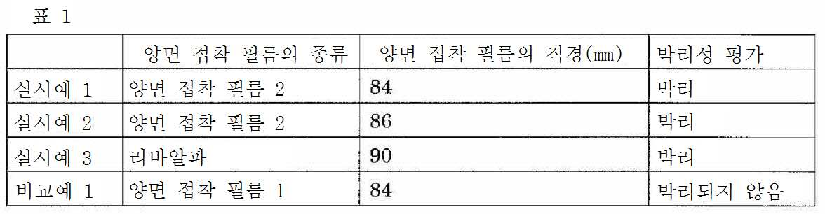
도 4는 실시예에 있어서의 박리성 평가 방법을 설명하는 도면이다.


Claims (5)
- 지지 기판(a) 상에 접착 필름(b)을 개재해서 전자 부재(c)가 접착된 적층체로부터, 상기 전자 부재(c)를 박리하는 방법으로서,
상기 접착 필름(b)은, 상기 지지 기판(a)측에 자기 박리형 접착층을 구비함과 더불어, 상기 전자 부재(c)측의 면의 적어도 일부가 노출된 영역을 구비하고,
상기 영역에 에너지를 부여하여, 해당 영역의 상기 지지 기판(a)과 상기 자기 박리형 접착층의 접착력을 저하시키는 공정과,
에너지를 더 부여하여, 접착력이 저하된, 상기 영역의 상기 지지 기판(a)과 상기 자기 박리형 접착층의 계면을 기점으로 해서, 상기 지지 기판(a)과 상기 자기 박리형 접착층의 접착력을 저하시켜 상기 지지 기판(a)을 제거하는 공정과,
상기 전자 부재(c)로부터 상기 접착 필름(b)을 제거하여, 상기 전자 부재(c)를 박리하는 공정
을 포함하는, 전자 부재의 박리 방법. - 제 1 항에 있어서,
상기 에너지가 열, 광, 진동, 응력 및 초음파로부터 선택되는 어느 하나인, 전자 부재의 박리 방법. - 제 1 항 또는 제 2 항에 있어서,
상기 접착 필름(b)이 노출되어 있는 상기 영역은, 상기 전자 부재(c)의 외연 전체를 따라 존재하는, 전자 부재의 박리 방법. - 제 1 항 내지 제 3 항 중 어느 한 항에 있어서,
상기 전자 부재(c)는 실리콘 웨이퍼, 세라믹 콘덴서 또는 반도체 패키지인, 전자 부재의 박리 방법. - 지지 기판(a) 상에 접착 필름(b)을 개재해서 전자 부재(c)가 접착된 적층체로서,
상기 접착 필름(b)은, 상기 지지 기판(a)측에 자기 박리형 접착층을 구비함과 더불어, 상기 전자 부재(c)측의 면의 적어도 일부가 노출된 영역을 구비하는, 적층체.
Applications Claiming Priority (3)
| Application Number | Priority Date | Filing Date | Title |
|---|---|---|---|
| JP2013115704 | 2013-05-31 | ||
| JPJP-P-2013-115704 | 2013-05-31 | ||
| PCT/JP2014/063578 WO2014192631A1 (ja) | 2013-05-31 | 2014-05-22 | 電子部材の剥離方法および積層体 |
Publications (2)
| Publication Number | Publication Date |
|---|---|
| KR20150140801A true KR20150140801A (ko) | 2015-12-16 |
| KR101772787B1 KR101772787B1 (ko) | 2017-08-29 |
Family
ID=51988664
Family Applications (1)
| Application Number | Title | Priority Date | Filing Date |
|---|---|---|---|
| KR1020157032145A Expired - Fee Related KR101772787B1 (ko) | 2013-05-31 | 2014-05-22 | 전자 부재의 박리 방법 및 적층체 |
Country Status (8)
| Country | Link |
|---|---|
| US (1) | US20160141197A1 (ko) |
| EP (1) | EP3007211A4 (ko) |
| JP (1) | JP6118404B2 (ko) |
| KR (1) | KR101772787B1 (ko) |
| CN (1) | CN105264645B (ko) |
| SG (1) | SG11201509300PA (ko) |
| TW (1) | TWI626152B (ko) |
| WO (1) | WO2014192631A1 (ko) |
Families Citing this family (10)
| Publication number | Priority date | Publication date | Assignee | Title |
|---|---|---|---|---|
| TWI681232B (zh) * | 2017-09-26 | 2020-01-01 | 達邁科技股份有限公司 | 用於軟性顯示器之透明聚醯亞胺複合膜及其製造方法 |
| TWI633816B (zh) * | 2017-11-08 | 2018-08-21 | Unimicron Technology Corp. | 電路板的製造方法 |
| CN108615700A (zh) * | 2018-04-26 | 2018-10-02 | 上海空间电源研究所 | 一种薄型太阳电池刚性-柔性衬底有机键合转移工艺方法 |
| TWI714890B (zh) * | 2018-09-28 | 2021-01-01 | 景碩科技股份有限公司 | 起膜機構 |
| TWI728915B (zh) * | 2018-09-28 | 2021-05-21 | 景碩科技股份有限公司 | 起膜機構 |
| JP7719604B2 (ja) * | 2018-10-05 | 2025-08-06 | 三井化学Ictマテリア株式会社 | 粘着性フィルムおよび電子装置の製造方法 |
| CN113135436B (zh) * | 2020-01-20 | 2023-02-17 | 上海广矩自动化设备有限公司 | 一种粘性片剥离方法 |
| US20220306177A1 (en) * | 2021-03-24 | 2022-09-29 | PulseForge Inc. | Method for attaching and detaching substrates during integrated circuit manufacturing |
| JP7794642B2 (ja) * | 2022-01-11 | 2026-01-06 | トヨタ自動車株式会社 | 電極の製造方法 |
| CN114639635B (zh) * | 2022-03-17 | 2023-03-21 | 电子科技大学 | 一种单晶薄膜的剥离方法、单晶薄膜以及电子元器件 |
Citations (9)
| Publication number | Priority date | Publication date | Assignee | Title |
|---|---|---|---|---|
| JPH04238037A (ja) | 1991-01-21 | 1992-08-26 | Furukawa Electric Co Ltd:The | クリーム半田の印刷装置 |
| JPH056497A (ja) | 1991-06-27 | 1993-01-14 | Kokusai Electric Co Ltd | 自動車用警報装置 |
| JPH0543851A (ja) | 1991-08-14 | 1993-02-23 | Nitto Denko Corp | 剥離性感圧接着剤及びその粘着部材 |
| JPH11166164A (ja) | 1997-12-01 | 1999-06-22 | Nitto Denko Corp | 加熱剥離型粘着シート |
| JP2001200234A (ja) | 2000-01-21 | 2001-07-24 | Asahi Kasei Corp | 半導体ウエハー固定用の粘着剤ならびに加工方法 |
| JP2003151940A (ja) | 2001-11-15 | 2003-05-23 | Sekisui Chem Co Ltd | バックグラインドテープ及び半導体ウエハの研磨方法 |
| JP2003173993A (ja) | 2001-12-04 | 2003-06-20 | Sekisui Chem Co Ltd | バックグラインドテープ及び半導体ウエハの研磨方法 |
| JP2003173989A (ja) | 2001-12-04 | 2003-06-20 | Sekisui Chem Co Ltd | Icチップの製造方法 |
| US8114766B1 (en) | 2005-09-19 | 2012-02-14 | Renesas Electronics Corporation | Method for manufacturing semiconductor device |
Family Cites Families (18)
| Publication number | Priority date | Publication date | Assignee | Title |
|---|---|---|---|---|
| JPH0831778A (ja) * | 1994-07-15 | 1996-02-02 | Toshiba Corp | 半導体装置の製造方法 |
| JP3438369B2 (ja) * | 1995-01-17 | 2003-08-18 | ソニー株式会社 | 部材の製造方法 |
| JP5006497B2 (ja) | 2001-08-03 | 2012-08-22 | 積水化学工業株式会社 | 両面粘着テープ及び両面粘着テープの剥離方法 |
| JP4238037B2 (ja) | 2001-11-15 | 2009-03-11 | 積水化学工業株式会社 | 接着性物質、接着性物質の剥離方法及び粘着テープ |
| DE60325669D1 (de) * | 2002-05-17 | 2009-02-26 | Semiconductor Energy Lab | Verfahren zum Transferieren eines Objekts und Verfahren zur Herstellung eines Halbleiterbauelements |
| JP2003338474A (ja) * | 2002-05-21 | 2003-11-28 | Lintec Corp | 脆質部材の加工方法 |
| JP4060641B2 (ja) * | 2002-05-22 | 2008-03-12 | 株式会社ディスコ | テープ剥離方法 |
| JP4565804B2 (ja) * | 2002-06-03 | 2010-10-20 | スリーエム イノベイティブ プロパティズ カンパニー | 被研削基材を含む積層体、その製造方法並びに積層体を用いた極薄基材の製造方法及びそのための装置 |
| JP2004253482A (ja) * | 2003-02-18 | 2004-09-09 | Dainippon Printing Co Ltd | 機能性素子の製造方法 |
| JP4592270B2 (ja) * | 2003-10-06 | 2010-12-01 | 日東電工株式会社 | 半導体ウエハの支持材からの剥離方法およびこれを用いた装置 |
| JP4208856B2 (ja) * | 2004-04-28 | 2009-01-14 | キヤノン株式会社 | 液体吐出ヘッドの製造方法 |
| CN101019206A (zh) * | 2004-08-02 | 2007-08-15 | 积水化学工业株式会社 | Ic芯片的制造方法 |
| JP4704828B2 (ja) * | 2004-09-29 | 2011-06-22 | 積水化学工業株式会社 | ウエハ貼着用粘着シート及びダイ接着用接着剤層付きicチップの製造方法 |
| JP2011040419A (ja) | 2008-05-22 | 2011-02-24 | Fuji Electric Systems Co Ltd | 半導体装置の製造方法及びそのための装置 |
| JP5252283B2 (ja) * | 2008-10-15 | 2013-07-31 | 富士電機株式会社 | 半導体装置の製造方法及びそのための装置 |
| US8950459B2 (en) * | 2009-04-16 | 2015-02-10 | Suss Microtec Lithography Gmbh | Debonding temporarily bonded semiconductor wafers |
| JP2010283098A (ja) * | 2009-06-04 | 2010-12-16 | Lintec Corp | 板状部材の支持部材 |
| US9847243B2 (en) * | 2009-08-27 | 2017-12-19 | Corning Incorporated | Debonding a glass substrate from carrier using ultrasonic wave |
-
2014
- 2014-05-22 WO PCT/JP2014/063578 patent/WO2014192631A1/ja not_active Ceased
- 2014-05-22 EP EP14803829.2A patent/EP3007211A4/en not_active Withdrawn
- 2014-05-22 JP JP2015519820A patent/JP6118404B2/ja active Active
- 2014-05-22 KR KR1020157032145A patent/KR101772787B1/ko not_active Expired - Fee Related
- 2014-05-22 SG SG11201509300PA patent/SG11201509300PA/en unknown
- 2014-05-22 CN CN201480028844.5A patent/CN105264645B/zh not_active Expired - Fee Related
- 2014-05-22 US US14/891,865 patent/US20160141197A1/en not_active Abandoned
- 2014-05-28 TW TW103118655A patent/TWI626152B/zh not_active IP Right Cessation
Patent Citations (9)
| Publication number | Priority date | Publication date | Assignee | Title |
|---|---|---|---|---|
| JPH04238037A (ja) | 1991-01-21 | 1992-08-26 | Furukawa Electric Co Ltd:The | クリーム半田の印刷装置 |
| JPH056497A (ja) | 1991-06-27 | 1993-01-14 | Kokusai Electric Co Ltd | 自動車用警報装置 |
| JPH0543851A (ja) | 1991-08-14 | 1993-02-23 | Nitto Denko Corp | 剥離性感圧接着剤及びその粘着部材 |
| JPH11166164A (ja) | 1997-12-01 | 1999-06-22 | Nitto Denko Corp | 加熱剥離型粘着シート |
| JP2001200234A (ja) | 2000-01-21 | 2001-07-24 | Asahi Kasei Corp | 半導体ウエハー固定用の粘着剤ならびに加工方法 |
| JP2003151940A (ja) | 2001-11-15 | 2003-05-23 | Sekisui Chem Co Ltd | バックグラインドテープ及び半導体ウエハの研磨方法 |
| JP2003173993A (ja) | 2001-12-04 | 2003-06-20 | Sekisui Chem Co Ltd | バックグラインドテープ及び半導体ウエハの研磨方法 |
| JP2003173989A (ja) | 2001-12-04 | 2003-06-20 | Sekisui Chem Co Ltd | Icチップの製造方法 |
| US8114766B1 (en) | 2005-09-19 | 2012-02-14 | Renesas Electronics Corporation | Method for manufacturing semiconductor device |
Also Published As
| Publication number | Publication date |
|---|---|
| JP6118404B2 (ja) | 2017-04-19 |
| WO2014192631A1 (ja) | 2014-12-04 |
| TW201444679A (zh) | 2014-12-01 |
| TWI626152B (zh) | 2018-06-11 |
| US20160141197A1 (en) | 2016-05-19 |
| EP3007211A4 (en) | 2016-12-14 |
| SG11201509300PA (en) | 2015-12-30 |
| JPWO2014192631A1 (ja) | 2017-02-23 |
| CN105264645B (zh) | 2018-05-01 |
| EP3007211A1 (en) | 2016-04-13 |
| KR101772787B1 (ko) | 2017-08-29 |
| CN105264645A (zh) | 2016-01-20 |
Similar Documents
| Publication | Publication Date | Title |
|---|---|---|
| KR101772787B1 (ko) | 전자 부재의 박리 방법 및 적층체 | |
| KR101785883B1 (ko) | 접착 필름 및 반도체 장치의 제조 방법 | |
| TWI806973B (zh) | 背面研磨用黏著膠布 | |
| JP4703833B2 (ja) | エネルギー線硬化型熱剥離性粘着シート、及びこれを用いた切断片の製造方法 | |
| JP2003045938A (ja) | 加熱剥離型粘着シートからのチップ切断片の加熱剥離方法、電子部品および回路基板 | |
| WO2008053840A1 (en) | Thermally strippable double faced adhesive sheet and method of working work piece | |
| JP5997477B2 (ja) | 表面保護用シート | |
| JP5318435B2 (ja) | 半導体ウエハの裏面研削用粘着シート及びこの裏面研削用粘着シートを用いる半導体ウエハの裏面研削方法 | |
| WO2004065510A1 (ja) | 粘着シート、半導体ウエハの表面保護方法およびワークの加工方法 | |
| CN102077135A (zh) | 电子纸的制造方法以及电子纸形成工序用双面粘合带 | |
| JP2005116610A (ja) | 半導体ウエハの加工方法および半導体ウエハ加工用粘着シート | |
| JP5997478B2 (ja) | 表面保護用シート | |
| CN107735855A (zh) | 电子部件保护膜、电子部件保护构件、电子部件的制造方法以及封装体的制造方法 | |
| JP2013222846A (ja) | 基板のダイシング方法 | |
| TW202334358A (zh) | 黏著帶 | |
| JP5565174B2 (ja) | 耐熱仮着用粘着テープ | |
| JP5351458B2 (ja) | ウェハ加工用接着シートおよび半導体装置の製造方法 | |
| JP2008066336A (ja) | ウエハ加工用シート | |
| JP2014086478A (ja) | イメージセンサの製造方法およびそれに用いる積層型耐熱性保護テープ | |
| TWI830764B (zh) | 端子保護用膠帶以及附電磁波屏蔽膜之半導體裝置的製造方法 | |
| JP2009032799A (ja) | ウェハ加工用テープ | |
| TWI681232B (zh) | 用於軟性顯示器之透明聚醯亞胺複合膜及其製造方法 | |
| WO2013089983A1 (en) | Dicing tape for rough surface die attach film | |
| JP2005097470A (ja) | 粘着フィルムと被着体の剥離帯電性の調整方法 |
Legal Events
| Date | Code | Title | Description |
|---|---|---|---|
| A201 | Request for examination | ||
| AMND | Amendment | ||
| P11-X000 | Amendment of application requested |
St.27 status event code: A-2-2-P10-P11-nap-X000 |
|
| P13-X000 | Application amended |
St.27 status event code: A-2-2-P10-P13-nap-X000 |
|
| PA0105 | International application |
St.27 status event code: A-0-1-A10-A15-nap-PA0105 |
|
| PA0201 | Request for examination |
St.27 status event code: A-1-2-D10-D11-exm-PA0201 |
|
| PG1501 | Laying open of application |
St.27 status event code: A-1-1-Q10-Q12-nap-PG1501 |
|
| D13-X000 | Search requested |
St.27 status event code: A-1-2-D10-D13-srh-X000 |
|
| D14-X000 | Search report completed |
St.27 status event code: A-1-2-D10-D14-srh-X000 |
|
| E902 | Notification of reason for refusal | ||
| PE0902 | Notice of grounds for rejection |
St.27 status event code: A-1-2-D10-D21-exm-PE0902 |
|
| T11-X000 | Administrative time limit extension requested |
St.27 status event code: U-3-3-T10-T11-oth-X000 |
|
| AMND | Amendment | ||
| E13-X000 | Pre-grant limitation requested |
St.27 status event code: A-2-3-E10-E13-lim-X000 |
|
| P11-X000 | Amendment of application requested |
St.27 status event code: A-2-2-P10-P11-nap-X000 |
|
| P13-X000 | Application amended |
St.27 status event code: A-2-2-P10-P13-nap-X000 |
|
| PN2301 | Change of applicant |
St.27 status event code: A-3-3-R10-R13-asn-PN2301 St.27 status event code: A-3-3-R10-R11-asn-PN2301 |
|
| E601 | Decision to refuse application | ||
| PE0601 | Decision on rejection of patent |
St.27 status event code: N-2-6-B10-B15-exm-PE0601 |
|
| AMND | Amendment | ||
| P11-X000 | Amendment of application requested |
St.27 status event code: A-2-2-P10-P11-nap-X000 |
|
| P13-X000 | Application amended |
St.27 status event code: A-2-2-P10-P13-nap-X000 |
|
| PX0901 | Re-examination |
St.27 status event code: A-2-3-E10-E12-rex-PX0901 |
|
| PX0701 | Decision of registration after re-examination |
St.27 status event code: A-3-4-F10-F13-rex-PX0701 |
|
| X701 | Decision to grant (after re-examination) | ||
| GRNT | Written decision to grant | ||
| PR0701 | Registration of establishment |
St.27 status event code: A-2-4-F10-F11-exm-PR0701 |
|
| PR1002 | Payment of registration fee |
St.27 status event code: A-2-2-U10-U12-oth-PR1002 Fee payment year number: 1 |
|
| PG1601 | Publication of registration |
St.27 status event code: A-4-4-Q10-Q13-nap-PG1601 |
|
| P22-X000 | Classification modified |
St.27 status event code: A-4-4-P10-P22-nap-X000 |
|
| PC1903 | Unpaid annual fee |
St.27 status event code: A-4-4-U10-U13-oth-PC1903 Not in force date: 20200824 Payment event data comment text: Termination Category : DEFAULT_OF_REGISTRATION_FEE |
|
| PC1903 | Unpaid annual fee |
St.27 status event code: N-4-6-H10-H13-oth-PC1903 Ip right cessation event data comment text: Termination Category : DEFAULT_OF_REGISTRATION_FEE Not in force date: 20200824 |
|
| PN2301 | Change of applicant |
St.27 status event code: A-5-5-R10-R13-asn-PN2301 St.27 status event code: A-5-5-R10-R11-asn-PN2301 |
|
| R11 | Change to the name of applicant or owner or transfer of ownership requested |
Free format text: ST27 STATUS EVENT CODE: A-5-5-R10-R11-ASN-PN2301 (AS PROVIDED BY THE NATIONAL OFFICE) |
|
| R13 | Change to the name of applicant or owner recorded |
Free format text: ST27 STATUS EVENT CODE: A-5-5-R10-R13-ASN-PN2301 (AS PROVIDED BY THE NATIONAL OFFICE) |
|
| P22-X000 | Classification modified |
St.27 status event code: A-4-4-P10-P22-nap-X000 |
|
| P22-X000 | Classification modified |
St.27 status event code: A-4-4-P10-P22-nap-X000 |