KR20150143868A - 반도체 기판 및 그 제조 방법, 태양 전지 소자, 그리고 태양 전지 - Google Patents
반도체 기판 및 그 제조 방법, 태양 전지 소자, 그리고 태양 전지 Download PDFInfo
- Publication number
- KR20150143868A KR20150143868A KR1020157034213A KR20157034213A KR20150143868A KR 20150143868 A KR20150143868 A KR 20150143868A KR 1020157034213 A KR1020157034213 A KR 1020157034213A KR 20157034213 A KR20157034213 A KR 20157034213A KR 20150143868 A KR20150143868 A KR 20150143868A
- Authority
- KR
- South Korea
- Prior art keywords
- diffusion layer
- impurity
- type
- atoms
- type impurity
- Prior art date
- Legal status (The legal status is an assumption and is not a legal conclusion. Google has not performed a legal analysis and makes no representation as to the accuracy of the status listed.)
- Ceased
Links
Images
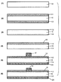
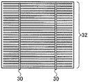
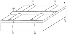
Classifications
-
- H01L31/0288—
-
- H—ELECTRICITY
- H10—SEMICONDUCTOR DEVICES; ELECTRIC SOLID-STATE DEVICES NOT OTHERWISE PROVIDED FOR
- H10F—INORGANIC SEMICONDUCTOR DEVICES SENSITIVE TO INFRARED RADIATION, LIGHT, ELECTROMAGNETIC RADIATION OF SHORTER WAVELENGTH OR CORPUSCULAR RADIATION
- H10F77/00—Constructional details of devices covered by this subclass
- H10F77/70—Surface textures, e.g. pyramid structures
- H10F77/703—Surface textures, e.g. pyramid structures of the semiconductor bodies, e.g. textured active layers
-
- H01L31/02021—
-
- H01L31/02363—
-
- H01L31/02366—
-
- H01L31/02725—
-
- H01L31/0392—
-
- H01L31/18—
-
- H—ELECTRICITY
- H10—SEMICONDUCTOR DEVICES; ELECTRIC SOLID-STATE DEVICES NOT OTHERWISE PROVIDED FOR
- H10D—INORGANIC ELECTRIC SEMICONDUCTOR DEVICES
- H10D62/00—Semiconductor bodies, or regions thereof, of devices having potential barriers
- H10D62/60—Impurity distributions or concentrations
-
- H—ELECTRICITY
- H10—SEMICONDUCTOR DEVICES; ELECTRIC SOLID-STATE DEVICES NOT OTHERWISE PROVIDED FOR
- H10F—INORGANIC SEMICONDUCTOR DEVICES SENSITIVE TO INFRARED RADIATION, LIGHT, ELECTROMAGNETIC RADIATION OF SHORTER WAVELENGTH OR CORPUSCULAR RADIATION
- H10F10/00—Individual photovoltaic cells, e.g. solar cells
- H10F10/10—Individual photovoltaic cells, e.g. solar cells having potential barriers
- H10F10/14—Photovoltaic cells having only PN homojunction potential barriers
-
- H—ELECTRICITY
- H10—SEMICONDUCTOR DEVICES; ELECTRIC SOLID-STATE DEVICES NOT OTHERWISE PROVIDED FOR
- H10F—INORGANIC SEMICONDUCTOR DEVICES SENSITIVE TO INFRARED RADIATION, LIGHT, ELECTROMAGNETIC RADIATION OF SHORTER WAVELENGTH OR CORPUSCULAR RADIATION
- H10F71/00—Manufacture or treatment of devices covered by this subclass
- H10F71/121—The active layers comprising only Group IV materials
-
- H—ELECTRICITY
- H10—SEMICONDUCTOR DEVICES; ELECTRIC SOLID-STATE DEVICES NOT OTHERWISE PROVIDED FOR
- H10F—INORGANIC SEMICONDUCTOR DEVICES SENSITIVE TO INFRARED RADIATION, LIGHT, ELECTROMAGNETIC RADIATION OF SHORTER WAVELENGTH OR CORPUSCULAR RADIATION
- H10F77/00—Constructional details of devices covered by this subclass
- H10F77/20—Electrodes
- H10F77/206—Electrodes for devices having potential barriers
- H10F77/211—Electrodes for devices having potential barriers for photovoltaic cells
-
- H—ELECTRICITY
- H10—SEMICONDUCTOR DEVICES; ELECTRIC SOLID-STATE DEVICES NOT OTHERWISE PROVIDED FOR
- H10P—GENERIC PROCESSES OR APPARATUS FOR THE MANUFACTURE OR TREATMENT OF DEVICES COVERED BY CLASS H10
- H10P32/00—Diffusion of dopants within, into or out of wafers, substrates or parts of devices
- H10P32/10—Diffusion of dopants within, into or out of semiconductor bodies or layers
- H10P32/14—Diffusion of dopants within, into or out of semiconductor bodies or layers within a single semiconductor body or layer in a solid phase; between different semiconductor bodies or layers, both in a solid phase
- H10P32/1408—Diffusion of dopants within, into or out of semiconductor bodies or layers within a single semiconductor body or layer in a solid phase; between different semiconductor bodies or layers, both in a solid phase from or through or into an external applied layer, e.g. photoresist or nitride layers
- H10P32/141—Diffusion of dopants within, into or out of semiconductor bodies or layers within a single semiconductor body or layer in a solid phase; between different semiconductor bodies or layers, both in a solid phase from or through or into an external applied layer, e.g. photoresist or nitride layers the applied layer comprising oxides only
-
- H—ELECTRICITY
- H10—SEMICONDUCTOR DEVICES; ELECTRIC SOLID-STATE DEVICES NOT OTHERWISE PROVIDED FOR
- H10P—GENERIC PROCESSES OR APPARATUS FOR THE MANUFACTURE OR TREATMENT OF DEVICES COVERED BY CLASS H10
- H10P32/00—Diffusion of dopants within, into or out of wafers, substrates or parts of devices
- H10P32/10—Diffusion of dopants within, into or out of semiconductor bodies or layers
- H10P32/17—Diffusion of dopants within, into or out of semiconductor bodies or layers characterised by the semiconductor material
- H10P32/171—Diffusion of dopants within, into or out of semiconductor bodies or layers characterised by the semiconductor material being group IV material
-
- Y—GENERAL TAGGING OF NEW TECHNOLOGICAL DEVELOPMENTS; GENERAL TAGGING OF CROSS-SECTIONAL TECHNOLOGIES SPANNING OVER SEVERAL SECTIONS OF THE IPC; TECHNICAL SUBJECTS COVERED BY FORMER USPC CROSS-REFERENCE ART COLLECTIONS [XRACs] AND DIGESTS
- Y02—TECHNOLOGIES OR APPLICATIONS FOR MITIGATION OR ADAPTATION AGAINST CLIMATE CHANGE
- Y02E—REDUCTION OF GREENHOUSE GAS [GHG] EMISSIONS, RELATED TO ENERGY GENERATION, TRANSMISSION OR DISTRIBUTION
- Y02E10/00—Energy generation through renewable energy sources
- Y02E10/50—Photovoltaic [PV] energy
-
- Y—GENERAL TAGGING OF NEW TECHNOLOGICAL DEVELOPMENTS; GENERAL TAGGING OF CROSS-SECTIONAL TECHNOLOGIES SPANNING OVER SEVERAL SECTIONS OF THE IPC; TECHNICAL SUBJECTS COVERED BY FORMER USPC CROSS-REFERENCE ART COLLECTIONS [XRACs] AND DIGESTS
- Y02—TECHNOLOGIES OR APPLICATIONS FOR MITIGATION OR ADAPTATION AGAINST CLIMATE CHANGE
- Y02E—REDUCTION OF GREENHOUSE GAS [GHG] EMISSIONS, RELATED TO ENERGY GENERATION, TRANSMISSION OR DISTRIBUTION
- Y02E10/00—Energy generation through renewable energy sources
- Y02E10/50—Photovoltaic [PV] energy
- Y02E10/547—Monocrystalline silicon PV cells
-
- Y—GENERAL TAGGING OF NEW TECHNOLOGICAL DEVELOPMENTS; GENERAL TAGGING OF CROSS-SECTIONAL TECHNOLOGIES SPANNING OVER SEVERAL SECTIONS OF THE IPC; TECHNICAL SUBJECTS COVERED BY FORMER USPC CROSS-REFERENCE ART COLLECTIONS [XRACs] AND DIGESTS
- Y02—TECHNOLOGIES OR APPLICATIONS FOR MITIGATION OR ADAPTATION AGAINST CLIMATE CHANGE
- Y02P—CLIMATE CHANGE MITIGATION TECHNOLOGIES IN THE PRODUCTION OR PROCESSING OF GOODS
- Y02P70/00—Climate change mitigation technologies in the production process for final industrial or consumer products
- Y02P70/50—Manufacturing or production processes characterised by the final manufactured product
Landscapes
- Photovoltaic Devices (AREA)
- Engineering & Computer Science (AREA)
- Life Sciences & Earth Sciences (AREA)
- Sustainable Development (AREA)
- Sustainable Energy (AREA)
- Manufacturing & Machinery (AREA)
Applications Claiming Priority (7)
| Application Number | Priority Date | Filing Date | Title |
|---|---|---|---|
| JPJP-P-2011-162645 | 2011-07-25 | ||
| JP2011162647 | 2011-07-25 | ||
| JP2011162645 | 2011-07-25 | ||
| JPJP-P-2011-162647 | 2011-07-25 | ||
| JP2011162646 | 2011-07-25 | ||
| JPJP-P-2011-162646 | 2011-07-25 | ||
| PCT/JP2012/068720 WO2013015284A1 (fr) | 2011-07-25 | 2012-07-24 | Substrat à semi-conducteur, son procédé de fabrication, élément de photopile et photopile |
Related Parent Applications (1)
| Application Number | Title | Priority Date | Filing Date |
|---|---|---|---|
| KR1020147001889A Division KR101719885B1 (ko) | 2011-07-25 | 2012-07-24 | 반도체 기판 및 그 제조 방법, 태양 전지 소자, 그리고 태양 전지 |
Publications (1)
| Publication Number | Publication Date |
|---|---|
| KR20150143868A true KR20150143868A (ko) | 2015-12-23 |
Family
ID=47596222
Family Applications (2)
| Application Number | Title | Priority Date | Filing Date |
|---|---|---|---|
| KR1020157034213A Ceased KR20150143868A (ko) | 2011-07-25 | 2012-07-24 | 반도체 기판 및 그 제조 방법, 태양 전지 소자, 그리고 태양 전지 |
| KR1020147001889A Ceased KR101719885B1 (ko) | 2011-07-25 | 2012-07-24 | 반도체 기판 및 그 제조 방법, 태양 전지 소자, 그리고 태양 전지 |
Family Applications After (1)
| Application Number | Title | Priority Date | Filing Date |
|---|---|---|---|
| KR1020147001889A Ceased KR101719885B1 (ko) | 2011-07-25 | 2012-07-24 | 반도체 기판 및 그 제조 방법, 태양 전지 소자, 그리고 태양 전지 |
Country Status (7)
| Country | Link |
|---|---|
| US (3) | US20130025670A1 (fr) |
| EP (1) | EP2728624A4 (fr) |
| JP (3) | JPWO2013015284A1 (fr) |
| KR (2) | KR20150143868A (fr) |
| CN (2) | CN103718309B (fr) |
| TW (1) | TWI502753B (fr) |
| WO (1) | WO2013015284A1 (fr) |
Families Citing this family (12)
| Publication number | Priority date | Publication date | Assignee | Title |
|---|---|---|---|---|
| JP5176159B1 (ja) * | 2011-07-19 | 2013-04-03 | 日立化成株式会社 | n型拡散層形成組成物、n型拡散層の製造方法、及び太陽電池素子の製造方法 |
| JP6232993B2 (ja) * | 2013-12-12 | 2017-11-22 | 日立化成株式会社 | 半導体基板の製造方法、半導体基板、太陽電池素子の製造方法及び太陽電池素子 |
| TW201528531A (zh) * | 2013-12-20 | 2015-07-16 | 日立化成股份有限公司 | 半導體基板的製造方法、半導體基板、太陽電池元件的製造方法及太陽電池元件 |
| EP3264446B1 (fr) * | 2015-02-25 | 2019-11-27 | Toray Industries, Inc. | Composition de diffusion d'impuretés de type p, procédé de fabrication d'élément semi-conducteur à l'aide de cette composition, et procédé de fabrication d'une cellule solaire |
| JP6366840B2 (ja) * | 2015-07-02 | 2018-08-01 | 三菱電機株式会社 | 太陽電池セルおよび太陽電池セルの製造方法 |
| US10593948B2 (en) * | 2015-09-30 | 2020-03-17 | Zeon Corporation | Binder composition for non-aqueous secondary battery electrode, slurry composition for non-aqueous secondary battery electrode, electrode for non-aqueous secondary battery, and non-aqueous secondary battery |
| WO2017099020A1 (fr) * | 2015-12-07 | 2017-06-15 | 東レ株式会社 | Procédé de production d'élément semi-conducteur et procédé de production de cellule solaire |
| JP6614348B2 (ja) * | 2016-07-04 | 2019-12-04 | 三菱電機株式会社 | 太陽電池セルの評価用基板および太陽電池セルの評価方法 |
| CN106835286B (zh) * | 2016-12-28 | 2019-01-22 | 东方环晟光伏(江苏)有限公司 | 一种太阳能电池的双面扩散工艺 |
| JP6933006B2 (ja) * | 2017-06-09 | 2021-09-08 | 横浜ゴム株式会社 | 空気入りタイヤ |
| KR102870227B1 (ko) * | 2018-01-30 | 2025-10-14 | 브라이트 뷰 테크놀로지즈 코포레이션 | 램버시안 분포를 갖는 광을 배트윙 분포로 변환하기 위한 마이크로구조체 |
| US20240258447A1 (en) * | 2023-01-31 | 2024-08-01 | Lawrence Livermore National Security, Llc | DIFFUSED B-Ga2O3 PHOTOCONDUCTIVE DEVICES |
Family Cites Families (33)
| Publication number | Priority date | Publication date | Assignee | Title |
|---|---|---|---|---|
| NL207969A (fr) * | 1955-06-28 | |||
| JPS5936418B2 (ja) * | 1975-10-25 | 1984-09-04 | 株式会社東芝 | シリコン基板に対する不純物拡散方法 |
| US4019924A (en) * | 1975-11-14 | 1977-04-26 | Mobil Tyco Solar Energy Corporation | Solar cell mounting and interconnecting assembly |
| US4124410A (en) * | 1977-11-21 | 1978-11-07 | Union Carbide Corporation | Silicon solar cells with low-cost substrates |
| US4239554A (en) * | 1978-07-17 | 1980-12-16 | Shunpei Yamazaki | Semiconductor photoelectric conversion device |
| US4235651A (en) * | 1979-03-19 | 1980-11-25 | Hughes Aircraft Company | Fabrication of GaAs-GaAlAs solar cells |
| JPS57132372A (en) * | 1981-02-09 | 1982-08-16 | Univ Tohoku | Manufacture of p-n junction type thin silicon band |
| US5096505A (en) * | 1990-05-21 | 1992-03-17 | The Boeing Company | Panel for solar concentrators and tandem cell units |
| JP3578539B2 (ja) * | 1996-02-08 | 2004-10-20 | 三菱電機株式会社 | 太陽電池の製造方法および太陽電池構造 |
| US6339013B1 (en) * | 1997-05-13 | 2002-01-15 | The Board Of Trustees Of The University Of Arkansas | Method of doping silicon, metal doped silicon, method of making solar cells, and solar cells |
| DE19910816A1 (de) | 1999-03-11 | 2000-10-05 | Merck Patent Gmbh | Dotierpasten zur Erzeugung von p,p+ und n,n+ Bereichen in Halbleitern |
| IT249780Y1 (it) * | 2000-03-17 | 2003-05-28 | Artemide Spa | Dispositivo di illuminazione polivalente |
| JP2002075894A (ja) | 2000-09-01 | 2002-03-15 | Sanken Electric Co Ltd | 液状不純物源材料及びこれを使用した半導体装置の製造方法 |
| US6524880B2 (en) * | 2001-04-23 | 2003-02-25 | Samsung Sdi Co., Ltd. | Solar cell and method for fabricating the same |
| JP4726354B2 (ja) * | 2001-08-22 | 2011-07-20 | 東洋アルミニウム株式会社 | ペースト組成物およびそれを用いた太陽電池 |
| JP4481869B2 (ja) * | 2005-04-26 | 2010-06-16 | 信越半導体株式会社 | 太陽電池の製造方法及び太陽電池並びに半導体装置の製造方法 |
| JP4541243B2 (ja) * | 2005-07-22 | 2010-09-08 | 日本合成化学工業株式会社 | ホウ素拡散用塗布液 |
| US8575474B2 (en) * | 2006-03-20 | 2013-11-05 | Heracus Precious Metals North America Conshohocken LLC | Solar cell contacts containing aluminum and at least one of boron, titanium, nickel, tin, silver, gallium, zinc, indium and copper |
| US8076570B2 (en) * | 2006-03-20 | 2011-12-13 | Ferro Corporation | Aluminum-boron solar cell contacts |
| JP4998923B2 (ja) * | 2006-08-10 | 2012-08-15 | 国立大学法人 筑波大学 | シリコンベースの高効率太陽電池およびその製造方法 |
| FR2906405B1 (fr) * | 2006-09-22 | 2008-12-19 | Commissariat Energie Atomique | Procede de realisation de regions dopees dans un substrat et de cellule photovoltaique |
| US7825329B2 (en) * | 2007-01-03 | 2010-11-02 | Solopower, Inc. | Thin film solar cell manufacturing and integration |
| US20090004486A1 (en) * | 2007-06-27 | 2009-01-01 | Sarah Arsenault | Corrosion inhibiting additive |
| US20090194157A1 (en) * | 2008-02-01 | 2009-08-06 | Guardian Industries Corp. | Front electrode having etched surface for use in photovoltaic device and method of making same |
| JP5522900B2 (ja) * | 2008-02-22 | 2014-06-18 | 東京応化工業株式会社 | 電極形成用導電性組成物及び太陽電池の形成方法 |
| JP2011035024A (ja) * | 2009-07-30 | 2011-02-17 | Toyo Aluminium Kk | ペースト組成物およびそれを用いた太陽電池素子 |
| JP5815215B2 (ja) * | 2009-08-27 | 2015-11-17 | 東京応化工業株式会社 | 拡散剤組成物、および不純物拡散層の形成方法 |
| JP5555469B2 (ja) * | 2009-10-05 | 2014-07-23 | 東京応化工業株式会社 | 拡散剤組成物、および不純物拡散層の形成方法 |
| JP4868079B1 (ja) * | 2010-01-25 | 2012-02-01 | 日立化成工業株式会社 | n型拡散層形成組成物、n型拡散層の製造方法、及び太陽電池セルの製造方法 |
| US20110195540A1 (en) * | 2010-02-05 | 2011-08-11 | Hitachi Chemical Company, Ltd. | Composition for forming p-type diffusion layer, method for forming p-type diffusion layer, and method for producing photovoltaic cell |
| JP2011162646A (ja) | 2010-02-09 | 2011-08-25 | Asahi Kasei Chemicals Corp | 硬化性組成物 |
| JP2011162647A (ja) | 2010-02-09 | 2011-08-25 | Toray Ind Inc | 多分岐ポリエステルおよびその組成物 |
| JP2011162645A (ja) | 2010-02-09 | 2011-08-25 | Asahi Kasei Chemicals Corp | 多孔質構造体 |
-
2012
- 2012-07-24 WO PCT/JP2012/068720 patent/WO2013015284A1/fr not_active Ceased
- 2012-07-24 JP JP2013525728A patent/JPWO2013015284A1/ja active Pending
- 2012-07-24 CN CN201280036330.5A patent/CN103718309B/zh not_active Expired - Fee Related
- 2012-07-24 CN CN201510959055.XA patent/CN105448677A/zh active Pending
- 2012-07-24 KR KR1020157034213A patent/KR20150143868A/ko not_active Ceased
- 2012-07-24 KR KR1020147001889A patent/KR101719885B1/ko not_active Ceased
- 2012-07-24 EP EP12817928.0A patent/EP2728624A4/fr not_active Withdrawn
- 2012-07-24 US US13/557,188 patent/US20130025670A1/en not_active Abandoned
- 2012-07-25 TW TW101126793A patent/TWI502753B/zh active
-
2013
- 2013-11-24 US US14/088,418 patent/US20140076396A1/en not_active Abandoned
-
2015
- 2015-09-02 JP JP2015172574A patent/JP2016015511A/ja active Pending
- 2015-10-09 US US14/879,733 patent/US20160035915A1/en not_active Abandoned
-
2016
- 2016-12-08 JP JP2016238300A patent/JP2017085126A/ja active Pending
Also Published As
| Publication number | Publication date |
|---|---|
| EP2728624A4 (fr) | 2015-05-27 |
| KR20140041797A (ko) | 2014-04-04 |
| US20160035915A1 (en) | 2016-02-04 |
| CN103718309A (zh) | 2014-04-09 |
| CN103718309B (zh) | 2018-05-18 |
| US20140076396A1 (en) | 2014-03-20 |
| JP2017085126A (ja) | 2017-05-18 |
| KR101719885B1 (ko) | 2017-03-24 |
| WO2013015284A1 (fr) | 2013-01-31 |
| TWI502753B (zh) | 2015-10-01 |
| EP2728624A1 (fr) | 2014-05-07 |
| US20130025670A1 (en) | 2013-01-31 |
| TW201310662A (zh) | 2013-03-01 |
| JP2016015511A (ja) | 2016-01-28 |
| JPWO2013015284A1 (ja) | 2015-02-23 |
| CN105448677A (zh) | 2016-03-30 |
Similar Documents
| Publication | Publication Date | Title |
|---|---|---|
| KR101719885B1 (ko) | 반도체 기판 및 그 제조 방법, 태양 전지 소자, 그리고 태양 전지 | |
| KR20170086001A (ko) | n 형 확산층 형성 조성물, n 형 확산층의 제조 방법, 및 태양 전지 셀의 제조 방법 | |
| KR101835897B1 (ko) | n 형 확산층 형성 조성물, n 형 확산층의 제조 방법, 및 태양 전지 소자의 제조 방법 | |
| US20140060385A1 (en) | Composition for forming n-type diffusion layer, method for forming n-type diffusion layer, and method for producing photovoltaic cell | |
| KR20170045744A (ko) | p 형 확산층 형성 조성물, p 형 확산층의 제조 방법, 및 태양 전지 셀의 제조 방법 | |
| KR101541657B1 (ko) | 태양 전지 기판, 태양 전지 기판의 제조 방법, 태양 전지 소자 및 태양 전지 | |
| JP5958485B2 (ja) | n型拡散層形成組成物、n型拡散層の製造方法、及び太陽電池素子の製造方法 | |
| KR101541660B1 (ko) | n 형 확산층 형성 조성물, n 형 확산층의 제조 방법, 및 태양 전지 소자의 제조 방법 | |
| WO2011162394A1 (fr) | COMPOSITION DE FORMATION DE COUCHE DE DIFFUSION D'IMPURETÉS, COMPOSITION DE FORMATION DE COUCHE DE DIFFUSION DE TYPE n, PROCÉDÉ DE FABRICATION DE COUCHE DE DIFFUSION DE TYPE n, COMPOSITION DE FORMATION DE COUCHE DE DIFFUSION DE TYPE p, PROCÉDÉ DE FABRICATION DE COUCHE DE DIFFUSION DE TYPE p, ET PROCÉDÉ DE FABRICATION D'ÉLÉMENTS DE CELLULE SOLAIRE | |
| JP5935254B2 (ja) | 不純物拡散層形成組成物、不純物拡散層の製造方法、太陽電池素子の製造方法および太陽電池の製造方法 | |
| JP5541358B2 (ja) | n型拡散層形成組成物、n型拡散層の製造方法、及び太陽電池素子の製造方法 | |
| WO2011132782A1 (fr) | COMPOSITION FORMANT UNE COUCHE DE DIFFUSION DE TYPE p, PROCÉDÉ DE PRODUCTION D'UNE COUCHE DE DIFFUSION DE TYPE p ET PROCÉDÉ DE PRODUCTION D'UN ÉLÉMENT DE CELLULE SOLAIRE | |
| JP2013026477A (ja) | n型拡散層形成組成物、n型拡散層の製造方法、及び太陽電池素子の製造方法 |
Legal Events
| Date | Code | Title | Description |
|---|---|---|---|
| A107 | Divisional application of patent | ||
| PA0104 | Divisional application for international application |
Comment text: Divisional Application for International Patent Patent event code: PA01041R01D Patent event date: 20151130 Application number text: 1020147001889 Filing date: 20140123 |
|
| PG1501 | Laying open of application | ||
| A201 | Request for examination | ||
| PA0201 | Request for examination |
Patent event code: PA02012R01D Patent event date: 20170724 Comment text: Request for Examination of Application |
|
| E902 | Notification of reason for refusal | ||
| PE0902 | Notice of grounds for rejection |
Comment text: Notification of reason for refusal Patent event date: 20170821 Patent event code: PE09021S01D |
|
| AMND | Amendment | ||
| E601 | Decision to refuse application | ||
| PE0601 | Decision on rejection of patent |
Patent event date: 20180627 Comment text: Decision to Refuse Application Patent event code: PE06012S01D Patent event date: 20170821 Comment text: Notification of reason for refusal Patent event code: PE06011S01I |
|
| X091 | Application refused [patent] | ||
| AMND | Amendment | ||
| PX0901 | Re-examination |
Patent event code: PX09011S01I Patent event date: 20180627 Comment text: Decision to Refuse Application Patent event code: PX09012R01I Patent event date: 20180221 Comment text: Amendment to Specification, etc. |
|
| PX0601 | Decision of rejection after re-examination |
Comment text: Decision to Refuse Application Patent event code: PX06014S01D Patent event date: 20181101 Comment text: Amendment to Specification, etc. Patent event code: PX06012R01I Patent event date: 20180927 Comment text: Decision to Refuse Application Patent event code: PX06011S01I Patent event date: 20180627 Comment text: Amendment to Specification, etc. Patent event code: PX06012R01I Patent event date: 20180221 Comment text: Notification of reason for refusal Patent event code: PX06013S01I Patent event date: 20170821 |
|
| J201 | Request for trial against refusal decision | ||
| PJ0201 | Trial against decision of rejection |
Patent event date: 20190130 Comment text: Request for Trial against Decision on Refusal Patent event code: PJ02012R01D Patent event date: 20181101 Comment text: Decision to Refuse Application Patent event code: PJ02011S01I Patent event date: 20180627 Comment text: Decision to Refuse Application Patent event code: PJ02011S01I Appeal kind category: Appeal against decision to decline refusal Appeal identifier: 2019101000336 Request date: 20190130 |
|
| J301 | Trial decision |
Free format text: TRIAL NUMBER: 2019101000336; TRIAL DECISION FOR APPEAL AGAINST DECISION TO DECLINE REFUSAL REQUESTED 20190130 Effective date: 20200204 |
|
| PJ1301 | Trial decision |
Patent event code: PJ13011S01D Patent event date: 20200204 Comment text: Trial Decision on Objection to Decision on Refusal Appeal kind category: Appeal against decision to decline refusal Request date: 20190130 Decision date: 20200204 Appeal identifier: 2019101000336 |