KR20160010404A - 통합 센서를 갖는 전계 발광 디바이스 및 그 디바이스의 방출을 제어하는 방법 - Google Patents
통합 센서를 갖는 전계 발광 디바이스 및 그 디바이스의 방출을 제어하는 방법 Download PDFInfo
- Publication number
- KR20160010404A KR20160010404A KR1020157026371A KR20157026371A KR20160010404A KR 20160010404 A KR20160010404 A KR 20160010404A KR 1020157026371 A KR1020157026371 A KR 1020157026371A KR 20157026371 A KR20157026371 A KR 20157026371A KR 20160010404 A KR20160010404 A KR 20160010404A
- Authority
- KR
- South Korea
- Prior art keywords
- nanowires
- primary
- voltage
- subset
- photocurrent
- Prior art date
- Legal status (The legal status is an assumption and is not a legal conclusion. Google has not performed a legal analysis and makes no representation as to the accuracy of the status listed.)
- Granted
Links
Images




Classifications
-
- H01L27/15—
-
- H—ELECTRICITY
- H05—ELECTRIC TECHNIQUES NOT OTHERWISE PROVIDED FOR
- H05B—ELECTRIC HEATING; ELECTRIC LIGHT SOURCES NOT OTHERWISE PROVIDED FOR; CIRCUIT ARRANGEMENTS FOR ELECTRIC LIGHT SOURCES, IN GENERAL
- H05B45/00—Circuit arrangements for operating light-emitting diodes [LED]
- H05B45/20—Controlling the colour of the light
-
- H01L21/02603—
-
- H01L27/156—
-
- H01L29/0669—
-
- H01L29/413—
-
- H01L31/153—
-
- H01L33/08—
-
- H01L33/16—
-
- H01L33/24—
-
- H—ELECTRICITY
- H10—SEMICONDUCTOR DEVICES; ELECTRIC SOLID-STATE DEVICES NOT OTHERWISE PROVIDED FOR
- H10F—INORGANIC SEMICONDUCTOR DEVICES SENSITIVE TO INFRARED RADIATION, LIGHT, ELECTROMAGNETIC RADIATION OF SHORTER WAVELENGTH OR CORPUSCULAR RADIATION
- H10F55/00—Radiation-sensitive semiconductor devices covered by groups H10F10/00, H10F19/00 or H10F30/00 being structurally associated with electric light sources and electrically or optically coupled thereto
- H10F55/10—Radiation-sensitive semiconductor devices covered by groups H10F10/00, H10F19/00 or H10F30/00 being structurally associated with electric light sources and electrically or optically coupled thereto wherein the radiation-sensitive semiconductor devices control the electric light source, e.g. image converters, image amplifiers or image storage devices
- H10F55/15—Radiation-sensitive semiconductor devices covered by groups H10F10/00, H10F19/00 or H10F30/00 being structurally associated with electric light sources and electrically or optically coupled thereto wherein the radiation-sensitive semiconductor devices control the electric light source, e.g. image converters, image amplifiers or image storage devices wherein the radiation-sensitive devices and the electric light source are all semiconductor devices
- H10F55/155—Radiation-sensitive semiconductor devices covered by groups H10F10/00, H10F19/00 or H10F30/00 being structurally associated with electric light sources and electrically or optically coupled thereto wherein the radiation-sensitive semiconductor devices control the electric light source, e.g. image converters, image amplifiers or image storage devices wherein the radiation-sensitive devices and the electric light source are all semiconductor devices formed in, or on, a common substrate
-
- H—ELECTRICITY
- H10—SEMICONDUCTOR DEVICES; ELECTRIC SOLID-STATE DEVICES NOT OTHERWISE PROVIDED FOR
- H10H—INORGANIC LIGHT-EMITTING SEMICONDUCTOR DEVICES HAVING POTENTIAL BARRIERS
- H10H20/00—Individual inorganic light-emitting semiconductor devices having potential barriers, e.g. light-emitting diodes [LED]
- H10H20/80—Constructional details
- H10H20/81—Bodies
- H10H20/811—Bodies having quantum effect structures or superlattices, e.g. tunnel junctions
- H10H20/812—Bodies having quantum effect structures or superlattices, e.g. tunnel junctions within the light-emitting regions, e.g. having quantum confinement structures
-
- H—ELECTRICITY
- H10—SEMICONDUCTOR DEVICES; ELECTRIC SOLID-STATE DEVICES NOT OTHERWISE PROVIDED FOR
- H10H—INORGANIC LIGHT-EMITTING SEMICONDUCTOR DEVICES HAVING POTENTIAL BARRIERS
- H10H20/00—Individual inorganic light-emitting semiconductor devices having potential barriers, e.g. light-emitting diodes [LED]
- H10H20/80—Constructional details
- H10H20/81—Bodies
- H10H20/813—Bodies having a plurality of light-emitting regions, e.g. multi-junction LEDs or light-emitting devices having photoluminescent regions within the bodies
-
- H—ELECTRICITY
- H10—SEMICONDUCTOR DEVICES; ELECTRIC SOLID-STATE DEVICES NOT OTHERWISE PROVIDED FOR
- H10H—INORGANIC LIGHT-EMITTING SEMICONDUCTOR DEVICES HAVING POTENTIAL BARRIERS
- H10H20/00—Individual inorganic light-emitting semiconductor devices having potential barriers, e.g. light-emitting diodes [LED]
- H10H20/80—Constructional details
- H10H20/81—Bodies
- H10H20/817—Bodies characterised by the crystal structures or orientations, e.g. polycrystalline, amorphous or porous
-
- H—ELECTRICITY
- H10—SEMICONDUCTOR DEVICES; ELECTRIC SOLID-STATE DEVICES NOT OTHERWISE PROVIDED FOR
- H10H—INORGANIC LIGHT-EMITTING SEMICONDUCTOR DEVICES HAVING POTENTIAL BARRIERS
- H10H20/00—Individual inorganic light-emitting semiconductor devices having potential barriers, e.g. light-emitting diodes [LED]
- H10H20/80—Constructional details
- H10H20/81—Bodies
- H10H20/819—Bodies characterised by their shape, e.g. curved or truncated substrates
- H10H20/821—Bodies characterised by their shape, e.g. curved or truncated substrates of the light-emitting regions, e.g. non-planar junctions
-
- H—ELECTRICITY
- H10—SEMICONDUCTOR DEVICES; ELECTRIC SOLID-STATE DEVICES NOT OTHERWISE PROVIDED FOR
- H10H—INORGANIC LIGHT-EMITTING SEMICONDUCTOR DEVICES HAVING POTENTIAL BARRIERS
- H10H20/00—Individual inorganic light-emitting semiconductor devices having potential barriers, e.g. light-emitting diodes [LED]
- H10H20/80—Constructional details
- H10H20/81—Bodies
- H10H20/822—Materials of the light-emitting regions
- H10H20/824—Materials of the light-emitting regions comprising only Group III-V materials, e.g. GaP
- H10H20/825—Materials of the light-emitting regions comprising only Group III-V materials, e.g. GaP containing nitrogen, e.g. GaN
-
- H—ELECTRICITY
- H10—SEMICONDUCTOR DEVICES; ELECTRIC SOLID-STATE DEVICES NOT OTHERWISE PROVIDED FOR
- H10H—INORGANIC LIGHT-EMITTING SEMICONDUCTOR DEVICES HAVING POTENTIAL BARRIERS
- H10H29/00—Integrated devices, or assemblies of multiple devices, comprising at least one light-emitting semiconductor element covered by group H10H20/00
- H10H29/10—Integrated devices comprising at least one light-emitting semiconductor component covered by group H10H20/00
-
- H—ELECTRICITY
- H10—SEMICONDUCTOR DEVICES; ELECTRIC SOLID-STATE DEVICES NOT OTHERWISE PROVIDED FOR
- H10H—INORGANIC LIGHT-EMITTING SEMICONDUCTOR DEVICES HAVING POTENTIAL BARRIERS
- H10H29/00—Integrated devices, or assemblies of multiple devices, comprising at least one light-emitting semiconductor element covered by group H10H20/00
- H10H29/10—Integrated devices comprising at least one light-emitting semiconductor component covered by group H10H20/00
- H10H29/14—Integrated devices comprising at least one light-emitting semiconductor component covered by group H10H20/00 comprising multiple light-emitting semiconductor components
- H10H29/142—Two-dimensional arrangements, e.g. asymmetric LED layout
Landscapes
- Electroluminescent Light Sources (AREA)
- Luminescent Compositions (AREA)
- Chemical & Material Sciences (AREA)
- Engineering & Computer Science (AREA)
- Nanotechnology (AREA)
- Materials Engineering (AREA)
- Led Devices (AREA)
Abstract
- 제 1 전기 컨택들에 접속된 나노와이어들을 포함하고 소위 순방향 전압 또는 전류 소스로부터의 소위 순방향 제 1 전압의 작용으로 광을 방출할 수 있는 일차의 소위 방출 나노와이어들 (NTie) 의 제 1 시리즈;
- 상기 일차 나노 와이어들에 인접하고, 제 2 전기 컨택들에 접속되며, 전압 또는 전류 소스로부터의 제 2 의 소위 역방향 전압의 제어하에, 주변 광 및/또는 상기 일차 나노와이어들의 일부에 의해 방출된 광의 부분의 작용으로 광전류를 생성할 수 있는 이차의 소위 검출 나노와이어들 (NTid) 의 제 2 시리즈; 및
- 상기 광전류에 따라 상기 소위 순방향 전압을 제어하는 수단을 포함하는 것을 특징으로 한다.
본 발명의 다른 주제는 본 발명에 따른 전계 발광 디바이스의 휘도를 제어하는 방법이다.
Description
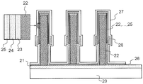
- 도 1 은 종래 기술에 따른 방사 구조를 갖는 나노와이어들을 사용하는 LED 구성을 도시한다.
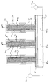
- 도 2 는 본 발명의 디바이스에서 이차 나노와이어들이 일차 나노와이어들에 인접하여 일차 나노와이어들에 의해 방출되는 광자들을 캡처하는 현상을 도시한다.
- 도 3 은 본 발명의 제 1 변형 디바이스를 도시한다.
- 도 4a (단면도) 및 도 4b (평면도) 는 본 발명에 따른 제 1 예시적인 디바이스를 도시한다.
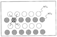
- 도 5 는 센서 부분의 광전류를 증폭하는 것을 가능하게 하는, 일차 나노와이어들과 이차 나노와이어들의 제 1 의 예시적인 분포를 도시한다.
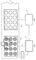
- 도 6 은 본 발명의 제 2 변형 디바이스를 도시한다.
- 도 7 은 휘도 맵핑을 생성하는 것을 가능하게 하는, 본 발명의 디바이스의 나노와이어들 전체에서 이차 나노와이어들의 제 2 의 예시적인 분포를 도시한다.
Claims (15)
- 기판의 표면 상에 나노와이어 세트를 포함하는 구조를 포함하는 전계 발광 디바이스로서,
- 제 1 전기 컨택들에 접속된 나노와이어들을 포함하고, 소위 순방향 전압 또는 전류 소스로부터의 소위 순방향 제 1 전압의 작용으로 광을 방출할 수 있는 일차의 소위 방출 나노와이어들 (NTie) 의 제 1 시리즈;
- 상기 일차 나노와이어들에 인접하고, 제 2 전기 컨택들에 접속되며, 전압 또는 전류 소스로부터의 제 2 의 소위 역방향 전압의 제어하에, 주변 광 및/또는 상기 일차 나노와이어들의 일부에 의해 방출된 광의 부분의 작용으로 광전류를 생성할 수 있는 이차의 소위 검출 나노와이어들 (NTid) 의 제 2 시리즈; 및
- 상기 광전류에 따라 상기 소위 순방향 전압을 제어하는 수단을 포함하는 것을 특징으로 하는 전계 발광 디바이스. - 제 1 항에 있어서,
상기 전계 발광 디바이스는 상기 광전류를 순방향 전압 또는 전류 소스에 주입하여 상기 순방향 전압을 조절하는 수단을 포함하며,
상기 수단은, 상기 구조 외부에 있고, 이차 나노와이어들에 의해 생성된 광전류 (Iph) 를 소정의 참조 전류 (Iref) 와 비교하고 상기 순방향 전압 또는 전류 소스의 전원 조절기 (11) 에 작용하여 일차 나노와이어들의 전압을 제어하는 전류 비교기를 포함하는 회로를 포함하는 것을 특징으로 하는 전계 발광 디바이스. - 제 1 항에 있어서,
- 상기 이차의 소위 검출 나노와이어들 (NTid) 의 제 2 시리즈는 주변 광의 존재 시, 0 의 전압 또는 역방향 전압의 제어하에 광전류 (Iph) 를 생성할 수 있는 검출 나노와이어들의 적어도 하나의 서브세트를 포함하며;
- 상기 전계 발광 디바이스는 상기 구조의 외부에 있고, 이차 나노와이어들에 의해 생성된 광전류를 임계 전류 (Iph.s) 와 비교하여, 상기 광전류 값 (Iph) 이 상기 임계 전류 값 (Iph.s) 미만일 경우, 스위치가 구비된 전원 (21) 을 통해 상기 전계 발광 디바이스를 활성화시키는 전류 비교기 (20) 를 포함하는 회로를 포함하는 것을 특징으로 하는 전계 발광 디바이스. - 제 1 항 내지 제 3 항 중 어느 한 항에 있어서,
상기 나노와이어들은 투명한 전도성 층으로 커버되고, 상기 일차 나노와이어들과 상기 이차 나노와이어들 사이에서 불연속하여 상기 제 2 전기 컨택들 중 하나로부터 상기 제 1 전기 컨택들 중 하나를 전기적으로 분리하는 것을 특징으로 하는 전계 발광 디바이스. - 제 1 항 내지 제 4 항 중 어느 한 항에 있어서,
상기 기판은 상기 나노와이어들을 포함하는 면과 대향하는 것으로 정의된 후면 상에, 상기 제 1 전기 컨택들 중 하나 및 상기 제 2 전기 컨택들 중 하나와 공통인 접촉 층을 포함하는 것을 특징으로 하는 전계 발광 디바이스. - 제 1 항 내지 제 5 항 중 어느 한 항에 있어서,
상기 전계 발광 디바이스는 상기 기판 위에 분포된 이차 나노와이어들의 서브세트들을 포함하는 것을 특징으로 하는 전계 발광 디바이스. - 제 1 항 내지 제 6 항 중 어느 한 항에 있어서,
상기 전계 발광 디바이스는 상이한 파장들 (λic) 에서 광자들을 방출할 수 있는 일차 나노와이어들의 복수의 서브세트들을 포함하며,
상기 전계 발광 디바이스는 상기 상이한 파장들 (λic) 에서의 방출들의 합으로부터 기인하는 합성 광을 방출하는 것을 특징으로 하는 전계 발광 디바이스. - 제 7 항에 있어서,
상기 전계 발광 디바이스는 이차 나노와이어들의 복수의 서브세트들을 포함하고, 상기 이차 나노와이어들의 각각의 서브세트는 파장 (λic) 에서 광자들을 방출하는 일차 나노와이어들의 서브세트에 인접하여 상기 파장 (λic) 에서 상기 광자들을 픽업할 수 있는 것을 특징으로 하는 전계 발광 디바이스. - 제 1 항 내지 제 8 항 중 어느 한 항에 있어서,
상기 나노와이어들은 Ⅲ-Ⅴ 재료들의 헤테로 접합에 기초한 구조들을 가지는 것을 특징으로 하는 전계 발광 디바이스. - 제 1 항 내지 제 9 항 중 어느 한 항에 기재된 전계 발광 디바이스를 제어하는 방법으로서,
- 전압 또는 전류 소스로부터의 제 2 의 소위 역방향 전압의 제어하에, 주변 광 및/또는 상기 일차 나노와이어들 중 일부에 의해 방출된 광의 부분의 작용으로 이차 나노와이어들의 적어도 하나의 서브세트로부터 적어도 하나의 광전류를 검출하는 단계;
- 상기 광전류에 따라 소위 순방향 전압의 작용으로 일차 나노와이어들의 적어도 하나의 서브세트를 제어하는 단계를 포함하는 것을 특징으로 하는 전계 발광 디바이스를 제어하는 방법. - 제 10 항에 있어서,
상기 전계 발광 디바이스를 제어하는 방법은, 상기 검출하는 단계 이전에, 일차의 소위 방출 나노와이어들 (NTie) 의 적어도 하나의 서브세트를 제어하는 단계를 포함하고, 상기 일차의 소위 방출 나노와이어들 (NTie) 의 방출은 상기 이차 나노와이어들에 의해 부분적으로 픽업되는 것을 특징으로 하는 전계 발광 디바이스를 제어하는 방법. - 제 11 항에 기재된 전계 발광 디바이스의 휘도를 제어하는 방법으로서,
- 일차 나노와이어들의 적어도 하나의 서브세트에 제 1 초기 전압을 인가하는 단계;
- 이차 나노와이어들의 적어도 하나의 서브세트에 역방향 전압을 인가하여 광전류를 검출하는 단계;
- 상기 일차 나노와이어들에 인가될 제어 전압의 결정시 상기 광전류를 통합하여 상기 전계 발광 디바이스의 휘도를 조절하는 단계를 포함하는 것을 특징으로 하는 전계 발광 디바이스의 휘도를 제어하는 방법. - 제 11 항에 기재된 전계 발광 디바이스의 표면 휘도의 분포를 제어하는 방법으로서,
- 일차 나노와이어들의 복수의 서브세트들에 제 1 초기 전압을 인가하는 것;
- 이차 나노와이어들의 복수의 서브세트들에 역방향 전압을 인가하는 것으로서, 상기 이차 나노와이어들의 각각의 서브세트는 파장에서 광자들을 방출하는 일차 나노와이어들의 서브세트에 인접하고, 상기 이차 나노와이어들은 상기 기판 전체에 걸쳐 분포되어 이차 나노와이어들의 서브세트마다 광전류를 검출하는, 상기 역방향 전압을 인가하는 것;
- 상기 이차 나노와이어들의 서브세트들과 각각 연관된 상기 일차 나노와이어들의 서브세트들에 인가될 제어 전압의 결정시 광전류들을 통합하여 상기 전계 발광 디바이스의 휘도의 표면 분포를 조절하는 것을 포함하는 것을 특징으로 하는 전계 발광 디바이스의 표면 휘도의 분포를 제어하는 방법. - 상이한 파장들 (λic) 에서 방출하는 나노와이어들의 복수의 서브세트들의 방출로부터 기인하는 합성 광을 방출하는, 제 7 항 또는 제 8 항에 기재된 전계 발광 디바이스의 색도를 제어하는 방법으로서,
- 일차 나노와이어들의 서브세트들에 제 1 초기 전압을 인가하는 것;
- 이차 나노와이어들의 복수의 서브세트들에 역방향 전압을 인가하는 것으로서, 상기 이차 나노와이어들의 각각의 서브세트는 파장 (λic) 에서 광자들을 방출하는 일차 나노와이어들의 서브세트에 인접하여 상기 파장 (λic) 에서 상기 광자들을 픽업할 수 있는, 상기 역방향 전압을 인가하는 것;
- 상기 이차 나노와이어들의 서브세트들과 각각 연관된 상기 일차 나노와이어들의 서브세트들에 인가될 제어 전압의 결정시 광전류들을 통합하여 상기 전계 발광 디바이스의 합성 색도를 조절하는 것을 포함하는 것을 특징으로 하는 전계 발광 디바이스의 색도를 제어하는 방법. - 제 10 항에 있어서,
상기 전계 발광 디바이스를 제어하는 방법은,
- 역방향 전압을 이차 나노와이어들의 적어도 하나의 서브세트에 인가하여 광전류 (Iph) 를 검출하는 단계;
- 상기 광전류를 전류 임계 값 (Iph.s) 과 비교하는 단계;
- 상기 광전류 값 (Iph) 이 상기 임계 전류 값 (Iph.s) 미만일 경우, 순방향 전압을 일차 나노와이어들에 인가하여 상기 전계 발광 디바이스를 활성화시키는 단계를 포함하는 것을 특징으로 하는 전계 발광 디바이스를 제어하는 방법.
Applications Claiming Priority (3)
| Application Number | Priority Date | Filing Date | Title |
|---|---|---|---|
| FR1352811A FR3004000B1 (fr) | 2013-03-28 | 2013-03-28 | Dispositif electroluminescent avec capteur integre et procede de controle de l'emission du dispositif |
| FR1352811 | 2013-03-28 | ||
| PCT/EP2014/055907 WO2014154657A1 (fr) | 2013-03-28 | 2014-03-25 | Dispositif electroluminescent avec capteur integre et procede de controle de l'emission du dispositif |
Publications (2)
| Publication Number | Publication Date |
|---|---|
| KR20160010404A true KR20160010404A (ko) | 2016-01-27 |
| KR102158894B1 KR102158894B1 (ko) | 2020-09-22 |
Family
ID=48699076
Family Applications (1)
| Application Number | Title | Priority Date | Filing Date |
|---|---|---|---|
| KR1020157026371A Active KR102158894B1 (ko) | 2013-03-28 | 2014-03-25 | 통합 센서를 갖는 전계 발광 디바이스 및 그 디바이스의 방출을 제어하는 방법 |
Country Status (6)
| Country | Link |
|---|---|
| US (1) | US9847446B2 (ko) |
| EP (1) | EP2979301B1 (ko) |
| JP (1) | JP6559116B2 (ko) |
| KR (1) | KR102158894B1 (ko) |
| FR (1) | FR3004000B1 (ko) |
| WO (1) | WO2014154657A1 (ko) |
Cited By (1)
| Publication number | Priority date | Publication date | Assignee | Title |
|---|---|---|---|---|
| WO2019121556A1 (de) * | 2017-12-20 | 2019-06-27 | Osram Opto Semiconductors Gmbh | Optoelektronisches halbleiterbauteil und verfahren zur herstellung von optoelektronischen halbleiterbauteilen |
Families Citing this family (4)
| Publication number | Priority date | Publication date | Assignee | Title |
|---|---|---|---|---|
| FR3058570B1 (fr) * | 2016-11-10 | 2019-05-24 | Valeo Vision | Source lumineuse a unites electroluminescentes avec fonction de detection |
| WO2019050939A1 (en) * | 2017-09-08 | 2019-03-14 | Lumileds Llc | OPTOELECTRONIC DEVICE AND ADAPTIVE LIGHTING SYSTEM USING THE SAME |
| US9974135B1 (en) | 2017-09-08 | 2018-05-15 | Lumileds Llc | Optoelectronic device and adaptive illumination system using the same |
| US11637219B2 (en) | 2019-04-12 | 2023-04-25 | Google Llc | Monolithic integration of different light emitting structures on a same substrate |
Citations (7)
| Publication number | Priority date | Publication date | Assignee | Title |
|---|---|---|---|---|
| JPH06224470A (ja) * | 1993-01-22 | 1994-08-12 | Ricoh Co Ltd | 光走査装置及び該装置による光走査方法 |
| WO2002048701A2 (en) * | 2000-12-11 | 2002-06-20 | President And Fellows Of Harvard College | Nanosensors |
| WO2002080280A1 (en) * | 2001-03-30 | 2002-10-10 | The Regents Of The University Of California | Methods of fabricating nanostructures and nanowires and devices fabricated therefrom |
| JP2004507104A (ja) * | 2000-08-22 | 2004-03-04 | プレジデント・アンド・フェローズ・オブ・ハーバード・カレッジ | ドープされた細長い半導体、そのような半導体の成長、そのような半導体を含んだデバイス、およびそのようなデバイスの製造 |
| KR20110039335A (ko) * | 2008-07-09 | 2011-04-15 | 큐나노 에이비 | 광전자 반도체 디바이스 |
| KR20110073493A (ko) * | 2008-09-04 | 2011-06-29 | 큐나노 에이비 | 나노구조 포토다이오드 |
| JP2013004661A (ja) * | 2011-06-15 | 2013-01-07 | Sharp Corp | 半導体素子、半導体素子の製造方法、発光ダイオード、発光ダイオードの製造方法、光電変換素子、太陽電池、照明装置、バックライトおよび表示装置 |
Family Cites Families (16)
| Publication number | Priority date | Publication date | Assignee | Title |
|---|---|---|---|---|
| JPS5394883A (en) * | 1977-01-31 | 1978-08-19 | Nec Corp | Light emission diode device |
| JPH09193461A (ja) * | 1996-01-24 | 1997-07-29 | Canon Inc | 画像形成方法及び装置 |
| KR100589621B1 (ko) * | 1998-03-12 | 2006-06-19 | 니치아 카가쿠 고교 가부시키가이샤 | 질화물 반도체 소자 |
| US6448550B1 (en) * | 2000-04-27 | 2002-09-10 | Agilent Technologies, Inc. | Method and apparatus for measuring spectral content of LED light source and control thereof |
| JP4160000B2 (ja) * | 2004-02-13 | 2008-10-01 | ドンゴク ユニバーシティ インダストリー アカデミック コーポレイション ファウンデイション | 発光ダイオードおよびその製造方法 |
| EP1727216B1 (en) * | 2005-05-24 | 2019-04-24 | LG Electronics, Inc. | Rod type light emitting diode and method for fabricating the same |
| US8227817B2 (en) * | 2006-12-22 | 2012-07-24 | Qunano Ab | Elevated LED |
| CN101657902B (zh) * | 2007-04-13 | 2012-01-11 | 夏普株式会社 | 光传感器和显示装置 |
| US8964020B2 (en) * | 2007-04-25 | 2015-02-24 | Stc.Unm | Solid-state microscope for selectively imaging a sample |
| JP5100719B2 (ja) * | 2009-08-07 | 2012-12-19 | シャープ株式会社 | 照明装置 |
| JP2011135058A (ja) * | 2009-11-30 | 2011-07-07 | Honda Motor Co Ltd | 太陽電池素子、カラーセンサ、ならびに発光素子及び受光素子の製造方法 |
| US8835903B2 (en) * | 2010-07-29 | 2014-09-16 | National Tsing Hua University | Light-emitting diode display and method of producing the same |
| FR2975532B1 (fr) * | 2011-05-18 | 2013-05-10 | Commissariat Energie Atomique | Connexion electrique en serie de nanofils emetteurs de lumiere |
| WO2012036124A1 (ja) * | 2010-09-17 | 2012-03-22 | シャープ株式会社 | Ledユニット、及び、ledディスプレイ |
| US8759777B2 (en) * | 2012-01-03 | 2014-06-24 | Capella Microsystems (Taiwan), Inc. | Infrared light detecting apparatus and detecting method thereof |
| US20150303332A1 (en) * | 2012-08-22 | 2015-10-22 | Northwestern University | Anodes, solar cells and methods of making same |
-
2013
- 2013-03-28 FR FR1352811A patent/FR3004000B1/fr active Active
-
2014
- 2014-03-25 US US14/778,017 patent/US9847446B2/en active Active
- 2014-03-25 JP JP2016504622A patent/JP6559116B2/ja active Active
- 2014-03-25 WO PCT/EP2014/055907 patent/WO2014154657A1/fr not_active Ceased
- 2014-03-25 KR KR1020157026371A patent/KR102158894B1/ko active Active
- 2014-03-25 EP EP14712658.5A patent/EP2979301B1/fr active Active
Patent Citations (7)
| Publication number | Priority date | Publication date | Assignee | Title |
|---|---|---|---|---|
| JPH06224470A (ja) * | 1993-01-22 | 1994-08-12 | Ricoh Co Ltd | 光走査装置及び該装置による光走査方法 |
| JP2004507104A (ja) * | 2000-08-22 | 2004-03-04 | プレジデント・アンド・フェローズ・オブ・ハーバード・カレッジ | ドープされた細長い半導体、そのような半導体の成長、そのような半導体を含んだデバイス、およびそのようなデバイスの製造 |
| WO2002048701A2 (en) * | 2000-12-11 | 2002-06-20 | President And Fellows Of Harvard College | Nanosensors |
| WO2002080280A1 (en) * | 2001-03-30 | 2002-10-10 | The Regents Of The University Of California | Methods of fabricating nanostructures and nanowires and devices fabricated therefrom |
| KR20110039335A (ko) * | 2008-07-09 | 2011-04-15 | 큐나노 에이비 | 광전자 반도체 디바이스 |
| KR20110073493A (ko) * | 2008-09-04 | 2011-06-29 | 큐나노 에이비 | 나노구조 포토다이오드 |
| JP2013004661A (ja) * | 2011-06-15 | 2013-01-07 | Sharp Corp | 半導体素子、半導体素子の製造方法、発光ダイオード、発光ダイオードの製造方法、光電変換素子、太陽電池、照明装置、バックライトおよび表示装置 |
Cited By (2)
| Publication number | Priority date | Publication date | Assignee | Title |
|---|---|---|---|---|
| WO2019121556A1 (de) * | 2017-12-20 | 2019-06-27 | Osram Opto Semiconductors Gmbh | Optoelektronisches halbleiterbauteil und verfahren zur herstellung von optoelektronischen halbleiterbauteilen |
| US11574952B2 (en) | 2017-12-20 | 2023-02-07 | Osram Oled Gmbh | Optoelectronic semiconductor component and method for producing optoelectronic semiconductor components |
Also Published As
| Publication number | Publication date |
|---|---|
| JP6559116B2 (ja) | 2019-08-14 |
| EP2979301B1 (fr) | 2017-05-31 |
| KR102158894B1 (ko) | 2020-09-22 |
| FR3004000B1 (fr) | 2016-07-15 |
| EP2979301A1 (fr) | 2016-02-03 |
| US9847446B2 (en) | 2017-12-19 |
| WO2014154657A1 (fr) | 2014-10-02 |
| JP2016518020A (ja) | 2016-06-20 |
| US20160284933A1 (en) | 2016-09-29 |
| FR3004000A1 (fr) | 2014-10-03 |
Similar Documents
| Publication | Publication Date | Title |
|---|---|---|
| KR102357920B1 (ko) | 전계 효과에 의해 도펀트들을 이온화하기 위한 p-n 접합 광전 소자 | |
| US8274206B2 (en) | Interdigitated multiple pixel arrays of light-emitting devices | |
| JP7209338B2 (ja) | 半導体素子 | |
| US20130221320A1 (en) | Led with embedded doped current blocking layer | |
| KR102158894B1 (ko) | 통합 센서를 갖는 전계 발광 디바이스 및 그 디바이스의 방출을 제어하는 방법 | |
| US20250142912A1 (en) | Semiconductor device | |
| JP5137563B2 (ja) | 横型構成電気光学デバイス | |
| US20150179880A1 (en) | Nitride semiconductor structure | |
| KR102852198B1 (ko) | 반도체 소자 | |
| EP4531119A1 (en) | Light emitting diode | |
| KR102657311B1 (ko) | 반도체 소자 | |
| KR102733181B1 (ko) | 반도체 소자 | |
| US20220320367A1 (en) | Optoelectronic device comprising light-emitting diodes | |
| KR100991742B1 (ko) | 광 검출기를 구비한 광소자 | |
| KR102643093B1 (ko) | 반도체 소자 및 조명장치 | |
| KR102752937B1 (ko) | 반도체 소자 | |
| US8344394B1 (en) | High-speed avalanche light emitting diode (ALED) and related apparatus and method | |
| KR102782063B1 (ko) | 반도체 소자 | |
| Guan et al. | InGaN/GaN nanowire flexible light emitting diodes and photodetectors | |
| CN110462835A (zh) | 半导体器件 | |
| KR101174331B1 (ko) | 에피 구조로 형성된 고효율 반도체 광소자 및 그 제조방법 | |
| CN119789561A (zh) | 一种氮化镓led与锗pd单片异质集成结构及其制备方法 | |
| KR20180071829A (ko) | 반도체 소자 | |
| Zhang et al. | ZnO nanowire-based Schottky-barrier-type UV light-emitting diodes | |
| KR20180071830A (ko) | 반도체 소자 |
Legal Events
| Date | Code | Title | Description |
|---|---|---|---|
| PA0105 | International application |
St.27 status event code: A-0-1-A10-A15-nap-PA0105 |
|
| P11-X000 | Amendment of application requested |
St.27 status event code: A-2-2-P10-P11-nap-X000 |
|
| P13-X000 | Application amended |
St.27 status event code: A-2-2-P10-P13-nap-X000 |
|
| PG1501 | Laying open of application |
St.27 status event code: A-1-1-Q10-Q12-nap-PG1501 |
|
| P22-X000 | Classification modified |
St.27 status event code: A-2-2-P10-P22-nap-X000 |
|
| A201 | Request for examination | ||
| PA0201 | Request for examination |
St.27 status event code: A-1-2-D10-D11-exm-PA0201 |
|
| R18-X000 | Changes to party contact information recorded |
St.27 status event code: A-3-3-R10-R18-oth-X000 |
|
| E902 | Notification of reason for refusal | ||
| PE0902 | Notice of grounds for rejection |
St.27 status event code: A-1-2-D10-D21-exm-PE0902 |
|
| T11-X000 | Administrative time limit extension requested |
St.27 status event code: U-3-3-T10-T11-oth-X000 |
|
| T11-X000 | Administrative time limit extension requested |
St.27 status event code: U-3-3-T10-T11-oth-X000 |
|
| P11-X000 | Amendment of application requested |
St.27 status event code: A-2-2-P10-P11-nap-X000 |
|
| P13-X000 | Application amended |
St.27 status event code: A-2-2-P10-P13-nap-X000 |
|
| E701 | Decision to grant or registration of patent right | ||
| PE0701 | Decision of registration |
St.27 status event code: A-1-2-D10-D22-exm-PE0701 |
|
| GRNT | Written decision to grant | ||
| PR0701 | Registration of establishment |
St.27 status event code: A-2-4-F10-F11-exm-PR0701 |
|
| PR1002 | Payment of registration fee |
St.27 status event code: A-2-2-U10-U12-oth-PR1002 Fee payment year number: 1 |
|
| PG1601 | Publication of registration |
St.27 status event code: A-4-4-Q10-Q13-nap-PG1601 |
|
| R18-X000 | Changes to party contact information recorded |
St.27 status event code: A-5-5-R10-R18-oth-X000 |
|
| PR1001 | Payment of annual fee |
St.27 status event code: A-4-4-U10-U11-oth-PR1001 Fee payment year number: 4 |
|
| PR1001 | Payment of annual fee |
St.27 status event code: A-4-4-U10-U11-oth-PR1001 Fee payment year number: 5 |
|
| P22-X000 | Classification modified |
St.27 status event code: A-4-4-P10-P22-nap-X000 |
|
| R18 | Changes to party contact information recorded |
Free format text: ST27 STATUS EVENT CODE: A-5-5-R10-R18-OTH-X000 (AS PROVIDED BY THE NATIONAL OFFICE) |
|
| R18-X000 | Changes to party contact information recorded |
St.27 status event code: A-5-5-R10-R18-oth-X000 |
|
| P22-X000 | Classification modified |
St.27 status event code: A-4-4-P10-P22-nap-X000 |