KR20160018366A - 다층막을 에칭하는 방법 - Google Patents
다층막을 에칭하는 방법 Download PDFInfo
- Publication number
- KR20160018366A KR20160018366A KR1020150106596A KR20150106596A KR20160018366A KR 20160018366 A KR20160018366 A KR 20160018366A KR 1020150106596 A KR1020150106596 A KR 1020150106596A KR 20150106596 A KR20150106596 A KR 20150106596A KR 20160018366 A KR20160018366 A KR 20160018366A
- Authority
- KR
- South Korea
- Prior art keywords
- gas
- film
- etching
- frequency power
- multilayer film
- Prior art date
- Legal status (The legal status is an assumption and is not a legal conclusion. Google has not performed a legal analysis and makes no representation as to the accuracy of the status listed.)
- Granted
Links
Images


Classifications
-
- H01L21/32137—
-
- H—ELECTRICITY
- H10—SEMICONDUCTOR DEVICES; ELECTRIC SOLID-STATE DEVICES NOT OTHERWISE PROVIDED FOR
- H10B—ELECTRONIC MEMORY DEVICES
- H10B69/00—Erasable-and-programmable ROM [EPROM] devices not provided for in groups H10B41/00 - H10B63/00, e.g. ultraviolet erasable-and-programmable ROM [UVEPROM] devices
-
- H—ELECTRICITY
- H01—ELECTRIC ELEMENTS
- H01J—ELECTRIC DISCHARGE TUBES OR DISCHARGE LAMPS
- H01J37/00—Discharge tubes with provision for introducing objects or material to be exposed to the discharge, e.g. for the purpose of examination or processing thereof
- H01J37/32—Gas-filled discharge tubes
- H01J37/32009—Arrangements for generation of plasma specially adapted for examination or treatment of objects, e.g. plasma sources
- H01J37/32082—Radio frequency generated discharge
- H01J37/32091—Radio frequency generated discharge the radio frequency energy being capacitively coupled to the plasma
-
- H—ELECTRICITY
- H01—ELECTRIC ELEMENTS
- H01J—ELECTRIC DISCHARGE TUBES OR DISCHARGE LAMPS
- H01J37/00—Discharge tubes with provision for introducing objects or material to be exposed to the discharge, e.g. for the purpose of examination or processing thereof
- H01J37/32—Gas-filled discharge tubes
- H01J37/32009—Arrangements for generation of plasma specially adapted for examination or treatment of objects, e.g. plasma sources
- H01J37/32082—Radio frequency generated discharge
- H01J37/32137—Radio frequency generated discharge controlling of the discharge by modulation of energy
- H01J37/32155—Frequency modulation
- H01J37/32165—Plural frequencies
-
- H01L21/3065—
-
- H01L21/31116—
-
- H01L21/31144—
-
- H01L27/11556—
-
- H01L27/11582—
-
- H—ELECTRICITY
- H10—SEMICONDUCTOR DEVICES; ELECTRIC SOLID-STATE DEVICES NOT OTHERWISE PROVIDED FOR
- H10P—GENERIC PROCESSES OR APPARATUS FOR THE MANUFACTURE OR TREATMENT OF DEVICES COVERED BY CLASS H10
- H10P50/00—Etching of wafers, substrates or parts of devices
- H10P50/20—Dry etching; Plasma etching; Reactive-ion etching
- H10P50/26—Dry etching; Plasma etching; Reactive-ion etching of conductive or resistive materials
- H10P50/264—Dry etching; Plasma etching; Reactive-ion etching of conductive or resistive materials by chemical means
- H10P50/266—Dry etching; Plasma etching; Reactive-ion etching of conductive or resistive materials by chemical means by vapour etching only
- H10P50/267—Dry etching; Plasma etching; Reactive-ion etching of conductive or resistive materials by chemical means by vapour etching only using plasmas
- H10P50/268—Dry etching; Plasma etching; Reactive-ion etching of conductive or resistive materials by chemical means by vapour etching only using plasmas of silicon-containing layers
-
- H—ELECTRICITY
- H10—SEMICONDUCTOR DEVICES; ELECTRIC SOLID-STATE DEVICES NOT OTHERWISE PROVIDED FOR
- H10P—GENERIC PROCESSES OR APPARATUS FOR THE MANUFACTURE OR TREATMENT OF DEVICES COVERED BY CLASS H10
- H10P50/00—Etching of wafers, substrates or parts of devices
- H10P50/20—Dry etching; Plasma etching; Reactive-ion etching
- H10P50/28—Dry etching; Plasma etching; Reactive-ion etching of insulating materials
- H10P50/282—Dry etching; Plasma etching; Reactive-ion etching of insulating materials of inorganic materials
- H10P50/283—Dry etching; Plasma etching; Reactive-ion etching of insulating materials of inorganic materials by chemical means
-
- H—ELECTRICITY
- H01—ELECTRIC ELEMENTS
- H01J—ELECTRIC DISCHARGE TUBES OR DISCHARGE LAMPS
- H01J2237/00—Discharge tubes exposing object to beam, e.g. for analysis treatment, etching, imaging
- H01J2237/32—Processing objects by plasma generation
- H01J2237/33—Processing objects by plasma generation characterised by the type of processing
- H01J2237/334—Etching
-
- H—ELECTRICITY
- H10—SEMICONDUCTOR DEVICES; ELECTRIC SOLID-STATE DEVICES NOT OTHERWISE PROVIDED FOR
- H10B—ELECTRONIC MEMORY DEVICES
- H10B41/00—Electrically erasable-and-programmable ROM [EEPROM] devices comprising floating gates
- H10B41/20—Electrically erasable-and-programmable ROM [EEPROM] devices comprising floating gates characterised by three-dimensional [3D] arrangements, e.g. with cells on different height levels
- H10B41/23—Electrically erasable-and-programmable ROM [EEPROM] devices comprising floating gates characterised by three-dimensional [3D] arrangements, e.g. with cells on different height levels with source and drain on different levels, e.g. with sloping channels
- H10B41/27—Electrically erasable-and-programmable ROM [EEPROM] devices comprising floating gates characterised by three-dimensional [3D] arrangements, e.g. with cells on different height levels with source and drain on different levels, e.g. with sloping channels the channels comprising vertical portions, e.g. U-shaped channels
-
- H—ELECTRICITY
- H10—SEMICONDUCTOR DEVICES; ELECTRIC SOLID-STATE DEVICES NOT OTHERWISE PROVIDED FOR
- H10B—ELECTRONIC MEMORY DEVICES
- H10B43/00—EEPROM devices comprising charge-trapping gate insulators
- H10B43/20—EEPROM devices comprising charge-trapping gate insulators characterised by three-dimensional [3D] arrangements, e.g. with cells on different height levels
- H10B43/23—EEPROM devices comprising charge-trapping gate insulators characterised by three-dimensional [3D] arrangements, e.g. with cells on different height levels with source and drain on different levels, e.g. with sloping channels
- H10B43/27—EEPROM devices comprising charge-trapping gate insulators characterised by three-dimensional [3D] arrangements, e.g. with cells on different height levels with source and drain on different levels, e.g. with sloping channels the channels comprising vertical portions, e.g. U-shaped channels
Landscapes
- Physics & Mathematics (AREA)
- Engineering & Computer Science (AREA)
- Plasma & Fusion (AREA)
- Chemical & Material Sciences (AREA)
- Analytical Chemistry (AREA)
- Drying Of Semiconductors (AREA)
- Semiconductor Memories (AREA)
- Plasma Technology (AREA)
- Non-Volatile Memory (AREA)
Abstract
Description
도 2는 공정(ST1)에 있어서 준비되는 웨이퍼의 일례를 나타내는 도이다.
도 3은 플라즈마 처리 장치의 일례를 개략적으로 나타내는 도이다.
도 4는 도 3에 나타내는 밸브군, 유량 제어기군 및 가스 소스군을 상세하게 나타내는 도이다.
도 5는 공정(ST2)에 있어서 에칭되고 있는 웨이퍼를 나타내는 도이다.
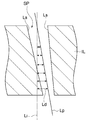
도 6은 실험예 및 비교 실험예에서 구한 경사각을 설명하기 위한 도이다.
도 7은 실험예 및 비교 실험예에서 구한 중심선의 이탈량을 설명하기 위한 도이다.
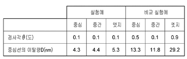
도 8은 실험예 및 비교 실험예에서 구한 경사각 및 중심선의 이탈량을 나타내는 표이다.
12 : 처리 용기
16 : 하부 전극
30 : 상부 전극
62 : 제 1 고주파 전원
64 : 제 2 고주파 전원
Cnt : 제어부
W : 웨이퍼
MSK : 마스크
IL : 다층막
IL1 : 유전체막
IL2 : 유전체막
SP : 스페이스
SW : 측벽면
PF : 보호막
Claims (8)
- 서로 상이한 유전율을 가지고, 또한 교호로 적층된 제 1 막 및 제 2 막을 포함하는 다층막을 에칭하는 방법으로서,
플라즈마 처리 장치의 처리 용기 내에, 상기 다층막 및 상기 다층막 상에 마련된 마스크를 가지는 피처리체를 준비하는 공정과,
상기 다층막을 에칭하는 공정으로, 수소 가스, 플루오르 하이드로 카본 가스, 불소 함유 가스, 탄화수소 가스, 삼염화 붕소 가스 및 질소 가스를 포함하는 처리 가스를 상기 처리 용기 내에서 여기시키는 상기 공정을 포함하는 방법. - 제 1 항에 있어서,
상기 플루오르 하이드로 카본 가스는 CH2F2 가스, CH3F 가스 또는 CHF3 가스인 방법. - 제 1 항 또는 제 2 항에 있어서,
상기 불소 함유 가스는 NF3 가스 또는 SF6 가스인 방법. - 제 1 항 또는 제 2 항에 있어서,
상기 탄화수소 가스는 CH4 가스인 방법. - 제 1 항 또는 제 2 항에 있어서,
상기 제 1 막은 산화 실리콘막이며, 상기 제 2 막은 질화 실리콘막인 방법. - 제 1 항 또는 제 2 항에 있어서,
상기 제 1 막은 산화 실리콘막이며, 상기 제 2 막은 폴리 실리콘막인 방법. - 제 1 항 또는 제 2 항에 있어서,
상기 제 1 막과 상기 제 2 막은 합계 24 층 이상 적층되어 있는 방법. - 제 1 항 또는 제 2 항에 있어서,
상기 마스크는 아몰퍼스 카본제인 방법.
Applications Claiming Priority (2)
| Application Number | Priority Date | Filing Date | Title |
|---|---|---|---|
| JP2014162809A JP6454492B2 (ja) | 2014-08-08 | 2014-08-08 | 多層膜をエッチングする方法 |
| JPJP-P-2014-162809 | 2014-08-08 |
Publications (2)
| Publication Number | Publication Date |
|---|---|
| KR20160018366A true KR20160018366A (ko) | 2016-02-17 |
| KR101835683B1 KR101835683B1 (ko) | 2018-03-07 |
Family
ID=55267936
Family Applications (1)
| Application Number | Title | Priority Date | Filing Date |
|---|---|---|---|
| KR1020150106596A Expired - Fee Related KR101835683B1 (ko) | 2014-08-08 | 2015-07-28 | 다층막을 에칭하는 방법 |
Country Status (5)
| Country | Link |
|---|---|
| US (1) | US9263239B1 (ko) |
| JP (1) | JP6454492B2 (ko) |
| KR (1) | KR101835683B1 (ko) |
| CN (1) | CN105374756B (ko) |
| SG (1) | SG10201506214XA (ko) |
Cited By (2)
| Publication number | Priority date | Publication date | Assignee | Title |
|---|---|---|---|---|
| KR20180000692A (ko) * | 2016-06-23 | 2018-01-03 | 도쿄엘렉트론가부시키가이샤 | 에칭 처리 방법 |
| KR20200047442A (ko) * | 2018-10-26 | 2020-05-07 | 주식회사 히타치하이테크 | 플라스마 처리 장치 및 플라스마 처리 방법 |
Families Citing this family (9)
| Publication number | Priority date | Publication date | Assignee | Title |
|---|---|---|---|---|
| JP6948181B2 (ja) * | 2017-08-01 | 2021-10-13 | 東京エレクトロン株式会社 | 多層膜をエッチングする方法 |
| JP7158252B2 (ja) * | 2018-02-15 | 2022-10-21 | 東京エレクトロン株式会社 | プラズマエッチング方法及びプラズマエッチング装置 |
| JP2020068221A (ja) * | 2018-10-22 | 2020-04-30 | 東京エレクトロン株式会社 | エッチング方法及びプラズマ処理装置 |
| JP7336365B2 (ja) * | 2019-11-19 | 2023-08-31 | 東京エレクトロン株式会社 | 膜をエッチングする方法及びプラズマ処理装置 |
| WO2021171458A1 (ja) | 2020-02-27 | 2021-09-02 | 株式会社日立ハイテク | プラズマ処理方法 |
| JP7565194B2 (ja) | 2020-11-12 | 2024-10-10 | 東京エレクトロン株式会社 | エッチング方法及びプラズマ処理装置 |
| JP7767024B2 (ja) * | 2021-05-07 | 2025-11-11 | 東京エレクトロン株式会社 | 基板処理方法および基板処理装置 |
| TW202407797A (zh) | 2022-03-01 | 2024-02-16 | 日商東京威力科創股份有限公司 | 電漿處理方法及電漿處理裝置 |
| JP7536941B2 (ja) | 2022-08-30 | 2024-08-20 | 東京エレクトロン株式会社 | プラズマ処理方法及びプラズマ処理装置 |
Citations (1)
| Publication number | Priority date | Publication date | Assignee | Title |
|---|---|---|---|---|
| WO2014010499A1 (ja) | 2012-07-10 | 2014-01-16 | 東京エレクトロン株式会社 | プラズマ処理方法及びプラズマ処理装置 |
Family Cites Families (13)
| Publication number | Priority date | Publication date | Assignee | Title |
|---|---|---|---|---|
| JPS5658972A (en) * | 1979-10-16 | 1981-05-22 | Chiyou Lsi Gijutsu Kenkyu Kumiai | Dry etching method |
| JPH0536645A (ja) * | 1991-07-25 | 1993-02-12 | Sony Corp | ドライエツチング方法 |
| TW383427B (en) * | 1998-04-03 | 2000-03-01 | United Microelectronics Corp | Method for etching tantalum oxide |
| JP4282391B2 (ja) * | 2003-07-09 | 2009-06-17 | Necエレクトロニクス株式会社 | 半導体装置の製造方法 |
| EP1780779A3 (en) * | 2005-10-28 | 2008-06-11 | Interuniversitair Microelektronica Centrum ( Imec) | A plasma for patterning advanced gate stacks |
| US20070221616A1 (en) * | 2006-03-24 | 2007-09-27 | Yi-Tyng Wu | Etching method |
| CN100428416C (zh) * | 2006-04-03 | 2008-10-22 | 中芯国际集成电路制造(上海)有限公司 | 半导体器件的制造方法 |
| US8598040B2 (en) * | 2011-09-06 | 2013-12-03 | Lam Research Corporation | ETCH process for 3D flash structures |
| JP6056136B2 (ja) * | 2011-09-07 | 2017-01-11 | セントラル硝子株式会社 | ドライエッチング方法 |
| CN102738074B (zh) * | 2012-07-05 | 2014-07-02 | 中微半导体设备(上海)有限公司 | 半导体结构的形成方法 |
| JP6096470B2 (ja) * | 2012-10-29 | 2017-03-15 | 東京エレクトロン株式会社 | プラズマ処理方法及びプラズマ処理装置 |
| WO2014069559A1 (ja) * | 2012-11-01 | 2014-05-08 | 東京エレクトロン株式会社 | プラズマ処理方法及びプラズマ処理装置 |
| JP6035117B2 (ja) * | 2012-11-09 | 2016-11-30 | 東京エレクトロン株式会社 | プラズマエッチング方法及びプラズマエッチング装置 |
-
2014
- 2014-08-08 JP JP2014162809A patent/JP6454492B2/ja not_active Expired - Fee Related
-
2015
- 2015-07-28 KR KR1020150106596A patent/KR101835683B1/ko not_active Expired - Fee Related
- 2015-08-04 US US14/817,393 patent/US9263239B1/en not_active Expired - Fee Related
- 2015-08-06 SG SG10201506214XA patent/SG10201506214XA/en unknown
- 2015-08-07 CN CN201510484931.8A patent/CN105374756B/zh not_active Expired - Fee Related
Patent Citations (1)
| Publication number | Priority date | Publication date | Assignee | Title |
|---|---|---|---|---|
| WO2014010499A1 (ja) | 2012-07-10 | 2014-01-16 | 東京エレクトロン株式会社 | プラズマ処理方法及びプラズマ処理装置 |
Cited By (2)
| Publication number | Priority date | Publication date | Assignee | Title |
|---|---|---|---|---|
| KR20180000692A (ko) * | 2016-06-23 | 2018-01-03 | 도쿄엘렉트론가부시키가이샤 | 에칭 처리 방법 |
| KR20200047442A (ko) * | 2018-10-26 | 2020-05-07 | 주식회사 히타치하이테크 | 플라스마 처리 장치 및 플라스마 처리 방법 |
Also Published As
| Publication number | Publication date |
|---|---|
| SG10201506214XA (en) | 2016-03-30 |
| CN105374756B (zh) | 2019-01-15 |
| CN105374756A (zh) | 2016-03-02 |
| US20160042918A1 (en) | 2016-02-11 |
| JP6454492B2 (ja) | 2019-01-16 |
| US9263239B1 (en) | 2016-02-16 |
| KR101835683B1 (ko) | 2018-03-07 |
| JP2016039309A (ja) | 2016-03-22 |
Similar Documents
| Publication | Publication Date | Title |
|---|---|---|
| KR101847866B1 (ko) | 다층막을 에칭하는 방법 | |
| KR101835683B1 (ko) | 다층막을 에칭하는 방법 | |
| KR102426264B1 (ko) | 에칭 방법 | |
| KR102320085B1 (ko) | 반도체 장치의 제조 방법 | |
| US9449838B2 (en) | Semiconductor device manufacturing method | |
| KR102038174B1 (ko) | 반도체 장치의 제조 방법 | |
| KR101937727B1 (ko) | 에칭 방법 | |
| US9418863B2 (en) | Method for etching etching target layer | |
| KR20150024277A (ko) | 반도체 장치의 제조 방법 | |
| KR20150021475A (ko) | 실리콘 산화막을 에칭하는 방법 | |
| KR20160134537A (ko) | 에칭 방법 |
Legal Events
| Date | Code | Title | Description |
|---|---|---|---|
| PA0109 | Patent application |
St.27 status event code: A-0-1-A10-A12-nap-PA0109 |
|
| PG1501 | Laying open of application |
St.27 status event code: A-1-1-Q10-Q12-nap-PG1501 |
|
| A201 | Request for examination | ||
| A302 | Request for accelerated examination | ||
| PA0201 | Request for examination |
St.27 status event code: A-1-2-D10-D11-exm-PA0201 |
|
| PA0302 | Request for accelerated examination |
St.27 status event code: A-1-2-D10-D17-exm-PA0302 St.27 status event code: A-1-2-D10-D16-exm-PA0302 |
|
| D13-X000 | Search requested |
St.27 status event code: A-1-2-D10-D13-srh-X000 |
|
| D14-X000 | Search report completed |
St.27 status event code: A-1-2-D10-D14-srh-X000 |
|
| E902 | Notification of reason for refusal | ||
| PE0902 | Notice of grounds for rejection |
St.27 status event code: A-1-2-D10-D21-exm-PE0902 |
|
| P11-X000 | Amendment of application requested |
St.27 status event code: A-2-2-P10-P11-nap-X000 |
|
| P13-X000 | Application amended |
St.27 status event code: A-2-2-P10-P13-nap-X000 |
|
| E701 | Decision to grant or registration of patent right | ||
| PE0701 | Decision of registration |
St.27 status event code: A-1-2-D10-D22-exm-PE0701 |
|
| PR0701 | Registration of establishment |
St.27 status event code: A-2-4-F10-F11-exm-PR0701 |
|
| PR1002 | Payment of registration fee |
St.27 status event code: A-2-2-U10-U11-oth-PR1002 Fee payment year number: 1 |
|
| PG1601 | Publication of registration |
St.27 status event code: A-4-4-Q10-Q13-nap-PG1601 |
|
| P22-X000 | Classification modified |
St.27 status event code: A-4-4-P10-P22-nap-X000 |
|
| PR1001 | Payment of annual fee |
St.27 status event code: A-4-4-U10-U11-oth-PR1001 Fee payment year number: 4 |
|
| PR1001 | Payment of annual fee |
St.27 status event code: A-4-4-U10-U11-oth-PR1001 Fee payment year number: 5 |
|
| P22-X000 | Classification modified |
St.27 status event code: A-4-4-P10-P22-nap-X000 |
|
| P22-X000 | Classification modified |
St.27 status event code: A-4-4-P10-P22-nap-X000 |
|
| PR1001 | Payment of annual fee |
St.27 status event code: A-4-4-U10-U11-oth-PR1001 Fee payment year number: 6 |
|
| PC1903 | Unpaid annual fee |
St.27 status event code: A-4-4-U10-U13-oth-PC1903 Not in force date: 20240301 Payment event data comment text: Termination Category : DEFAULT_OF_REGISTRATION_FEE |
|
| P22-X000 | Classification modified |
St.27 status event code: A-4-4-P10-P22-nap-X000 |
|
| PC1903 | Unpaid annual fee |
St.27 status event code: N-4-6-H10-H13-oth-PC1903 Ip right cessation event data comment text: Termination Category : DEFAULT_OF_REGISTRATION_FEE Not in force date: 20240301 |
|
| P22-X000 | Classification modified |
St.27 status event code: A-4-4-P10-P22-nap-X000 |