KR20160038325A - 색변환용 기판, 그 제조방법 및 이를 포함하는 디스플레이 장치 - Google Patents
색변환용 기판, 그 제조방법 및 이를 포함하는 디스플레이 장치 Download PDFInfo
- Publication number
- KR20160038325A KR20160038325A KR1020140130971A KR20140130971A KR20160038325A KR 20160038325 A KR20160038325 A KR 20160038325A KR 1020140130971 A KR1020140130971 A KR 1020140130971A KR 20140130971 A KR20140130971 A KR 20140130971A KR 20160038325 A KR20160038325 A KR 20160038325A
- Authority
- KR
- South Korea
- Prior art keywords
- quantum dot
- coating layer
- light guide
- thin plate
- guide plate
- Prior art date
- Legal status (The legal status is an assumption and is not a legal conclusion. Google has not performed a legal analysis and makes no representation as to the accuracy of the status listed.)
- Ceased
Links
Images
Classifications
-
- G—PHYSICS
- G02—OPTICS
- G02B—OPTICAL ELEMENTS, SYSTEMS OR APPARATUS
- G02B6/00—Light guides; Structural details of arrangements comprising light guides and other optical elements, e.g. couplings
- G02B6/02—Optical fibres with cladding with or without a coating
- G02B6/0229—Optical fibres with cladding with or without a coating characterised by nanostructures, i.e. structures of size less than 100 nm, e.g. quantum dots
-
- G—PHYSICS
- G02—OPTICS
- G02F—OPTICAL DEVICES OR ARRANGEMENTS FOR THE CONTROL OF LIGHT BY MODIFICATION OF THE OPTICAL PROPERTIES OF THE MEDIA OF THE ELEMENTS INVOLVED THEREIN; NON-LINEAR OPTICS; FREQUENCY-CHANGING OF LIGHT; OPTICAL LOGIC ELEMENTS; OPTICAL ANALOGUE/DIGITAL CONVERTERS
- G02F1/00—Devices or arrangements for the control of the intensity, colour, phase, polarisation or direction of light arriving from an independent light source, e.g. switching, gating or modulating; Non-linear optics
- G02F1/01—Devices or arrangements for the control of the intensity, colour, phase, polarisation or direction of light arriving from an independent light source, e.g. switching, gating or modulating; Non-linear optics for the control of the intensity, phase, polarisation or colour
- G02F1/13—Devices or arrangements for the control of the intensity, colour, phase, polarisation or direction of light arriving from an independent light source, e.g. switching, gating or modulating; Non-linear optics for the control of the intensity, phase, polarisation or colour based on liquid crystals, e.g. single liquid crystal display cells
- G02F1/133—Constructional arrangements; Operation of liquid crystal cells; Circuit arrangements
- G02F1/1333—Constructional arrangements; Manufacturing methods
- G02F1/1335—Structural association of cells with optical devices, e.g. polarisers or reflectors
- G02F1/1336—Illuminating devices
- G02F1/133615—Edge-illuminating devices, i.e. illuminating from the side
-
- F—MECHANICAL ENGINEERING; LIGHTING; HEATING; WEAPONS; BLASTING
- F21—LIGHTING
- F21V—FUNCTIONAL FEATURES OR DETAILS OF LIGHTING DEVICES OR SYSTEMS THEREOF; STRUCTURAL COMBINATIONS OF LIGHTING DEVICES WITH OTHER ARTICLES, NOT OTHERWISE PROVIDED FOR
- F21V9/00—Elements for modifying spectral properties, polarisation or intensity of the light emitted, e.g. filters
- F21V9/30—Elements containing photoluminescent material distinct from or spaced from the light source
- F21V9/32—Elements containing photoluminescent material distinct from or spaced from the light source characterised by the arrangement of the photoluminescent material
-
- F—MECHANICAL ENGINEERING; LIGHTING; HEATING; WEAPONS; BLASTING
- F21—LIGHTING
- F21V—FUNCTIONAL FEATURES OR DETAILS OF LIGHTING DEVICES OR SYSTEMS THEREOF; STRUCTURAL COMBINATIONS OF LIGHTING DEVICES WITH OTHER ARTICLES, NOT OTHERWISE PROVIDED FOR
- F21V9/00—Elements for modifying spectral properties, polarisation or intensity of the light emitted, e.g. filters
- F21V9/30—Elements containing photoluminescent material distinct from or spaced from the light source
-
- F—MECHANICAL ENGINEERING; LIGHTING; HEATING; WEAPONS; BLASTING
- F21—LIGHTING
- F21V—FUNCTIONAL FEATURES OR DETAILS OF LIGHTING DEVICES OR SYSTEMS THEREOF; STRUCTURAL COMBINATIONS OF LIGHTING DEVICES WITH OTHER ARTICLES, NOT OTHERWISE PROVIDED FOR
- F21V9/00—Elements for modifying spectral properties, polarisation or intensity of the light emitted, e.g. filters
- F21V9/40—Elements for modifying spectral properties, polarisation or intensity of the light emitted, e.g. filters with provision for controlling spectral properties, e.g. colour, or intensity
- F21V9/45—Elements for modifying spectral properties, polarisation or intensity of the light emitted, e.g. filters with provision for controlling spectral properties, e.g. colour, or intensity by adjustment of photoluminescent elements
-
- G—PHYSICS
- G02—OPTICS
- G02B—OPTICAL ELEMENTS, SYSTEMS OR APPARATUS
- G02B6/00—Light guides; Structural details of arrangements comprising light guides and other optical elements, e.g. couplings
- G02B6/0001—Light guides; Structural details of arrangements comprising light guides and other optical elements, e.g. couplings specially adapted for lighting devices or systems
- G02B6/0011—Light guides; Structural details of arrangements comprising light guides and other optical elements, e.g. couplings specially adapted for lighting devices or systems the light guides being planar or of plate-like form
- G02B6/0033—Means for improving the coupling-out of light from the light guide
- G02B6/005—Means for improving the coupling-out of light from the light guide provided by one optical element, or plurality thereof, placed on the light output side of the light guide
-
- G—PHYSICS
- G02—OPTICS
- G02B—OPTICAL ELEMENTS, SYSTEMS OR APPARATUS
- G02B6/00—Light guides; Structural details of arrangements comprising light guides and other optical elements, e.g. couplings
- G02B6/0001—Light guides; Structural details of arrangements comprising light guides and other optical elements, e.g. couplings specially adapted for lighting devices or systems
- G02B6/0011—Light guides; Structural details of arrangements comprising light guides and other optical elements, e.g. couplings specially adapted for lighting devices or systems the light guides being planar or of plate-like form
- G02B6/0066—Light guides; Structural details of arrangements comprising light guides and other optical elements, e.g. couplings specially adapted for lighting devices or systems the light guides being planar or of plate-like form characterised by the light source being coupled to the light guide
- G02B6/0073—Light emitting diode [LED]
-
- G—PHYSICS
- G02—OPTICS
- G02B—OPTICAL ELEMENTS, SYSTEMS OR APPARATUS
- G02B6/00—Light guides; Structural details of arrangements comprising light guides and other optical elements, e.g. couplings
- G02B6/0001—Light guides; Structural details of arrangements comprising light guides and other optical elements, e.g. couplings specially adapted for lighting devices or systems
- G02B6/0011—Light guides; Structural details of arrangements comprising light guides and other optical elements, e.g. couplings specially adapted for lighting devices or systems the light guides being planar or of plate-like form
- G02B6/0081—Mechanical or electrical aspects of the light guide and light source in the lighting device peculiar to the adaptation to planar light guides, e.g. concerning packaging
- G02B6/0093—Means for protecting the light guide
-
- G—PHYSICS
- G02—OPTICS
- G02B—OPTICAL ELEMENTS, SYSTEMS OR APPARATUS
- G02B6/00—Light guides; Structural details of arrangements comprising light guides and other optical elements, e.g. couplings
- G02B6/10—Light guides; Structural details of arrangements comprising light guides and other optical elements, e.g. couplings of the optical waveguide type
-
- G—PHYSICS
- G02—OPTICS
- G02F—OPTICAL DEVICES OR ARRANGEMENTS FOR THE CONTROL OF LIGHT BY MODIFICATION OF THE OPTICAL PROPERTIES OF THE MEDIA OF THE ELEMENTS INVOLVED THEREIN; NON-LINEAR OPTICS; FREQUENCY-CHANGING OF LIGHT; OPTICAL LOGIC ELEMENTS; OPTICAL ANALOGUE/DIGITAL CONVERTERS
- G02F1/00—Devices or arrangements for the control of the intensity, colour, phase, polarisation or direction of light arriving from an independent light source, e.g. switching, gating or modulating; Non-linear optics
- G02F1/01—Devices or arrangements for the control of the intensity, colour, phase, polarisation or direction of light arriving from an independent light source, e.g. switching, gating or modulating; Non-linear optics for the control of the intensity, phase, polarisation or colour
- G02F1/13—Devices or arrangements for the control of the intensity, colour, phase, polarisation or direction of light arriving from an independent light source, e.g. switching, gating or modulating; Non-linear optics for the control of the intensity, phase, polarisation or colour based on liquid crystals, e.g. single liquid crystal display cells
- G02F1/133—Constructional arrangements; Operation of liquid crystal cells; Circuit arrangements
- G02F1/1333—Constructional arrangements; Manufacturing methods
- G02F1/1335—Structural association of cells with optical devices, e.g. polarisers or reflectors
- G02F1/1336—Illuminating devices
- G02F1/133602—Direct backlight
- G02F1/133603—Direct backlight with LEDs
-
- G—PHYSICS
- G02—OPTICS
- G02F—OPTICAL DEVICES OR ARRANGEMENTS FOR THE CONTROL OF LIGHT BY MODIFICATION OF THE OPTICAL PROPERTIES OF THE MEDIA OF THE ELEMENTS INVOLVED THEREIN; NON-LINEAR OPTICS; FREQUENCY-CHANGING OF LIGHT; OPTICAL LOGIC ELEMENTS; OPTICAL ANALOGUE/DIGITAL CONVERTERS
- G02F1/00—Devices or arrangements for the control of the intensity, colour, phase, polarisation or direction of light arriving from an independent light source, e.g. switching, gating or modulating; Non-linear optics
- G02F1/01—Devices or arrangements for the control of the intensity, colour, phase, polarisation or direction of light arriving from an independent light source, e.g. switching, gating or modulating; Non-linear optics for the control of the intensity, phase, polarisation or colour
- G02F1/13—Devices or arrangements for the control of the intensity, colour, phase, polarisation or direction of light arriving from an independent light source, e.g. switching, gating or modulating; Non-linear optics for the control of the intensity, phase, polarisation or colour based on liquid crystals, e.g. single liquid crystal display cells
- G02F1/133—Constructional arrangements; Operation of liquid crystal cells; Circuit arrangements
- G02F1/1333—Constructional arrangements; Manufacturing methods
- G02F1/1335—Structural association of cells with optical devices, e.g. polarisers or reflectors
- G02F1/1336—Illuminating devices
- G02F1/133621—Illuminating devices providing coloured light
-
- G—PHYSICS
- G02—OPTICS
- G02F—OPTICAL DEVICES OR ARRANGEMENTS FOR THE CONTROL OF LIGHT BY MODIFICATION OF THE OPTICAL PROPERTIES OF THE MEDIA OF THE ELEMENTS INVOLVED THEREIN; NON-LINEAR OPTICS; FREQUENCY-CHANGING OF LIGHT; OPTICAL LOGIC ELEMENTS; OPTICAL ANALOGUE/DIGITAL CONVERTERS
- G02F1/00—Devices or arrangements for the control of the intensity, colour, phase, polarisation or direction of light arriving from an independent light source, e.g. switching, gating or modulating; Non-linear optics
- G02F1/01—Devices or arrangements for the control of the intensity, colour, phase, polarisation or direction of light arriving from an independent light source, e.g. switching, gating or modulating; Non-linear optics for the control of the intensity, phase, polarisation or colour
- G02F1/13—Devices or arrangements for the control of the intensity, colour, phase, polarisation or direction of light arriving from an independent light source, e.g. switching, gating or modulating; Non-linear optics for the control of the intensity, phase, polarisation or colour based on liquid crystals, e.g. single liquid crystal display cells
- G02F1/133—Constructional arrangements; Operation of liquid crystal cells; Circuit arrangements
- G02F1/1333—Constructional arrangements; Manufacturing methods
- G02F1/1335—Structural association of cells with optical devices, e.g. polarisers or reflectors
- G02F1/1336—Illuminating devices
- G02F1/133614—Illuminating devices using photoluminescence, e.g. phosphors illuminated by UV or blue light
-
- G—PHYSICS
- G02—OPTICS
- G02F—OPTICAL DEVICES OR ARRANGEMENTS FOR THE CONTROL OF LIGHT BY MODIFICATION OF THE OPTICAL PROPERTIES OF THE MEDIA OF THE ELEMENTS INVOLVED THEREIN; NON-LINEAR OPTICS; FREQUENCY-CHANGING OF LIGHT; OPTICAL LOGIC ELEMENTS; OPTICAL ANALOGUE/DIGITAL CONVERTERS
- G02F2202/00—Materials and properties
- G02F2202/36—Micro- or nanomaterials
Landscapes
- Physics & Mathematics (AREA)
- Spectroscopy & Molecular Physics (AREA)
- General Physics & Mathematics (AREA)
- Optics & Photonics (AREA)
- Engineering & Computer Science (AREA)
- General Engineering & Computer Science (AREA)
- Nonlinear Science (AREA)
- Crystallography & Structural Chemistry (AREA)
- Chemical & Material Sciences (AREA)
- Microelectronics & Electronic Packaging (AREA)
- Mathematical Physics (AREA)
- Led Device Packages (AREA)
- Planar Illumination Modules (AREA)
- Liquid Crystal (AREA)
- Optical Filters (AREA)
Abstract
이를 위해, 본 발명은, 박판유리; 상기 박판유리의 일면에 형성되는 양자점 코팅층; 상기 양자점 코팅층과 마주하게 배치되고, 측방으로는 발광 다이오드가 배치되는 도광판; 및 상기 박판유리와 상기 도광판 사이에 형성되어, 상기 양자점 코팅층을 외부와 차단시키는 밀봉재를 포함하는 것을 특징으로 하는 색변환용 기판, 그 제조방법 및 이를 포함하는 디스플레이 장치를 제공한다.
Description
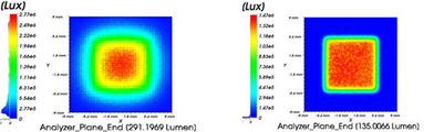
도 2는 양자점 코팅층의 표면에 요철구조의 패턴이 형성되어 있는 경우(좌)와 그렇지 않고 평탄면을 이루는 경우(우) 빛이 확산되는 정도를 보여주는 시뮬레이션 결과.
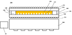
도 3은 본 발명의 다른 실시 예에 따른 색변환용 기판 및 이를 포함하는 디스플레이 장치를 개략적으로 나타낸 단면 모식도.
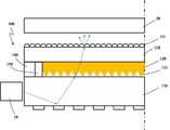
120: 양자점 코팅층 130, 240: 도광판
140: 밀봉재 150: 흡습제
210: 제1 박판유리 230: 제2 박판유리
111, 121, 211, 231: 패턴 10: 발광 다이오드
20: 디스플레이 패널
Claims (19)
- 박판유리;
상기 박판유리의 일면에 형성되는 양자점 코팅층;
상기 양자점 코팅층과 마주하게 배치되고, 측방으로는 발광 다이오드가 배치되는 도광판; 및
상기 박판유리와 상기 도광판 사이에 형성되어, 상기 양자점 코팅층을 외부와 차단시키는 밀봉재;
를 포함하는 것을 특징으로 하는 색변환용 기판.
- 제1항에 있어서,
상기 도광판과 마주하는 상기 양자점 코팅층의 표면에는 요철 구조의 패턴이 형성되어 있는 것을 특징으로 하는 색변환용 기판.
- 제1항에 있어서,
상기 박판유리의 타면에는 요철 구조의 패턴이 형성되어 있는 것을 특징으로 하는 색변환용 기판.
- 제1항에 있어서,
상기 도광판은 유리 도광판 또는 폴리머 도광판으로 이루어진 것을 특징으로 하는 색변환용 기판.
- 제4항에 있어서,
상기 도광판이 유리 도광판으로 이루어진 경우, 상기 밀봉재는 프릿으로 이루어지고, 상기 도광판이 폴리머 도광판으로 이루어진 경우, 상기 밀봉재는 에폭시로 이루어지는 것을 특징으로 하는 색변환용 기판.
- 제1항에 있어서,
상기 양자점 코팅층과 상기 밀봉재 사이에 배치되는 흡습제를 더 포함하는 것을 특징으로 하는 색변환용 기판.
- 제1 박판유리;
상기 제1 박판유리 하면에 형성되는 양자점 코팅층;
상기 양자점 코팅층 하면에 밀착되는 제2 박판유리;
상기 제1 박판유리와 상기 제2 박판유리 사이에 형성되어, 상기 양자점 코팅층을 외부와 차단시키는 밀봉재; 및
상기 제2 박판유리 하측에 배치되고, 측방으로는 발광 다이오드가 배치되는 도광판;
을 포함하는 것을 특징으로 하는 색변환용 기판.
- 제7항에 있어서,
상기 양자점 코팅층의 하면에는 요철 구조의 패턴이 형성되어 있는 것을 특징으로 하는 색변환용 기판.
- 제7항에 있어서,
상기 제1 박판유리의 상면에는 요철 구조의 패턴이 형성되어 있는 것을 특징으로 하는 색변환용 기판.
- 제7항에 있어서,
상기 제2 박판유리의 하면에는 요철 구조의 패턴이 형성되어 있는 것을 특징으로 하는 색변환용 기판.
- 제7항에 있어서,
상기 밀봉재는 프릿으로 이루어진 것을 특징으로 하는 색변환용 기판.
- 제7항에 있어서,
상기 양자점 코팅층과 상기 밀봉재 사이에 배치되는 흡습제를 더 포함하는 것을 특징으로 하는 색변환용 기판.
- 제1항 또는 제7항에 따른 색변환용 기판;
상기 색변환용 기판의 전방에 배치되는 디스플레이 패널; 및
상기 색변환용 기판의 도광판 측방에 배치되어, 상기 색변환용 기판과 측면 발광형 백라이트 유닛을 이루는 발광 다이오드;
를 포함하는 것을 특징으로 하는 디스플레이 장치.
- 제13항에 있어서,
상기 디스플레이 패널은 LCD 패널인 것을 특징으로 하는 디스플레이 장치.
- 양자점이 포함되어 있는 페이스트를 박판유리 상에 코팅하여 양자점 코팅층을 형성하는 제1 단계;
다른 박판유리 또는 도광판을 상기 박판유리와 대향되고 상기 양자점 코팅층과 마주하게 배치하는 제2 단계; 및
상기 박판유리와 상기 다른 박판유리의 마주하는 면 테두리 또는 상기 박판유리와 상기 도광판의 마주하는 면 테두리를 밀봉재를 매개로 밀봉하는 제3 단계;
를 포함하는 것을 특징으로 하는 색변환용 기판 제조방법.
- 제15항에 있어서,
상기 제1 단계에서는 상기 페이스트의 경화 정도를 조절하여, 상기 양자점 코팅층의 표면에 요철 구조의 패턴을 형성하는 것을 특징으로 하는 색변환용 기판 제조방법.
- 제15항에 있어서,
상기 밀봉재는 상기 제1 단계에서 상기 박판유리에 도포하거나 상기 제2 단계에서 상기 다른 박판유리 또는 상기 도광판에 도포하는 것을 특징으로 하는 색변환용 기판 제조방법.
- 제15항에 있어서,
상기 밀봉재로는 프릿 또는 에폭시를 사용하는 것을 특징으로 하는 색변환용 기판 제조방법.
- 제15항에 있어서,
상기 제2 단계 진행 전, 상기 양자점 코팅층 둘레를 따라 흡습제를 배치하는 것을 특징으로 하는 색변환용 기판 제조방법.
Priority Applications (7)
| Application Number | Priority Date | Filing Date | Title |
|---|---|---|---|
| KR1020140130971A KR20160038325A (ko) | 2014-09-30 | 2014-09-30 | 색변환용 기판, 그 제조방법 및 이를 포함하는 디스플레이 장치 |
| CN201580052979.XA CN107077028A (zh) | 2014-09-30 | 2015-08-07 | 用于颜色转换的基板、其制造方法以及包括其的显示装置 |
| US15/515,873 US10215907B2 (en) | 2014-09-30 | 2015-08-07 | Substrate for color conversion, manufacturing method therefor, and display device comprising same |
| JP2017517016A JP6623427B2 (ja) | 2014-09-30 | 2015-08-07 | 色変換用基板、その製造方法、及びそれを含むディスプレイ装置 |
| EP15848034.3A EP3203280A4 (en) | 2014-09-30 | 2015-08-07 | Substrate for color conversion, manufacturing method therefor, and display device comprising same |
| PCT/KR2015/008278 WO2016052856A1 (ko) | 2014-09-30 | 2015-08-07 | 색변환용 기판, 그 제조방법 및 이를 포함하는 디스플레이 장치 |
| TW104131995A TWI604239B (zh) | 2014-09-30 | 2015-09-30 | 顏色轉換基板、其製造方法及包含其之顯示裝置 |
Applications Claiming Priority (1)
| Application Number | Priority Date | Filing Date | Title |
|---|---|---|---|
| KR1020140130971A KR20160038325A (ko) | 2014-09-30 | 2014-09-30 | 색변환용 기판, 그 제조방법 및 이를 포함하는 디스플레이 장치 |
Publications (1)
| Publication Number | Publication Date |
|---|---|
| KR20160038325A true KR20160038325A (ko) | 2016-04-07 |
Family
ID=55630848
Family Applications (1)
| Application Number | Title | Priority Date | Filing Date |
|---|---|---|---|
| KR1020140130971A Ceased KR20160038325A (ko) | 2014-09-30 | 2014-09-30 | 색변환용 기판, 그 제조방법 및 이를 포함하는 디스플레이 장치 |
Country Status (7)
| Country | Link |
|---|---|
| US (1) | US10215907B2 (ko) |
| EP (1) | EP3203280A4 (ko) |
| JP (1) | JP6623427B2 (ko) |
| KR (1) | KR20160038325A (ko) |
| CN (1) | CN107077028A (ko) |
| TW (1) | TWI604239B (ko) |
| WO (1) | WO2016052856A1 (ko) |
Cited By (4)
| Publication number | Priority date | Publication date | Assignee | Title |
|---|---|---|---|---|
| CN108121112A (zh) * | 2016-11-30 | 2018-06-05 | 三星显示有限公司 | 背光单元、显示设备及显示设备的制造方法 |
| US10606123B2 (en) | 2017-08-29 | 2020-03-31 | Samsung Display Co., Ltd. | Display device having a light conversion member and method for fabricating the same |
| US11675231B2 (en) | 2018-12-19 | 2023-06-13 | Samsung Display Co., Ltd. | Composition for light conversion layer, light conversion layer and electronic device including the same |
| US11693172B2 (en) | 2018-04-10 | 2023-07-04 | Samsung Display Co., Ltd. | Backlight unit, display apparatus including the same, and manufacturing method thereof |
Families Citing this family (17)
| Publication number | Priority date | Publication date | Assignee | Title |
|---|---|---|---|---|
| DE102014117983A1 (de) * | 2014-12-05 | 2016-06-09 | Osram Opto Semiconductors Gmbh | Konversionselement, optoelektronisches Halbleiterbauelement und Verfahren zur Herstellung von Konversionselementen |
| KR102260013B1 (ko) * | 2014-12-10 | 2021-06-04 | 삼성디스플레이 주식회사 | 표시 장치 및 이의 제조 방법 |
| WO2016159366A1 (ja) * | 2015-04-02 | 2016-10-06 | 凸版印刷株式会社 | 量子ドット保護フィルム並びにこれを用いて得られる波長変換シート及びバックライトユニット |
| CN105810796A (zh) * | 2016-04-21 | 2016-07-27 | 深圳市华星光电技术有限公司 | 一种量子点材料玻璃板及其制作方法 |
| CN108196336B (zh) * | 2018-01-02 | 2020-06-30 | 京东方科技集团股份有限公司 | 一种导光板、背光模组、显示装置 |
| US20190219874A1 (en) * | 2018-01-16 | 2019-07-18 | Huizhou China Star Optoelectronics Technology Co., Ltd. | Backlight module and display device |
| JP6952203B2 (ja) | 2018-03-13 | 2021-10-20 | アップル インコーポレイテッドApple Inc. | 直接式バックライトユニットを有するディスプレイ |
| KR102537268B1 (ko) * | 2018-04-23 | 2023-05-30 | 삼성디스플레이 주식회사 | 표시 장치 |
| US10524666B2 (en) * | 2018-05-09 | 2020-01-07 | Inner Ray, Inc. | White excitation light generating device and white excitation light generating method |
| CN108807619A (zh) * | 2018-06-05 | 2018-11-13 | 福州大学 | 一种基于发光材料的qdef显示装置 |
| CN109755268A (zh) * | 2018-12-29 | 2019-05-14 | 武汉华星光电技术有限公司 | 一种色转换层及其制作方法、显示面板 |
| CN109499837B (zh) | 2018-12-29 | 2023-08-29 | 新疆天研种子机械工程技术研究中心(有限公司) | 一种辣椒清选分离系统 |
| WO2021240655A1 (ja) * | 2020-05-26 | 2021-12-02 | シャープ株式会社 | 発光素子及び発光素子の製造方法 |
| US11526051B2 (en) | 2021-04-16 | 2022-12-13 | Apple Inc. | Displays with direct-lit backlight units |
| US11592706B2 (en) | 2021-04-16 | 2023-02-28 | Apple Inc. | Displays with direct-lit backlight units |
| US11874559B2 (en) | 2021-09-23 | 2024-01-16 | Apple Inc. | Display modules with direct-lit backlight units |
| KR102927440B1 (ko) * | 2022-06-09 | 2026-02-12 | 삼성에스디아이 주식회사 | 디스플레이 장치 |
Family Cites Families (25)
| Publication number | Priority date | Publication date | Assignee | Title |
|---|---|---|---|---|
| KR20040090667A (ko) * | 2003-04-18 | 2004-10-26 | 삼성전기주식회사 | 디스플레이용 라이트 유닛 |
| KR100735148B1 (ko) * | 2004-11-22 | 2007-07-03 | (주)케이디티 | 백라이트 장치용 광 여기 확산시트, 이를 이용한액정표시용 백라이트 장치 |
| JP4955422B2 (ja) * | 2006-03-08 | 2012-06-20 | 三菱電機株式会社 | 発光装置 |
| ITMI20071238A1 (it) * | 2007-06-20 | 2008-12-21 | Getters Spa | Led bianchi o ultravioletti contenenti un sistema getter |
| KR101730164B1 (ko) * | 2007-07-18 | 2017-04-25 | 삼성전자주식회사 | 고체 조명에 유용한 양자점-기반 광 시트 |
| JP2009231273A (ja) * | 2008-02-27 | 2009-10-08 | Seiko Instruments Inc | 照明装置及びこれを備える表示装置 |
| JP5418762B2 (ja) * | 2008-04-25 | 2014-02-19 | ソニー株式会社 | 発光装置および表示装置 |
| KR101728575B1 (ko) * | 2009-10-07 | 2017-04-19 | 큐디 비젼, 인크. | 양자점을 포함하는 소자 |
| KR101154368B1 (ko) * | 2010-09-27 | 2012-06-15 | 엘지이노텍 주식회사 | 광변환부재 제조방법 및 그 제조방법으로 제조된 광변환부재를 포함하는 백라이트 유닛 |
| KR101210158B1 (ko) * | 2010-11-04 | 2012-12-07 | 엘지이노텍 주식회사 | 표시장치 및 광 변환 부재 |
| EP3540300B1 (en) * | 2010-11-10 | 2024-05-08 | Shoei Chemical Inc. | Quantum dot films, lighting devices, and lighting methods |
| KR20120088273A (ko) * | 2011-01-31 | 2012-08-08 | 엘지이노텍 주식회사 | 백라이트 유닛 및 그 제조 방법 |
| KR101210180B1 (ko) * | 2011-04-21 | 2012-12-07 | 엘지이노텍 주식회사 | 광학 부재 및 이의 제조방법 |
| KR101221921B1 (ko) * | 2011-07-05 | 2013-01-15 | 엘지전자 주식회사 | 이동 단말기 |
| KR20130009020A (ko) * | 2011-07-14 | 2013-01-23 | 엘지이노텍 주식회사 | 광학 부재, 이를 포함하는 표시장치 및 이의 제조방법 |
| KR101893494B1 (ko) * | 2011-07-18 | 2018-08-30 | 엘지이노텍 주식회사 | 광학 부재 및 이를 포함하는 표시장치 |
| JP2013033833A (ja) * | 2011-08-01 | 2013-02-14 | Panasonic Corp | 波長変換膜及びそれを用いた発光装置並びに照明装置 |
| KR101338695B1 (ko) * | 2012-04-27 | 2013-12-06 | 엘지이노텍 주식회사 | 표시 장치, 광 변환 부재 및 광 변환 부재 제조 방법 |
| WO2014024218A1 (ja) * | 2012-08-06 | 2014-02-13 | パナソニック株式会社 | 蛍光体光学素子、その製造方法及び光源装置 |
| KR101426448B1 (ko) | 2012-11-09 | 2014-08-05 | 주식회사 엘엠에스 | 나노 복합체, 이를 포함하는 광학 부재 및 백라이트 유닛 |
| CN104019401A (zh) * | 2013-02-28 | 2014-09-03 | 联想(北京)有限公司 | 一种背光模组、双显屏结构以及电子设备 |
| WO2014147690A1 (ja) * | 2013-03-18 | 2014-09-25 | 富士通株式会社 | モジュール型データセンター |
| KR102126176B1 (ko) * | 2014-02-05 | 2020-06-25 | 삼성디스플레이 주식회사 | 파장 변환 부재 및 그 제조 방법, 및 이를 포함하는 백라이트 어셈블리 |
| KR102140630B1 (ko) * | 2014-02-11 | 2020-08-04 | 삼성디스플레이 주식회사 | 파장 변환 부재 및 그 제조 방법, 및 이를 포함하는 백라이트 어셈블리 |
| US9513426B2 (en) * | 2014-10-22 | 2016-12-06 | Industrial Technology Research Institute | Light down conversion film and display backlight unit using the same |
-
2014
- 2014-09-30 KR KR1020140130971A patent/KR20160038325A/ko not_active Ceased
-
2015
- 2015-08-07 CN CN201580052979.XA patent/CN107077028A/zh active Pending
- 2015-08-07 WO PCT/KR2015/008278 patent/WO2016052856A1/ko not_active Ceased
- 2015-08-07 US US15/515,873 patent/US10215907B2/en active Active
- 2015-08-07 JP JP2017517016A patent/JP6623427B2/ja active Active
- 2015-08-07 EP EP15848034.3A patent/EP3203280A4/en not_active Withdrawn
- 2015-09-30 TW TW104131995A patent/TWI604239B/zh active
Cited By (5)
| Publication number | Priority date | Publication date | Assignee | Title |
|---|---|---|---|---|
| CN108121112A (zh) * | 2016-11-30 | 2018-06-05 | 三星显示有限公司 | 背光单元、显示设备及显示设备的制造方法 |
| KR20180062497A (ko) * | 2016-11-30 | 2018-06-11 | 삼성디스플레이 주식회사 | 백라이트 유닛, 표시 장치 및 표시 장치의 제조 방법 |
| US10606123B2 (en) | 2017-08-29 | 2020-03-31 | Samsung Display Co., Ltd. | Display device having a light conversion member and method for fabricating the same |
| US11693172B2 (en) | 2018-04-10 | 2023-07-04 | Samsung Display Co., Ltd. | Backlight unit, display apparatus including the same, and manufacturing method thereof |
| US11675231B2 (en) | 2018-12-19 | 2023-06-13 | Samsung Display Co., Ltd. | Composition for light conversion layer, light conversion layer and electronic device including the same |
Also Published As
| Publication number | Publication date |
|---|---|
| WO2016052856A1 (ko) | 2016-04-07 |
| JP6623427B2 (ja) | 2019-12-25 |
| EP3203280A1 (en) | 2017-08-09 |
| US10215907B2 (en) | 2019-02-26 |
| CN107077028A (zh) | 2017-08-18 |
| TW201626009A (zh) | 2016-07-16 |
| EP3203280A4 (en) | 2018-05-02 |
| JP2017532600A (ja) | 2017-11-02 |
| TWI604239B (zh) | 2017-11-01 |
| US20170299792A1 (en) | 2017-10-19 |
Similar Documents
| Publication | Publication Date | Title |
|---|---|---|
| JP6623427B2 (ja) | 色変換用基板、その製造方法、及びそれを含むディスプレイ装置 | |
| JP6276557B2 (ja) | Led発光装置 | |
| KR101555954B1 (ko) | 발광 다이오드의 색변환용 기판 및 그 제조방법 | |
| US9905542B2 (en) | LED light bar manufacturing method and LED light bar | |
| JP2015079805A (ja) | 発光装置 | |
| JP6253949B2 (ja) | Led発光装置 | |
| JP6282438B2 (ja) | 半導体発光装置 | |
| KR20170016815A (ko) | 발광 디바이스 | |
| JP6427816B2 (ja) | 発光ダイオードの色変換用基板及びその製造方法 | |
| KR101549406B1 (ko) | 발광 다이오드의 색변환용 기판 및 그 제조방법 | |
| JP2008205170A (ja) | 発光半導体デバイス | |
| TW201624775A (zh) | 用於發光二極體之顏色轉換基板及其製造方法 | |
| JP4943005B2 (ja) | 薄型発光ダイオードランプとその製造方法 | |
| CN110676364B (zh) | 一种四面出光蓝光波导面发光结构 | |
| JP2017135130A (ja) | 発光装置 | |
| WO2015194297A1 (ja) | 発光デバイス、波長変換部材及び波長変換部材の製造方法 | |
| KR20150034040A (ko) | 백라이트 패널 어셈블리 | |
| TWI619269B (zh) | 發光二極體封裝結構 | |
| JP2013098194A (ja) | 発光装置 | |
| JPWO2015194296A1 (ja) | 発光デバイス | |
| TWM544123U (zh) | 發光二極體封裝結構 | |
| KR102475623B1 (ko) | 발광 장치 | |
| WO2014057752A1 (ja) | 発光素子およびこれを備えた発光装置 | |
| KR20160096453A (ko) | 발광소자 패키지를 구비하는 디스플레이 장치 |
Legal Events
| Date | Code | Title | Description |
|---|---|---|---|
| A201 | Request for examination | ||
| PA0109 | Patent application |
Patent event code: PA01091R01D Comment text: Patent Application Patent event date: 20140930 |
|
| PA0201 | Request for examination | ||
| E902 | Notification of reason for refusal | ||
| PE0902 | Notice of grounds for rejection |
Comment text: Notification of reason for refusal Patent event date: 20160112 Patent event code: PE09021S01D |
|
| AMND | Amendment | ||
| PG1501 | Laying open of application | ||
| E601 | Decision to refuse application | ||
| PE0601 | Decision on rejection of patent |
Patent event date: 20160713 Comment text: Decision to Refuse Application Patent event code: PE06012S01D Patent event date: 20160112 Comment text: Notification of reason for refusal Patent event code: PE06011S01I |
|
| AMND | Amendment | ||
| PX0901 | Re-examination |
Patent event code: PX09011S01I Patent event date: 20160713 Comment text: Decision to Refuse Application Patent event code: PX09012R01I Patent event date: 20160314 Comment text: Amendment to Specification, etc. |
|
| PX0601 | Decision of rejection after re-examination |
Comment text: Decision to Refuse Application Patent event code: PX06014S01D Patent event date: 20160908 Comment text: Amendment to Specification, etc. Patent event code: PX06012R01I Patent event date: 20160809 Comment text: Decision to Refuse Application Patent event code: PX06011S01I Patent event date: 20160713 Comment text: Amendment to Specification, etc. Patent event code: PX06012R01I Patent event date: 20160314 Comment text: Notification of reason for refusal Patent event code: PX06013S01I Patent event date: 20160112 |
|
| J201 | Request for trial against refusal decision | ||
| PJ0201 | Trial against decision of rejection |
Patent event date: 20161010 Comment text: Request for Trial against Decision on Refusal Patent event code: PJ02012R01D Patent event date: 20160908 Comment text: Decision to Refuse Application Patent event code: PJ02011S01I Patent event date: 20160713 Comment text: Decision to Refuse Application Patent event code: PJ02011S01I Appeal kind category: Appeal against decision to decline refusal Appeal identifier: 2016101005863 Request date: 20161010 |
|
| J301 | Trial decision |
Free format text: TRIAL NUMBER: 2016101005863; TRIAL DECISION FOR APPEAL AGAINST DECISION TO DECLINE REFUSAL REQUESTED 20161010 Effective date: 20180906 |
|
| PJ1301 | Trial decision |
Patent event code: PJ13011S01D Patent event date: 20180906 Comment text: Trial Decision on Objection to Decision on Refusal Appeal kind category: Appeal against decision to decline refusal Request date: 20161010 Decision date: 20180906 Appeal identifier: 2016101005863 |