KR20160042008A - 메트롤로지 방법 및 장치, 리소그래피 시스템 및 디바이스 제조 방법 - Google Patents
메트롤로지 방법 및 장치, 리소그래피 시스템 및 디바이스 제조 방법 Download PDFInfo
- Publication number
- KR20160042008A KR20160042008A KR1020167005967A KR20167005967A KR20160042008A KR 20160042008 A KR20160042008 A KR 20160042008A KR 1020167005967 A KR1020167005967 A KR 1020167005967A KR 20167005967 A KR20167005967 A KR 20167005967A KR 20160042008 A KR20160042008 A KR 20160042008A
- Authority
- KR
- South Korea
- Prior art keywords
- overlay
- target structure
- measurements
- target
- asymmetry
- Prior art date
- Legal status (The legal status is an assumption and is not a legal conclusion. Google has not performed a legal analysis and makes no representation as to the accuracy of the status listed.)
- Granted
Links
Images







Classifications
-
- G—PHYSICS
- G03—PHOTOGRAPHY; CINEMATOGRAPHY; ANALOGOUS TECHNIQUES USING WAVES OTHER THAN OPTICAL WAVES; ELECTROGRAPHY; HOLOGRAPHY
- G03F—PHOTOMECHANICAL PRODUCTION OF TEXTURED OR PATTERNED SURFACES, e.g. FOR PRINTING, FOR PROCESSING OF SEMICONDUCTOR DEVICES; MATERIALS THEREFOR; ORIGINALS THEREFOR; APPARATUS SPECIALLY ADAPTED THEREFOR
- G03F7/00—Photomechanical, e.g. photolithographic, production of textured or patterned surfaces, e.g. printing surfaces; Materials therefor, e.g. comprising photoresists; Apparatus specially adapted therefor
- G03F7/70—Microphotolithographic exposure; Apparatus therefor
- G03F7/70483—Information management; Active and passive control; Testing; Wafer monitoring, e.g. pattern monitoring
- G03F7/70605—Workpiece metrology
- G03F7/70616—Monitoring the printed patterns
- G03F7/70633—Overlay, i.e. relative alignment between patterns printed by separate exposures in different layers, or in the same layer in multiple exposures or stitching
-
- G—PHYSICS
- G03—PHOTOGRAPHY; CINEMATOGRAPHY; ANALOGOUS TECHNIQUES USING WAVES OTHER THAN OPTICAL WAVES; ELECTROGRAPHY; HOLOGRAPHY
- G03F—PHOTOMECHANICAL PRODUCTION OF TEXTURED OR PATTERNED SURFACES, e.g. FOR PRINTING, FOR PROCESSING OF SEMICONDUCTOR DEVICES; MATERIALS THEREFOR; ORIGINALS THEREFOR; APPARATUS SPECIALLY ADAPTED THEREFOR
- G03F1/00—Originals for photomechanical production of textured or patterned surfaces, e.g., masks, photo-masks, reticles; Mask blanks or pellicles therefor; Containers specially adapted therefor; Preparation thereof
- G03F1/68—Preparation processes not covered by groups G03F1/20 - G03F1/50
- G03F1/72—Repair or correction of mask defects
-
- G—PHYSICS
- G03—PHOTOGRAPHY; CINEMATOGRAPHY; ANALOGOUS TECHNIQUES USING WAVES OTHER THAN OPTICAL WAVES; ELECTROGRAPHY; HOLOGRAPHY
- G03F—PHOTOMECHANICAL PRODUCTION OF TEXTURED OR PATTERNED SURFACES, e.g. FOR PRINTING, FOR PROCESSING OF SEMICONDUCTOR DEVICES; MATERIALS THEREFOR; ORIGINALS THEREFOR; APPARATUS SPECIALLY ADAPTED THEREFOR
- G03F7/00—Photomechanical, e.g. photolithographic, production of textured or patterned surfaces, e.g. printing surfaces; Materials therefor, e.g. comprising photoresists; Apparatus specially adapted therefor
- G03F7/70—Microphotolithographic exposure; Apparatus therefor
- G03F7/70483—Information management; Active and passive control; Testing; Wafer monitoring, e.g. pattern monitoring
- G03F7/70491—Information management, e.g. software; Active and passive control, e.g. details of controlling exposure processes or exposure tool monitoring processes
- G03F7/70508—Data handling in all parts of the microlithographic apparatus, e.g. handling pattern data for addressable masks or data transfer to or from different components within the exposure apparatus
-
- G—PHYSICS
- G03—PHOTOGRAPHY; CINEMATOGRAPHY; ANALOGOUS TECHNIQUES USING WAVES OTHER THAN OPTICAL WAVES; ELECTROGRAPHY; HOLOGRAPHY
- G03F—PHOTOMECHANICAL PRODUCTION OF TEXTURED OR PATTERNED SURFACES, e.g. FOR PRINTING, FOR PROCESSING OF SEMICONDUCTOR DEVICES; MATERIALS THEREFOR; ORIGINALS THEREFOR; APPARATUS SPECIALLY ADAPTED THEREFOR
- G03F7/00—Photomechanical, e.g. photolithographic, production of textured or patterned surfaces, e.g. printing surfaces; Materials therefor, e.g. comprising photoresists; Apparatus specially adapted therefor
- G03F7/70—Microphotolithographic exposure; Apparatus therefor
- G03F7/70483—Information management; Active and passive control; Testing; Wafer monitoring, e.g. pattern monitoring
- G03F7/70591—Testing optical components
- G03F7/706—Aberration measurement
-
- G—PHYSICS
- G03—PHOTOGRAPHY; CINEMATOGRAPHY; ANALOGOUS TECHNIQUES USING WAVES OTHER THAN OPTICAL WAVES; ELECTROGRAPHY; HOLOGRAPHY
- G03F—PHOTOMECHANICAL PRODUCTION OF TEXTURED OR PATTERNED SURFACES, e.g. FOR PRINTING, FOR PROCESSING OF SEMICONDUCTOR DEVICES; MATERIALS THEREFOR; ORIGINALS THEREFOR; APPARATUS SPECIALLY ADAPTED THEREFOR
- G03F7/00—Photomechanical, e.g. photolithographic, production of textured or patterned surfaces, e.g. printing surfaces; Materials therefor, e.g. comprising photoresists; Apparatus specially adapted therefor
- G03F7/70—Microphotolithographic exposure; Apparatus therefor
- G03F7/70483—Information management; Active and passive control; Testing; Wafer monitoring, e.g. pattern monitoring
- G03F7/70605—Workpiece metrology
- G03F7/706835—Metrology information management or control
- G03F7/706839—Modelling, e.g. modelling scattering or solving inverse problems
-
- G—PHYSICS
- G03—PHOTOGRAPHY; CINEMATOGRAPHY; ANALOGOUS TECHNIQUES USING WAVES OTHER THAN OPTICAL WAVES; ELECTROGRAPHY; HOLOGRAPHY
- G03F—PHOTOMECHANICAL PRODUCTION OF TEXTURED OR PATTERNED SURFACES, e.g. FOR PRINTING, FOR PROCESSING OF SEMICONDUCTOR DEVICES; MATERIALS THEREFOR; ORIGINALS THEREFOR; APPARATUS SPECIALLY ADAPTED THEREFOR
- G03F7/00—Photomechanical, e.g. photolithographic, production of textured or patterned surfaces, e.g. printing surfaces; Materials therefor, e.g. comprising photoresists; Apparatus specially adapted therefor
- G03F7/70—Microphotolithographic exposure; Apparatus therefor
- G03F7/70483—Information management; Active and passive control; Testing; Wafer monitoring, e.g. pattern monitoring
- G03F7/70605—Workpiece metrology
- G03F7/706843—Metrology apparatus
-
- H01L21/0274—
-
- H01L22/12—
-
- H—ELECTRICITY
- H10—SEMICONDUCTOR DEVICES; ELECTRIC SOLID-STATE DEVICES NOT OTHERWISE PROVIDED FOR
- H10P—GENERIC PROCESSES OR APPARATUS FOR THE MANUFACTURE OR TREATMENT OF DEVICES COVERED BY CLASS H10
- H10P74/00—Testing or measuring during manufacture or treatment of wafers, substrates or devices
- H10P74/20—Testing or measuring during manufacture or treatment of wafers, substrates or devices characterised by the properties tested or measured, e.g. structural or electrical properties
- H10P74/203—Structural properties, e.g. testing or measuring thicknesses, line widths, warpage, bond strengths or physical defects
-
- H—ELECTRICITY
- H10—SEMICONDUCTOR DEVICES; ELECTRIC SOLID-STATE DEVICES NOT OTHERWISE PROVIDED FOR
- H10P—GENERIC PROCESSES OR APPARATUS FOR THE MANUFACTURE OR TREATMENT OF DEVICES COVERED BY CLASS H10
- H10P74/00—Testing or measuring during manufacture or treatment of wafers, substrates or devices
- H10P74/27—Structural arrangements therefor
-
- H—ELECTRICITY
- H10—SEMICONDUCTOR DEVICES; ELECTRIC SOLID-STATE DEVICES NOT OTHERWISE PROVIDED FOR
- H10P—GENERIC PROCESSES OR APPARATUS FOR THE MANUFACTURE OR TREATMENT OF DEVICES COVERED BY CLASS H10
- H10P76/00—Manufacture or treatment of masks on semiconductor bodies, e.g. by lithography or photolithography
- H10P76/20—Manufacture or treatment of masks on semiconductor bodies, e.g. by lithography or photolithography of masks comprising organic materials
- H10P76/204—Manufacture or treatment of masks on semiconductor bodies, e.g. by lithography or photolithography of masks comprising organic materials of organic photoresist masks
- H10P76/2041—Photolithographic processes
Landscapes
- Physics & Mathematics (AREA)
- General Physics & Mathematics (AREA)
- Exposure And Positioning Against Photoresist Photosensitive Materials (AREA)
- Length Measuring Devices By Optical Means (AREA)
- Container, Conveyance, Adherence, Positioning, Of Wafer (AREA)
Abstract
Description
도 1은 본 발명의 일 실시예에 따른 리소그래피 장치를 도시하는 도면;
도 2는 본 발명의 일 실시예에 따른 리소그래피 셀 또는 클러스터를 도시하는 도면;
도 3a 내지 도 3d는 (a) 제 1 쌍의 조명 어퍼처들을 이용하여 본 발명의 실시예들에 따른 타겟들을 측정하는 데 사용되는 다크 필드 스케터로미터의 개략적인 다이어그램, (b) 주어진 방향의 조명에 대한 타겟 격자의 상세한 회절 스펙트럼, (c) 회절 기반 오버레이 측정들을 위해 스케터로미터를 이용함에 있어서 또 다른 조명 모드들을 제공하는 제 2 쌍의 조명 어퍼처들, 및 (d) 제 1 및 제 2 쌍의 어퍼처들을 조합한 제 3 쌍의 조명 어퍼처들을 포함하는 도면;
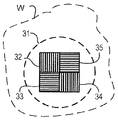
도 4는 알려진 형태의 다수 격자 타겟 및 기판 상의 측정 스폿의 윤곽(outline)을 도시하는 도면;
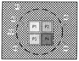
도 5는 도 3의 스케터로미터에서 얻어진 도 4의 타겟의 이미지를 도시하는 도면;
도 6은 도 3의 스케터로미터를 이용하고, 본 발명의 일 실시예를 형성하도록 구성가능한 오버레이 측정 방법의 단계들을 나타내는 흐름도;
도 7은 본 발명의 일 실시예에 따른, 도 6의 흐름도의 단계 S6에서 확장된 흐름도;
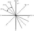
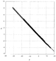
도 8은 피처 비대칭을 갖지 않는 오버레이 격자들의 A-에 대한 A+의 플롯(plot);
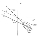
도 9는 본 발명의 제 1 실시예를 예시하는, 피처 비대칭을 갖는 오버레이 격자들의 A-에 대한 A+의 플롯;
도 10a 및 도 10b는 피처 비대칭을 갖지 않는 오버레이 격자, 및 본 발명의 제 2 실시예를 예시하는 피처 비대칭을 갖는 오버레이 격자의 A-에 대한 A+의 플롯;
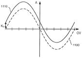
도 11은 피처 비대칭을 갖는 오버레이 격자의 오버레이에 대한 비대칭의 플롯;
도 12a는 큰 피처 비대칭을 갖는 오버레이 격자들의 A-에 대한 A+의 플롯;
도 12b는 본 발명의 제 3 실시예를 예시하는, 제 3 바이어스 및 큰 피처 비대칭을 포함하는 오버레이 격자의 A+-A0 대 A--A0의 플롯;
도 13은 본 발명의 제 3 실시예에서 사용될 수 있는 바이어스 방식을 갖는 복합 격자 구조체를 예시하는 도면;
도 14는 웨이퍼에 대한 오버레이의 그래픽 표현이고, 공정 비대칭에 대한 보정이 TE 및 TM 방사선으로 추산된 오버레이 간의 차이를 최소화한다는 것을 예시하는 도면;
도 14a 및 도 14b는 TE 방사선 및 TM 방사선을 각각 이용하여 웨이퍼에 걸쳐 수행된 보정되지 않은 오버레이 측정들의 표현들을 나타내는 도면;
도 14c는 도 14a 및 도 14b의 측정들 간의 차이들을 나타내는 도면;
도 14d 및 도 14e는 TE 방사선 및 TM 방사선을 각각 이용하여 웨이퍼에 걸쳐 수행되고, 본 발명의 일 실시예에 따라 보정된 오버레이 측정들의 표현들을 나타내는 도면; 및
도 14f는 도 14d 및 도 14e의 측정들 간의 차이들을 나타내는 도면이다.
동일한 참조 기호들이 대응하는 요소들을 전부 식별하는 도면들에 관련하여 아래에서 설명되는 상세한 설명으로부터 본 발명의 특징들 및 장점들이 더 분명해질 것이다. 도면들에서 동일한 참조 번호들은 일반적으로 동일하거나, 기능적으로 유사한, 및/또는 구조적으로 유사한 요소들을 나타낸다. 요소가 처음 나타나는 도면은 대응하는 참조 번호의 맨 앞자리 수(들)에 의해 나타내어진다.



Claims (32)
- 리소그래피 공정의 파라미터를 측정하는 방법에 있어서:
(a) 기판 상의 타겟 구조체들을 조명하는 단계 -상기 타겟 구조체들은 적어도 제 1 의도적 오버레이 바이어스(deliberate overlay bias)를 갖는 오버레이된 주기적 구조체(overlaid periodic structure)를 포함하는 제 1 타겟 구조체, 및 제 2 의도적 오버레이 바이어스를 갖는 오버레이된 주기적 구조체를 포함하는 제 2 타겟 구조체를 포함함- ; 및 각각의 타겟 구조체에 의해 산란되는 방사선을 검출하여, 각각의 타겟 구조체에 대해 (ⅰ) 상기 타겟 구조체에서의 의도적 오버레이 바이어스, (ⅱ) 상기 타겟 구조체의 형성 시 리소그래피 공정에서의 오버레이 오차, 및 (ⅲ) 상기 주기적 구조체들 중 1 이상에서의 피처 비대칭(feature asymmetry)으로 인한 기여들을 포함하는 전체 비대칭을 나타내는 비대칭 측정을 얻는 단계;
(b) 복수의 상이한 조명 조건들에 대해 단계(a)를 반복하여, 비대칭 측정 데이터를 얻는 단계;
(c) 상기 제 2 타겟 구조체의 비대칭 측정들에 대한 상기 제 1 타겟 구조체의 비대칭 측정들의 평면 표현(planar representation)에 선형 회귀 모델(linear regression model)을 피팅함으로써, 상기 비대칭 측정 데이터에 대한 회귀 분석을 수행하는 단계 -상기 선형 회귀 모델은 반드시 상기 평면 표현의 원점(origin)을 통해 피팅되지는 않음- ; 및
(d) 상기 선형 회귀 모델에 의해 형성되는 기울기(gradient)로부터 상기 오버레이 오차를 결정하는 단계
를 포함하는 리소그래피 공정의 파라미터 측정 방법. - 제 1 항에 있어서,
상기 선형 회귀 모델의 절편 항(intercept term)으로부터 상기 전체 비대칭 중 피처 비대칭으로 인한 기여를 결정하는 단계를 포함하는 리소그래피 공정의 파라미터 측정 방법. - 제 2 항에 있어서,
상기 전체 비대칭 중 피처 비대칭으로 인한 결정된 기여의 함수인 오버레이 보정을 결정하는 단계; 및
상기 오버레이 보정을 이용하여 상기 오버레이 오차를 보정하는 단계를 포함하는 리소그래피 공정의 파라미터 측정 방법. - 제 3 항에 있어서,
상기 기판 상의 복수의 상이한 위치들에 대해 오버레이 오차 측정들을 결정하기 위해 단계 (a) 내지 단계 (d)를 수행하는 단계 -각각의 위치에 대한 오버레이 오차 측정들은 TE 편광 방사선 및 TM 편광 방사선을 이용하여 얻어짐- ; 및
TE 편광 방사선을 이용하여 측정되는 경우에 측정된 오버레이 오차와 TM 편광 방사선을 이용하여 측정되는 경우에 측정된 오버레이 오차 간의 차이의 최소화를 수행함으로써 상기 오버레이 보정을 계산하는 단계를 포함하는 리소그래피 공정의 파라미터 측정 방법. - 제 1 항 내지 제 4 항 중 어느 한 항에 있어서,
상기 비대칭 측정들에 피팅되는 상기 선형 회귀 모델은 상기 원점의 구역에 놓이는 비대칭 측정 데이터에만 피팅되는 리소그래피 공정의 파라미터 측정 방법. - 제 5 항에 있어서,
복수의 조명 조건들로부터, 피처 비대칭이 측정된 전체 비대칭에 대한 최소 기여를 하는 1 이상의 최적 조명 조건들을 식별하는 단계를 포함하고, 상기 최적 조명 조건들은 측정된 비대칭들이 오프셋 라인 또는 그 부근에 놓이는 조건들로부터 선택되며, 상기 오프셋 라인은 상기 선형 회귀 모델에 의해 형성되지만, 상기 원점 상에 놓이도록 0(zero) 절편 항을 갖는 라인인 리소그래피 공정의 파라미터 측정 방법. - 제 6 항에 있어서,
상기 최적 조명 조건들은 상기 측정된 비대칭들이 상기 오프셋 라인 또는 그 부근에 놓이지 않는 측정된 비대칭들로부터 가장 멀리 있는 조건들로부터 선택되는 리소그래피 공정의 파라미터 측정 방법. - 제 6 항 또는 제 7 항에 있어서,
상기 최적 조명 조건들 중 1 이상을 이용하여 상기 기판 상의 구조체들의 후속 측정들을 수행하는 단계를 포함하는 리소그래피 공정의 파라미터 측정 방법. - 제 1 항 내지 제 8 항 중 어느 한 항에 있어서,
상기 제 1 의도적 오버레이 바이어스는 양(positive)의 오버레이 바이어스이고, 상기 제 2 의도적 오버레이 바이어스는 음(negative)의 오버레이 바이어스인 리소그래피 공정의 파라미터 측정 방법. - 제 9 항에 있어서,
상기 제 1 의도적 오버레이 바이어스 및 상기 제 2 의도적 오버레이 바이어스는 동일한 크기(magnitude)로 이루어지는 리소그래피 공정의 파라미터 측정 방법. - 제 1 항 내지 제 10 항 중 어느 한 항에 있어서,
단계 (d)는 피처 비대칭으로 인한 기여가 모든 오버레이 값들에 대해 일정하다는 가정으로 수행되는 리소그래피 공정의 파라미터 측정 방법. - 제 1 항 내지 제 10 항 중 어느 한 항에 있어서,
상기 타겟 구조체들은 의도적 오버레이 바이어스를 갖지 않는 제 3 타겟 구조체를 포함하고, 상기 방법은 상기 제 1 타겟 구조체 및 상기 제 3 타겟 구조체에 대해 단계 (b)에서 얻어진 비대칭 측정들 간의 차이, 및 상기 제 2 타겟 구조체 및 상기 제 3 타겟 구조체에 대해 단계 (b)에서 얻어진 비대칭 측정들 간의 차이로부터 상대적 비대칭 측정들을 결정하는 단계를 포함하는 리소그래피 공정의 파라미터 측정 방법. - 제 12 항에 있어서,
단계 (c)는 상기 제 2 타겟 구조체에 대한 비대칭 측정들과 상기 제 3 타겟 구조체에 대한 비대칭 측정들의 차이에 대한, 상기 제 1 타겟 구조체에 대한 비대칭 측정들과 상기 제 3 타겟 구조체에 대한 비대칭 측정들의 차이의 평면 표현에 선형 회귀 모델을 피팅하는 단계를 포함하는 리소그래피 공정의 파라미터 측정 방법. - 제 12 항 또는 제 13 항에 있어서,
단계 (d)는 피처 비대칭으로 인한 기여가 모든 오버레이 값들에 대해 일정하다는 가정 없이 수행되는 리소그래피 공정의 파라미터 측정 방법. - 제 1 항 내지 제 14 항 중 어느 한 항에 있어서,
기판 상에 상기 타겟 구조체들을 형성하기 위해 리소그래피 공정을 이용하는 초기 단계를 포함하는 리소그래피 공정의 파라미터 측정 방법. - 리소그래피 공정의 파라미터를 측정하는 검사 장치에 있어서,
복수의 타겟 구조체들을 갖는 기판에 대한 지지체 -상기 타겟 구조체들은 적어도 제 1 의도적 오버레이 바이어스를 갖는 오버레이된 주기적 구조체를 포함하는 제 1 타겟 구조체, 및 제 2 의도적 오버레이 바이어스를 갖는 오버레이된 주기적 구조체를 포함하는 제 2 타겟 구조체를 포함함- ;
상기 타겟들을 조명하도록 작동가능하고, 각각의 타겟에 의해 산란되는 방사선을 검출하여, 각각의 타겟 구조체 및 복수의 상이한 조명 조건들에 대해 (ⅰ) 상기 타겟 구조체에서의 의도적 오버레이 바이어스, (ⅱ) 상기 타겟 구조체의 형성 시 리소그래피 공정에서의 오버레이 오차, 및 (ⅲ) 상기 주기적 구조체들 중 1 이상에서의 피처 비대칭으로 인한 기여들을 포함하는 전체 비대칭을 나타내는 비대칭 측정을 얻기 위한 광학 시스템; 및
상기 제 2 타겟 구조체의 비대칭 측정들에 대한 상기 제 1 타겟 구조체의 비대칭 측정들의 평면 표현에 선형 회귀 모델을 피팅함으로써 비대칭 측정 데이터에 대한 회귀 분석을 수행하고 -상기 선형 회귀 모델은 반드시 상기 평면 표현의 원점을 통해 피팅되지는 않음- ; 상기 선형 회귀 모델에 의해 형성되는 기울기로부터 상기 오버레이 오차를 결정하도록 배치되는 프로세서
를 포함하는 검사 장치. - 제 16 항에 있어서,
상기 프로세서는 상기 선형 회귀 모델의 절편 항으로부터 상기 전체 비대칭 중 피처 비대칭으로 인한 기여를 결정하도록 작동가능한 검사 장치. - 제 17 항에 있어서,
상기 전체 비대칭 중 피처 비대칭으로 인한 결정된 기여의 함수인 오버레이 보정을 결정하고;
상기 오버레이 보정을 이용하여 상기 오버레이 오차를 결정하도록 작동가능한 검사 장치. - 제 18 항에 있어서,
상기 기판 상의 복수의 상이한 위치들에 대해 오버레이 오차 측정들을 결정하도록 단계 (a) 내지 단계 (d)를 수행하고 -각각의 위치에 대한 오버레이 오차 측정들은 TE 편광 방사선 및 TM 편광 방사선을 이용하여 얻어짐- ;
TE 편광 방사선을 이용하여 측정되는 경우에 측정된 오버레이 오차와 TM 편광 방사선을 이용하여 측정되는 경우에 측정된 오버레이 오차 간의 차이의 최소화를 수행함으로써 상기 오버레이 보정을 계산하도록 작동가능한 검사 장치. - 제 16 항 내지 제 19 항 중 어느 한 항에 있어서,
상기 프로세서는 상기 원점의 구역에 놓이는 비대칭 측정 데이터에만 상기 선형 회귀 모델을 피팅하도록 작동가능한 검사 장치. - 제 20 항에 있어서,
상기 프로세서는 복수의 조명 조건들로부터, 피처 비대칭이 측정된 전체 비대칭에 대한 최소 기여를 하는 1 이상의 최적 조명 조건들을 식별하도록 작동가능하고, 상기 최적 조명 조건들은 측정된 비대칭들이 오프셋 라인 또는 그 부근에 놓이는 조건들로부터 선택되며, 상기 오프셋 라인은 상기 선형 회귀 모델에 의해 형성되지만, 상기 원점 상에 놓이도록 0 절편 항을 갖는 라인인 검사 장치. - 제 21 항에 있어서,
상기 프로세서는 상기 측정된 비대칭들이 상기 오프셋 라인 또는 그 부근에 놓이지 않는 측정된 비대칭들로부터 가장 멀리 있는 조건들로부터 상기 최적 조명 조건들을 선택하도록 작동가능한 검사 장치. - 제 21 항 또는 제 22 항에 있어서,
상기 최적 조명 조건들 중 1 이상을 이용하여 상기 기판 상의 구조체들의 후속 측정들을 수행하도록 작동가능한 검사 장치. - 제 16 항 내지 제 23 항 중 어느 한 항에 있어서,
상기 제 1 의도적 오버레이 바이어스는 양의 오버레이 바이어스이고, 상기 제 2 의도적 오버레이 바이어스는 음의 오버레이 바이어스인 검사 장치. - 제 24 항에 있어서,
상기 제 1 의도적 오버레이 바이어스 및 상기 제 2 의도적 오버레이 바이어스는 동일한 크기로 이루어지는 검사 장치. - 제 16 항 내지 제 25 항 중 어느 한 항에 있어서,
상기 프로세서는 피처 비대칭으로 인한 기여가 모든 오버레이 값들에 대해 일정하다는 가정으로, 상기 선형 회귀 모델에 의해 형성되는 기울기로부터 상기 오버레이 오차를 결정하도록 작동가능한 검사 장치. - 제 16 항 내지 제 25 항 중 어느 한 항에 있어서,
상기 타겟 구조체들은 의도적 오버레이 바이어스를 갖지 않는 제 3 타겟 구조체를 포함하고, 상기 프로세서는 상기 제 1 타겟 구조체 및 상기 제 3 타겟 구조체에 대한 비대칭 측정들 간의 차이, 및 상기 제 2 타겟 구조체 및 상기 제 3 타겟 구조체에 대한 비대칭 측정들 간의 차이로부터 상대적 비대칭 측정들을 결정하도록 작동가능한 검사 장치. - 제 27 항에 있어서,
상기 프로세서는 상기 제 2 타겟 구조체에 대한 비대칭 측정들과 상기 제 3 타겟 구조체에 대한 비대칭 측정들의 차이에 대한, 상기 제 1 타겟 구조체에 대한 비대칭 측정들과 상기 제 3 타겟 구조체에 대한 비대칭 측정들의 차이의 평면 표현에 선형 회귀 모델을 피팅하도록 작동가능한 검사 장치. - 제 27 항 또는 제 28 항에 있어서,
상기 프로세서는 피처 비대칭으로 인한 기여가 모든 오버레이 값들에 대해 일정하다는 가정 없이, 상기 선형 회귀 모델에 의해 형성되는 기울기로부터 상기 오버레이 오차를 결정하도록 작동가능한 검사 장치. - 리소그래피 장치에 있어서,
제 16 항 내지 제 29 항 중 어느 한 항에 따른 검사 장치를 포함하며,
리소그래피 공정을 이용하여 일련의 기판들에 디바이스 패턴을 적용하고;
상기 일련의 기판들 중 1 이상에 타겟 구조체들을 적용하며;
제 1 항 내지 제 15 항 중 어느 한 항에 따른 파라미터 측정 방법을 이용하여 상기 타겟 구조체의 오버레이 파라미터를 측정하고;
상기 파라미터 측정 방법의 결과에 따라 후속 기판들에 대해 상기 리소그래피 공정을 제어하도록 작동가능한 리소그래피 장치. - 리소그래피 공정을 이용하여 일련의 기판들에 디바이스 패턴이 적용되는 디바이스들을 제조하는 방법에 있어서,
제 1 항 내지 제 15 항 중 어느 한 항에 따른 방법을 이용하여, 상기 기판들 중 적어도 하나에 상기 디바이스 패턴의 일부로서 또는 상기 디바이스 패턴 옆에 형성되는 적어도 하나의 주기적 구조체를 검사하는 단계; 및 검사 방법의 결과에 따라 후속 기판들에 대해 상기 리소그래피 공정을 제어하는 단계를 포함하는 디바이스 제조 방법. - 컴퓨터 프로그램 제품에 있어서,
비대칭 데이터에 대해, 제 1 항 내지 제 15 항 중 어느 한 항에 따른 방법의 처리 단계들 (c) 및 (d)를 프로세서가 수행하게 하는 기계-판독가능한 명령어들을 포함하며, 상기 비대칭 데이터는:
복수의 상이한 조명 조건들 하에 기판 상의 타겟 구조체들을 조명하고 -상기 타겟 구조체들은 적어도 제 1 의도적 오버레이 바이어스를 갖는 오버레이된 주기적 구조체를 포함하는 제 1 타겟 구조체, 및 제 2 의도적 오버레이 바이어스를 갖는 오버레이된 주기적 구조체를 포함하는 제 2 타겟 구조체를 포함함- ;
각각의 타겟 구조체에 의해 산란되는 방사선을 검출하여, 각각의 타겟 구조체에 대해 (ⅰ) 상기 타겟 구조체에서의 의도적 오버레이 바이어스, (ⅱ) 상기 타겟 구조체의 형성 시 리소그래피 공정에서의 오버레이 오차, 및 (ⅲ) 상기 주기적 구조체들 중 1 이상에서의 피처 비대칭으로 인한 기여들을 포함하는 전체 비대칭을 나타내는 비대칭 측정을 얻음으로써 얻어지는 컴퓨터 프로그램 제품.
Applications Claiming Priority (5)
| Application Number | Priority Date | Filing Date | Title |
|---|---|---|---|
| US201361863150P | 2013-08-07 | 2013-08-07 | |
| US61/863,150 | 2013-08-07 | ||
| US201461975312P | 2014-04-04 | 2014-04-04 | |
| US61/975,312 | 2014-04-04 | ||
| PCT/EP2014/065461 WO2015018625A1 (en) | 2013-08-07 | 2014-07-18 | Metrology method and apparatus, lithographic system and device manufacturing method |
Related Child Applications (1)
| Application Number | Title | Priority Date | Filing Date |
|---|---|---|---|
| KR1020187012297A Division KR102124204B1 (ko) | 2013-08-07 | 2014-07-18 | 메트롤로지 방법 및 장치, 리소그래피 시스템 및 디바이스 제조 방법 |
Publications (2)
| Publication Number | Publication Date |
|---|---|
| KR20160042008A true KR20160042008A (ko) | 2016-04-18 |
| KR101855243B1 KR101855243B1 (ko) | 2018-05-04 |
Family
ID=51211228
Family Applications (2)
| Application Number | Title | Priority Date | Filing Date |
|---|---|---|---|
| KR1020167005967A Active KR101855243B1 (ko) | 2013-08-07 | 2014-07-18 | 메트롤로지 방법 및 장치, 리소그래피 시스템 및 디바이스 제조 방법 |
| KR1020187012297A Active KR102124204B1 (ko) | 2013-08-07 | 2014-07-18 | 메트롤로지 방법 및 장치, 리소그래피 시스템 및 디바이스 제조 방법 |
Family Applications After (1)
| Application Number | Title | Priority Date | Filing Date |
|---|---|---|---|
| KR1020187012297A Active KR102124204B1 (ko) | 2013-08-07 | 2014-07-18 | 메트롤로지 방법 및 장치, 리소그래피 시스템 및 디바이스 제조 방법 |
Country Status (8)
| Country | Link |
|---|---|
| US (4) | US9910366B2 (ko) |
| JP (2) | JP6336068B2 (ko) |
| KR (2) | KR101855243B1 (ko) |
| CN (2) | CN105452962B (ko) |
| IL (1) | IL243854B (ko) |
| NL (1) | NL2013210A (ko) |
| TW (3) | TWI563345B (ko) |
| WO (1) | WO2015018625A1 (ko) |
Cited By (3)
| Publication number | Priority date | Publication date | Assignee | Title |
|---|---|---|---|---|
| KR20190007000A (ko) * | 2016-06-10 | 2019-01-21 | 아이엠이씨 브이제트더블유 | 반도체 제조 프로세스를 위한 계측 방법 및 장치 |
| KR20190051071A (ko) * | 2016-09-27 | 2019-05-14 | 에이에스엠엘 네델란즈 비.브이. | 계측 레시피 선택 |
| KR20200014829A (ko) * | 2017-06-30 | 2020-02-11 | 에이에스엠엘 네델란즈 비.브이. | 계측 파라미터 결정 및 계측 레시피 선택 |
Families Citing this family (83)
| Publication number | Priority date | Publication date | Assignee | Title |
|---|---|---|---|---|
| US9927718B2 (en) * | 2010-08-03 | 2018-03-27 | Kla-Tencor Corporation | Multi-layer overlay metrology target and complimentary overlay metrology measurement systems |
| US10890436B2 (en) | 2011-07-19 | 2021-01-12 | Kla Corporation | Overlay targets with orthogonal underlayer dummyfill |
| NL2011477A (en) * | 2012-10-10 | 2014-04-14 | Asml Netherlands Bv | Mark position measuring apparatus and method, lithographic apparatus and device manufacturing method. |
| WO2014062972A1 (en) * | 2012-10-18 | 2014-04-24 | Kla-Tencor Corporation | Symmetric target design in scatterometry overlay metrology |
| KR101855243B1 (ko) | 2013-08-07 | 2018-05-04 | 에이에스엠엘 네델란즈 비.브이. | 메트롤로지 방법 및 장치, 리소그래피 시스템 및 디바이스 제조 방법 |
| CN112698551B (zh) * | 2014-11-25 | 2024-04-23 | 科磊股份有限公司 | 分析及利用景观 |
| WO2016083076A1 (en) | 2014-11-26 | 2016-06-02 | Asml Netherlands B.V. | Metrology method, computer product and system |
| CN107430350B (zh) | 2015-02-04 | 2019-10-18 | Asml荷兰有限公司 | 计量方法和设备、计算机程序和光刻系统 |
| US11580274B2 (en) | 2015-04-10 | 2023-02-14 | Asml Netherlands B.V. | Method and apparatus for inspection and metrology |
| KR102048794B1 (ko) * | 2015-04-21 | 2020-01-08 | 에이에스엠엘 네델란즈 비.브이. | 계측 방법 및 장치, 컴퓨터 프로그램 및 리소그래피 시스템 |
| TWI656409B (zh) * | 2015-09-09 | 2019-04-11 | 美商克萊譚克公司 | 基於輔助電磁場之引入之一階散射測量疊加之新方法 |
| KR102351636B1 (ko) * | 2015-09-21 | 2022-01-13 | 케이엘에이 코포레이션 | 유연적 샘플링을 이용한 공정 제어 방법 및 시스템 |
| CN108431695B (zh) | 2015-12-24 | 2020-07-21 | Asml荷兰有限公司 | 控制图案形成过程的方法、器件制造方法、用于光刻设备的控制系统以及光刻设备 |
| KR102106937B1 (ko) | 2016-02-19 | 2020-05-07 | 에이에스엠엘 네델란즈 비.브이. | 구조체 측정 방법, 검사 장치, 리소그래피 시스템, 디바이스 제조 방법 및 그 안에 사용되는 파장-선택 필터 |
| JP6703612B2 (ja) | 2016-02-26 | 2020-06-03 | エーエスエムエル ネザーランズ ビー.ブイ. | 構造を測定する方法、検査装置、リソグラフィシステム、およびデバイス製造方法 |
| US10615084B2 (en) | 2016-03-01 | 2020-04-07 | Asml Netherlands B.V. | Method and apparatus to determine a patterning process parameter, associated with a change in a physical configuration, using measured pixel optical characteristic values |
| CN109073992B (zh) | 2016-04-22 | 2021-09-28 | Asml荷兰有限公司 | 堆叠差异的确定和使用堆叠差异的校正 |
| US10115621B2 (en) | 2016-05-13 | 2018-10-30 | Globalfoundries Inc. | Method for in-die overlay control using FEOL dummy fill layer |
| CN109478023B (zh) | 2016-07-15 | 2021-09-10 | Asml荷兰有限公司 | 用于量测目标场的设计的方法和设备 |
| US10048132B2 (en) * | 2016-07-28 | 2018-08-14 | Kla-Tencor Corporation | Simultaneous capturing of overlay signals from multiple targets |
| EP3293574A1 (en) | 2016-09-09 | 2018-03-14 | ASML Netherlands B.V. | Metrology method, apparatus and computer program |
| EP3299890A1 (en) | 2016-09-27 | 2018-03-28 | ASML Netherlands B.V. | Metrology recipe selection |
| KR102259091B1 (ko) * | 2016-11-10 | 2021-06-01 | 에이에스엠엘 네델란즈 비.브이. | 스택 차이를 이용한 설계 및 교정 |
| EP3333631A1 (en) | 2016-12-06 | 2018-06-13 | ASML Netherlands B.V. | Method of measuring a target, metrology apparatus, polarizer assembly |
| EP3333632A1 (en) | 2016-12-08 | 2018-06-13 | ASML Netherlands B.V. | Metrology apparatus |
| US10983005B2 (en) | 2016-12-15 | 2021-04-20 | Taiwan Semiconductor Manufacturing Co., Ltd. | Spectroscopic overlay metrology |
| EP3336607A1 (en) | 2016-12-16 | 2018-06-20 | ASML Netherlands B.V. | Method of measuring a property of a substrate, inspection apparatus, lithographic system and device manufacturing method |
| EP3358413A1 (en) * | 2017-02-02 | 2018-08-08 | ASML Netherlands B.V. | Metrology method, apparatus and computer program |
| US10656535B2 (en) * | 2017-03-31 | 2020-05-19 | Imec Vzw | Metrology method for a semiconductor manufacturing process |
| CN110546577B (zh) | 2017-04-28 | 2022-05-24 | Asml荷兰有限公司 | 计量方法和设备以及相关联的计算机程序 |
| WO2018202388A1 (en) | 2017-05-03 | 2018-11-08 | Asml Netherlands B.V. | Metrology parameter determination and metrology recipe selection |
| EP3399371A1 (en) | 2017-05-05 | 2018-11-07 | ASML Netherlands B.V. | Method of measuring a parameter of interest, device manufacturing method, metrology apparatus, and lithographic system |
| KR102432667B1 (ko) | 2017-05-15 | 2022-08-17 | 삼성전자주식회사 | 오버레이 보정방법 및 제어 시스템 |
| EP3422103A1 (en) | 2017-06-26 | 2019-01-02 | ASML Netherlands B.V. | Method of determining a performance parameter of a process |
| EP3435162A1 (en) * | 2017-07-28 | 2019-01-30 | ASML Netherlands B.V. | Metrology method and apparatus and computer program |
| EP3454126A1 (en) * | 2017-09-08 | 2019-03-13 | ASML Netherlands B.V. | Method for estimating overlay |
| WO2019048145A1 (en) * | 2017-09-11 | 2019-03-14 | Asml Netherlands B.V. | METROLOGY IN LITHOGRAPHIC PROCESSES |
| EP3462239A1 (en) * | 2017-09-27 | 2019-04-03 | ASML Netherlands B.V. | Metrology in lithographic processes |
| EP3457211A1 (en) * | 2017-09-13 | 2019-03-20 | ASML Netherlands B.V. | A method of aligning a pair of complementary diffraction patterns and associated metrology method and apparatus |
| JP7050150B2 (ja) | 2017-09-22 | 2022-04-07 | エーエスエムエル ネザーランズ ビー.ブイ. | パターニングプロセスパラメータを決定する方法 |
| EP3460574A1 (en) | 2017-09-22 | 2019-03-27 | ASML Netherlands B.V. | Method to determine a patterning process parameter |
| US10795268B2 (en) | 2017-09-29 | 2020-10-06 | Taiwan Semiconductor Manufacturing Co., Ltd. | Method and apparatus for measuring overlay errors using overlay measurement patterns |
| CN111279268B (zh) * | 2017-10-26 | 2022-04-01 | Asml荷兰有限公司 | 确定所关注的参数的值的方法、清除包含关于所关注的参数的信息的信号的方法 |
| EP3492985A1 (en) | 2017-12-04 | 2019-06-05 | ASML Netherlands B.V. | Method of determining information about a patterning process, method of reducing error in measurement data, method of calibrating a metrology process, method of selecting metrology targets |
| US10705435B2 (en) | 2018-01-12 | 2020-07-07 | Globalfoundries Inc. | Self-referencing and self-calibrating interference pattern overlay measurement |
| EP3518040A1 (en) | 2018-01-30 | 2019-07-31 | ASML Netherlands B.V. | A measurement apparatus and a method for determining a substrate grid |
| WO2019166190A1 (en) | 2018-02-27 | 2019-09-06 | Stichting Vu | Metrology apparatus and method for determining a characteristic of one or more structures on a substrate |
| NL2021848A (en) | 2018-04-09 | 2018-11-06 | Stichting Vu | Holographic metrology apparatus. |
| EP3557327A1 (en) * | 2018-04-18 | 2019-10-23 | ASML Netherlands B.V. | Method of determining a value of a parameter of interest of a target formed by a patterning process |
| EP3579052A1 (en) | 2018-06-08 | 2019-12-11 | ASML Netherlands B.V. | Metrology apparatus and method for determining a characteristic of one or more structures on a substrate |
| CN116758012A (zh) | 2018-06-08 | 2023-09-15 | Asml荷兰有限公司 | 确定与在衬底上的结构相关的感兴趣的特性的方法、掩模版、衬底 |
| NL2021852A (en) | 2018-08-01 | 2018-11-09 | Asml Netherlands Bv | Metrology apparatus and method for determining a characteristic of one or more structures on a substrate |
| EP3605230A1 (en) | 2018-08-01 | 2020-02-05 | Stichting VU | Metrology apparatus and method for determining a characteristic of one or more structures on a substrate |
| CN113168103B (zh) | 2018-09-19 | 2024-11-08 | Asml荷兰有限公司 | 量测方法及其装置 |
| US12130246B2 (en) | 2018-12-31 | 2024-10-29 | Asml Netherlands B.V. | Method for overlay metrology and apparatus thereof |
| KR102817449B1 (ko) | 2018-12-31 | 2025-06-05 | 에이에스엠엘 네델란즈 비.브이. | 계측 방법 |
| EP3731018A1 (en) | 2019-04-23 | 2020-10-28 | ASML Netherlands B.V. | A method for re-imaging an image and associated metrology apparatus |
| KR102841633B1 (ko) * | 2019-07-10 | 2025-07-31 | 삼성전자주식회사 | 오버레이 보정 방법, 및 그 보정 방법을 기초로 한 포토리소그라피 방법, 반도체 소자 제조방법 및 스캐너 시스템 |
| EP3770682A1 (en) | 2019-07-25 | 2021-01-27 | ASML Netherlands B.V. | Method and system for determining information about a target structure |
| IL290144B2 (en) * | 2019-08-14 | 2025-09-01 | Asml Netherlands Bv | Method and metrological tool for defining target structure information, and cantilever probe |
| EP3839635A1 (en) | 2019-12-17 | 2021-06-23 | ASML Netherlands B.V. | Dark field digital holographic microscope and associated metrology method |
| US20230044632A1 (en) | 2019-12-17 | 2023-02-09 | Asml Netherlands B.V. | Dark field digital holographic microscope and associated metrology method |
| EP3876036A1 (en) | 2020-03-04 | 2021-09-08 | ASML Netherlands B.V. | Vibration isolation system and associated applications in lithography |
| CN115443399A (zh) * | 2020-04-13 | 2022-12-06 | 株式会社尼康 | 测量装置、曝光装置以及测量方法 |
| WO2021259559A1 (en) * | 2020-06-24 | 2021-12-30 | Asml Netherlands B.V. | Metrology method and associated metrology and lithographic apparatuses |
| US12189305B2 (en) | 2020-07-09 | 2025-01-07 | Asml Netherlands B.V. | Metrology method and apparatus and computer program |
| EP3964892A1 (en) | 2020-09-02 | 2022-03-09 | Stichting VU | Illumination arrangement and associated dark field digital holographic microscope |
| US20240020575A1 (en) * | 2020-11-30 | 2024-01-18 | Nec Corporation | Information processing device, information processing method, and recording medium |
| EP4224254A1 (en) | 2022-02-04 | 2023-08-09 | ASML Netherlands B.V. | Metrology method and associated metrology device |
| WO2023174648A1 (en) | 2022-03-18 | 2023-09-21 | Stichting Vu | Illumination arrangement for a metrology device and associated method |
| EP4246232A1 (en) | 2022-03-18 | 2023-09-20 | Stichting VU | Illumination arrangement for a metrology device and associated method |
| EP4246231A1 (en) | 2022-03-18 | 2023-09-20 | Stichting VU | A method for determining a vertical position of a structure on a substrate and associated apparatuses |
| CN114678282B (zh) * | 2022-05-27 | 2022-08-02 | 湖北三维半导体集成创新中心有限责任公司 | 一种键合补偿方法及装置、芯片再布线方法、键合结构 |
| EP4318131A1 (en) | 2022-08-01 | 2024-02-07 | ASML Netherlands B.V. | Sensor module, illuminator, metrology device and associated metrology method |
| EP4332678A1 (en) | 2022-09-05 | 2024-03-06 | ASML Netherlands B.V. | Holographic metrology apparatus and method |
| WO2025131523A1 (en) | 2023-12-21 | 2025-06-26 | Asml Netherlands B.V. | Metrology method for a digital holographic microscope and associated computer program |
| WO2025203521A1 (ja) * | 2024-03-28 | 2025-10-02 | 株式会社ニコン | マーク計測方法、計測装置、露光装置、演算装置、プログラム及び記憶媒体 |
| WO2025233088A1 (en) | 2024-05-08 | 2025-11-13 | Asml Netherlands B.V. | Semiconductor bonding alignment systems and methods |
| CN118299285B (zh) * | 2024-06-06 | 2024-08-16 | 华芯程(杭州)科技有限公司 | 多重图形蚀刻补偿方法、装置、介质、程序产品及终端 |
| WO2025261742A1 (en) | 2024-06-20 | 2025-12-26 | Stichting Nederlandse Wetenschappelijk Onderzoek Instituten | Method of improving an image |
| WO2026017503A1 (en) | 2024-07-17 | 2026-01-22 | Stichting Nederlandse Wetenschappelijk Onderzoek Instituten | Method of correcting an image |
| WO2026082547A1 (en) | 2024-10-18 | 2026-04-23 | Stichting Vu | A method for semiconductor metrology using polarized radiation |
| EP4733841A1 (en) | 2024-10-23 | 2026-04-29 | ASML Netherlands B.V. | Method of determining a spectral weighting for metrology methods and associated apparatuses |
Family Cites Families (20)
| Publication number | Priority date | Publication date | Assignee | Title |
|---|---|---|---|---|
| US7170604B2 (en) * | 2002-07-03 | 2007-01-30 | Tokyo Electron Limited | Overlay metrology method and apparatus using more than one grating per measurement direction |
| US7791727B2 (en) * | 2004-08-16 | 2010-09-07 | Asml Netherlands B.V. | Method and apparatus for angular-resolved spectroscopic lithography characterization |
| US7408642B1 (en) * | 2006-02-17 | 2008-08-05 | Kla-Tencor Technologies Corporation | Registration target design for managing both reticle grid error and wafer overlay |
| US7704850B2 (en) * | 2006-09-08 | 2010-04-27 | Asml Netherlands B.V. | Semiconductor device for measuring an overlay error, method for measuring an overlay error, lithographic apparatus and device manufacturing method |
| NL1036245A1 (nl) | 2007-12-17 | 2009-06-18 | Asml Netherlands Bv | Diffraction based overlay metrology tool and method of diffraction based overlay metrology. |
| NL1036597A1 (nl) | 2008-02-29 | 2009-09-01 | Asml Netherlands Bv | Metrology method and apparatus, lithographic apparatus, and device manufacturing method. |
| WO2009150089A1 (en) | 2008-06-11 | 2009-12-17 | Asml Netherlands B.V. | Apparatus and method for inspecting a substrate |
| JP5545782B2 (ja) * | 2009-07-31 | 2014-07-09 | エーエスエムエル ネザーランズ ビー.ブイ. | リソグラフィ装置の焦点測定方法、散乱計、リソグラフィシステム、およびリソグラフィセル |
| US8189202B2 (en) | 2009-08-04 | 2012-05-29 | Zygo Corporation | Interferometer for determining overlay errors |
| KR20120058572A (ko) * | 2009-08-24 | 2012-06-07 | 에이에스엠엘 네델란즈 비.브이. | 메트롤로지 방법 및 장치, 리소그래피 장치, 리소그래피 처리 셀 및 메트롤로지 타겟들을 포함하는 기판 |
| DE202009012606U1 (de) | 2009-09-18 | 2010-01-14 | Sma Solar Technology Ag | Steckbare elektrische Verbindung zwischen zwei Bauteile aufweisenden Gehäusen |
| KR101793538B1 (ko) * | 2010-07-19 | 2017-11-03 | 에이에스엠엘 네델란즈 비.브이. | 오버레이 오차를 결정하는 장치 및 방법 |
| CN103201682B (zh) * | 2010-11-12 | 2015-06-17 | Asml荷兰有限公司 | 量测方法和设备、光刻系统和器件制造方法 |
| US9223227B2 (en) | 2011-02-11 | 2015-12-29 | Asml Netherlands B.V. | Inspection apparatus and method, lithographic apparatus, lithographic processing cell and device manufacturing method |
| NL2009294A (en) | 2011-08-30 | 2013-03-04 | Asml Netherlands Bv | Method and apparatus for determining an overlay error. |
| NL2009508A (en) * | 2011-10-24 | 2013-04-25 | Asml Netherlands Bv | Metrology method and apparatus, and device manufacturing method. |
| US10107621B2 (en) * | 2012-02-15 | 2018-10-23 | Nanometrics Incorporated | Image based overlay measurement with finite gratings |
| WO2013143814A1 (en) * | 2012-03-27 | 2013-10-03 | Asml Netherlands B.V. | Metrology method and apparatus, lithographic system and device manufacturing method |
| KR102015934B1 (ko) * | 2012-07-05 | 2019-08-29 | 에이에스엠엘 네델란즈 비.브이. | 리소그래피를 위한 계측법 |
| KR101855243B1 (ko) | 2013-08-07 | 2018-05-04 | 에이에스엠엘 네델란즈 비.브이. | 메트롤로지 방법 및 장치, 리소그래피 시스템 및 디바이스 제조 방법 |
-
2014
- 2014-07-18 KR KR1020167005967A patent/KR101855243B1/ko active Active
- 2014-07-18 CN CN201480044257.5A patent/CN105452962B/zh active Active
- 2014-07-18 WO PCT/EP2014/065461 patent/WO2015018625A1/en not_active Ceased
- 2014-07-18 KR KR1020187012297A patent/KR102124204B1/ko active Active
- 2014-07-18 US US14/906,896 patent/US9910366B2/en active Active
- 2014-07-18 NL NL2013210A patent/NL2013210A/en not_active Application Discontinuation
- 2014-07-18 CN CN201810061591.1A patent/CN108398856B/zh active Active
- 2014-07-18 JP JP2016532295A patent/JP6336068B2/ja active Active
- 2014-08-04 TW TW103126643A patent/TWI563345B/zh active
- 2014-08-04 TW TW106126036A patent/TWI636341B/zh active
- 2014-08-04 TW TW105134143A patent/TWI600981B/zh active
-
2016
- 2016-01-31 IL IL243854A patent/IL243854B/en active IP Right Grant
-
2018
- 2018-03-05 US US15/912,036 patent/US10126662B2/en active Active
- 2018-05-01 JP JP2018088388A patent/JP6577086B2/ja active Active
- 2018-10-15 US US16/159,884 patent/US10331041B2/en active Active
-
2019
- 2019-05-24 US US16/421,697 patent/US10725386B2/en active Active
Cited By (4)
| Publication number | Priority date | Publication date | Assignee | Title |
|---|---|---|---|---|
| KR20190007000A (ko) * | 2016-06-10 | 2019-01-21 | 아이엠이씨 브이제트더블유 | 반도체 제조 프로세스를 위한 계측 방법 및 장치 |
| KR20190051071A (ko) * | 2016-09-27 | 2019-05-14 | 에이에스엠엘 네델란즈 비.브이. | 계측 레시피 선택 |
| US11106142B2 (en) | 2016-09-27 | 2021-08-31 | Asml Netherlands B.V. | Metrology recipe selection |
| KR20200014829A (ko) * | 2017-06-30 | 2020-02-11 | 에이에스엠엘 네델란즈 비.브이. | 계측 파라미터 결정 및 계측 레시피 선택 |
Also Published As
| Publication number | Publication date |
|---|---|
| KR102124204B1 (ko) | 2020-06-18 |
| KR20180049220A (ko) | 2018-05-10 |
| IL243854A0 (en) | 2016-04-21 |
| JP6577086B2 (ja) | 2019-09-18 |
| TWI563345B (en) | 2016-12-21 |
| US10725386B2 (en) | 2020-07-28 |
| TWI636341B (zh) | 2018-09-21 |
| JP2016528549A (ja) | 2016-09-15 |
| IL243854B (en) | 2021-01-31 |
| US9910366B2 (en) | 2018-03-06 |
| TW201704898A (zh) | 2017-02-01 |
| CN108398856B (zh) | 2020-10-16 |
| US10126662B2 (en) | 2018-11-13 |
| US10331041B2 (en) | 2019-06-25 |
| CN108398856A (zh) | 2018-08-14 |
| WO2015018625A1 (en) | 2015-02-12 |
| TWI600981B (zh) | 2017-10-01 |
| TW201809902A (zh) | 2018-03-16 |
| JP2018142006A (ja) | 2018-09-13 |
| US20190049860A1 (en) | 2019-02-14 |
| TW201506554A (zh) | 2015-02-16 |
| JP6336068B2 (ja) | 2018-06-06 |
| NL2013210A (en) | 2015-02-10 |
| CN105452962A (zh) | 2016-03-30 |
| US20180196357A1 (en) | 2018-07-12 |
| CN105452962B (zh) | 2018-02-09 |
| US20160161864A1 (en) | 2016-06-09 |
| KR101855243B1 (ko) | 2018-05-04 |
| US20190278190A1 (en) | 2019-09-12 |
Similar Documents
| Publication | Publication Date | Title |
|---|---|---|
| KR101855243B1 (ko) | 메트롤로지 방법 및 장치, 리소그래피 시스템 및 디바이스 제조 방법 | |
| US11022900B2 (en) | Inspection apparatus and methods, substrates having metrology targets, lithographic system and device manufacturing method | |
| KR101761735B1 (ko) | 메트롤로지 방법 및 장치, 리소그래피 시스템 및 디바이스 제조 방법 | |
| KR101759608B1 (ko) | 메트롤로지 방법 및 장치, 기판, 리소그래피 시스템 및 디바이스 제조 방법 | |
| JP6377187B2 (ja) | リソグラフィのためのメトロロジ | |
| JP6045588B2 (ja) | メトロロジ方法及び装置並びにデバイス製造方法 | |
| KR101710014B1 (ko) | 도즈 및 포커스를 결정하는 방법, 검사 장치, 패터닝 디바이스, 기판 및 디바이스 제조 방법 | |
| JP6251386B2 (ja) | クリティカルディメンション関連特性を決定する方法、検査装置およびデバイス製造方法 | |
| KR20180087410A (ko) | 위치 측정 방법, 리소그래피 장치, 리소 셀 및 디바이스 제조 방법 | |
| KR20180098378A (ko) | 모듈레이션 기술을 이용한 메트롤로지를 위한 대체 타겟 디자인 |
Legal Events
| Date | Code | Title | Description |
|---|---|---|---|
| A201 | Request for examination | ||
| E13-X000 | Pre-grant limitation requested |
St.27 status event code: A-2-3-E10-E13-lim-X000 |
|
| P11-X000 | Amendment of application requested |
St.27 status event code: A-2-2-P10-P11-nap-X000 |
|
| P13-X000 | Application amended |
St.27 status event code: A-2-2-P10-P13-nap-X000 |
|
| PA0105 | International application |
St.27 status event code: A-0-1-A10-A15-nap-PA0105 |
|
| PA0201 | Request for examination |
St.27 status event code: A-1-2-D10-D11-exm-PA0201 |
|
| PG1501 | Laying open of application |
St.27 status event code: A-1-1-Q10-Q12-nap-PG1501 |
|
| E902 | Notification of reason for refusal | ||
| PE0902 | Notice of grounds for rejection |
St.27 status event code: A-1-2-D10-D21-exm-PE0902 |
|
| P11-X000 | Amendment of application requested |
St.27 status event code: A-2-2-P10-P11-nap-X000 |
|
| P13-X000 | Application amended |
St.27 status event code: A-2-2-P10-P13-nap-X000 |
|
| E701 | Decision to grant or registration of patent right | ||
| PE0701 | Decision of registration |
St.27 status event code: A-1-2-D10-D22-exm-PE0701 |
|
| A107 | Divisional application of patent | ||
| GRNT | Written decision to grant | ||
| PA0104 | Divisional application for international application |
St.27 status event code: A-0-1-A10-A18-div-PA0104 St.27 status event code: A-0-1-A10-A16-div-PA0104 |
|
| PR0701 | Registration of establishment |
St.27 status event code: A-2-4-F10-F11-exm-PR0701 |
|
| PR1002 | Payment of registration fee |
St.27 status event code: A-2-2-U10-U12-oth-PR1002 Fee payment year number: 1 |
|
| PG1601 | Publication of registration |
St.27 status event code: A-4-4-Q10-Q13-nap-PG1601 |
|
| FPAY | Annual fee payment |
Payment date: 20210420 Year of fee payment: 4 |
|
| PR1001 | Payment of annual fee |
St.27 status event code: A-4-4-U10-U11-oth-PR1001 Fee payment year number: 4 |
|
| FPAY | Annual fee payment |
Payment date: 20220420 Year of fee payment: 5 |
|
| PR1001 | Payment of annual fee |
St.27 status event code: A-4-4-U10-U11-oth-PR1001 Fee payment year number: 5 |
|
| PR1001 | Payment of annual fee |
St.27 status event code: A-4-4-U10-U11-oth-PR1001 Fee payment year number: 6 |
|
| PR1001 | Payment of annual fee |
St.27 status event code: A-4-4-U10-U11-oth-PR1001 Fee payment year number: 7 |
|
| P22-X000 | Classification modified |
St.27 status event code: A-4-4-P10-P22-nap-X000 |
|
| P22-X000 | Classification modified |
St.27 status event code: A-4-4-P10-P22-nap-X000 |
|
| PR1001 | Payment of annual fee |
St.27 status event code: A-4-4-U10-U11-oth-PR1001 Fee payment year number: 8 |
|
| U11 | Full renewal or maintenance fee paid |
Free format text: ST27 STATUS EVENT CODE: A-4-4-U10-U11-OTH-PR1001 (AS PROVIDED BY THE NATIONAL OFFICE) Year of fee payment: 8 |