KR20160046977A - 이방성 도전입자 - Google Patents
이방성 도전입자Info
- Publication number
- KR20160046977A KR20160046977A KR1020140141883A KR20140141883A KR20160046977A KR 20160046977 A KR20160046977 A KR 20160046977A KR 1020140141883 A KR1020140141883 A KR 1020140141883A KR 20140141883 A KR20140141883 A KR 20140141883A KR 20160046977 A KR20160046977 A KR 20160046977A
- Authority
- KR
- South Korea
- Prior art keywords
- anisotropic conductive
- insulating layer
- layer
- resin
- insulating
- Prior art date
- Legal status (The legal status is an assumption and is not a legal conclusion. Google has not performed a legal analysis and makes no representation as to the accuracy of the status listed.)
- Ceased
Links
Images




Classifications
-
- H—ELECTRICITY
- H01—ELECTRIC ELEMENTS
- H01B—CABLES; CONDUCTORS; INSULATORS; SELECTION OF MATERIALS FOR THEIR CONDUCTIVE, INSULATING OR DIELECTRIC PROPERTIES
- H01B1/00—Conductors or conductive bodies characterised by the conductive materials; Selection of materials as conductors
- H01B1/20—Conductive material dispersed in non-conductive organic material
- H01B1/22—Conductive material dispersed in non-conductive organic material the conductive material comprising metals or alloys
-
- C—CHEMISTRY; METALLURGY
- C09—DYES; PAINTS; POLISHES; NATURAL RESINS; ADHESIVES; COMPOSITIONS NOT OTHERWISE PROVIDED FOR; APPLICATIONS OF MATERIALS NOT OTHERWISE PROVIDED FOR
- C09J—ADHESIVES; NON-MECHANICAL ASPECTS OF ADHESIVE PROCESSES IN GENERAL; ADHESIVE PROCESSES NOT PROVIDED FOR ELSEWHERE; USE OF MATERIALS AS ADHESIVES
- C09J11/00—Features of adhesives not provided for in group C09J9/00, e.g. additives
-
- C—CHEMISTRY; METALLURGY
- C09—DYES; PAINTS; POLISHES; NATURAL RESINS; ADHESIVES; COMPOSITIONS NOT OTHERWISE PROVIDED FOR; APPLICATIONS OF MATERIALS NOT OTHERWISE PROVIDED FOR
- C09J—ADHESIVES; NON-MECHANICAL ASPECTS OF ADHESIVE PROCESSES IN GENERAL; ADHESIVE PROCESSES NOT PROVIDED FOR ELSEWHERE; USE OF MATERIALS AS ADHESIVES
- C09J9/00—Adhesives characterised by their physical nature or the effects produced, e.g. glue sticks
- C09J9/02—Electrically-conducting adhesives
-
- H—ELECTRICITY
- H10—SEMICONDUCTOR DEVICES; ELECTRIC SOLID-STATE DEVICES NOT OTHERWISE PROVIDED FOR
- H10W—GENERIC PACKAGES, INTERCONNECTIONS, CONNECTORS OR OTHER CONSTRUCTIONAL DETAILS OF DEVICES COVERED BY CLASS H10
- H10W72/00—Interconnections or connectors in packages
-
- H—ELECTRICITY
- H10—SEMICONDUCTOR DEVICES; ELECTRIC SOLID-STATE DEVICES NOT OTHERWISE PROVIDED FOR
- H10W—GENERIC PACKAGES, INTERCONNECTIONS, CONNECTORS OR OTHER CONSTRUCTIONAL DETAILS OF DEVICES COVERED BY CLASS H10
- H10W72/00—Interconnections or connectors in packages
- H10W72/20—Bump connectors, e.g. solder bumps or copper pillars; Dummy bumps; Thermal bumps
-
- H—ELECTRICITY
- H10—SEMICONDUCTOR DEVICES; ELECTRIC SOLID-STATE DEVICES NOT OTHERWISE PROVIDED FOR
- H10W—GENERIC PACKAGES, INTERCONNECTIONS, CONNECTORS OR OTHER CONSTRUCTIONAL DETAILS OF DEVICES COVERED BY CLASS H10
- H10W72/00—Interconnections or connectors in packages
- H10W72/30—Die-attach connectors
-
- C—CHEMISTRY; METALLURGY
- C08—ORGANIC MACROMOLECULAR COMPOUNDS; THEIR PREPARATION OR CHEMICAL WORKING-UP; COMPOSITIONS BASED THEREON
- C08K—Use of inorganic or non-macromolecular organic substances as compounding ingredients
- C08K13/00—Use of mixtures of ingredients not covered by one single of the preceding main groups, each of these compounds being essential
- C08K13/04—Ingredients characterised by their shape and organic or inorganic ingredients
-
- C—CHEMISTRY; METALLURGY
- C08—ORGANIC MACROMOLECULAR COMPOUNDS; THEIR PREPARATION OR CHEMICAL WORKING-UP; COMPOSITIONS BASED THEREON
- C08K—Use of inorganic or non-macromolecular organic substances as compounding ingredients
- C08K2201/00—Specific properties of additives
- C08K2201/001—Conductive additives
-
- H—ELECTRICITY
- H10—SEMICONDUCTOR DEVICES; ELECTRIC SOLID-STATE DEVICES NOT OTHERWISE PROVIDED FOR
- H10W—GENERIC PACKAGES, INTERCONNECTIONS, CONNECTORS OR OTHER CONSTRUCTIONAL DETAILS OF DEVICES COVERED BY CLASS H10
- H10W40/00—Arrangements for thermal protection or thermal control
- H10W40/20—Arrangements for cooling
- H10W40/25—Arrangements for cooling characterised by their materials
- H10W40/257—Arrangements for cooling characterised by their materials having a heterogeneous or anisotropic structure, e.g. powder or fibres in a matrix, wire mesh or porous structures
-
- H—ELECTRICITY
- H10—SEMICONDUCTOR DEVICES; ELECTRIC SOLID-STATE DEVICES NOT OTHERWISE PROVIDED FOR
- H10W—GENERIC PACKAGES, INTERCONNECTIONS, CONNECTORS OR OTHER CONSTRUCTIONAL DETAILS OF DEVICES COVERED BY CLASS H10
- H10W70/00—Package substrates; Interposers; Redistribution layers [RDL]
- H10W70/20—Conductive package substrates serving as an interconnection, e.g. metal plates
- H10W70/22—Conductive package substrates serving as an interconnection, e.g. metal plates having an heterogeneous or anisotropic structure
-
- H—ELECTRICITY
- H10—SEMICONDUCTOR DEVICES; ELECTRIC SOLID-STATE DEVICES NOT OTHERWISE PROVIDED FOR
- H10W—GENERIC PACKAGES, INTERCONNECTIONS, CONNECTORS OR OTHER CONSTRUCTIONAL DETAILS OF DEVICES COVERED BY CLASS H10
- H10W72/00—Interconnections or connectors in packages
- H10W72/071—Connecting or disconnecting
- H10W72/072—Connecting or disconnecting of bump connectors
-
- H—ELECTRICITY
- H10—SEMICONDUCTOR DEVICES; ELECTRIC SOLID-STATE DEVICES NOT OTHERWISE PROVIDED FOR
- H10W—GENERIC PACKAGES, INTERCONNECTIONS, CONNECTORS OR OTHER CONSTRUCTIONAL DETAILS OF DEVICES COVERED BY CLASS H10
- H10W72/00—Interconnections or connectors in packages
- H10W72/071—Connecting or disconnecting
- H10W72/072—Connecting or disconnecting of bump connectors
- H10W72/07231—Techniques
- H10W72/07232—Compression bonding, e.g. thermocompression bonding
-
- H—ELECTRICITY
- H10—SEMICONDUCTOR DEVICES; ELECTRIC SOLID-STATE DEVICES NOT OTHERWISE PROVIDED FOR
- H10W—GENERIC PACKAGES, INTERCONNECTIONS, CONNECTORS OR OTHER CONSTRUCTIONAL DETAILS OF DEVICES COVERED BY CLASS H10
- H10W72/00—Interconnections or connectors in packages
- H10W72/071—Connecting or disconnecting
- H10W72/074—Connecting or disconnecting of anisotropic conductive adhesives
-
- H—ELECTRICITY
- H10—SEMICONDUCTOR DEVICES; ELECTRIC SOLID-STATE DEVICES NOT OTHERWISE PROVIDED FOR
- H10W—GENERIC PACKAGES, INTERCONNECTIONS, CONNECTORS OR OTHER CONSTRUCTIONAL DETAILS OF DEVICES COVERED BY CLASS H10
- H10W72/00—Interconnections or connectors in packages
- H10W72/20—Bump connectors, e.g. solder bumps or copper pillars; Dummy bumps; Thermal bumps
- H10W72/241—Dispositions, e.g. layouts
-
- H—ELECTRICITY
- H10—SEMICONDUCTOR DEVICES; ELECTRIC SOLID-STATE DEVICES NOT OTHERWISE PROVIDED FOR
- H10W—GENERIC PACKAGES, INTERCONNECTIONS, CONNECTORS OR OTHER CONSTRUCTIONAL DETAILS OF DEVICES COVERED BY CLASS H10
- H10W72/00—Interconnections or connectors in packages
- H10W72/20—Bump connectors, e.g. solder bumps or copper pillars; Dummy bumps; Thermal bumps
- H10W72/241—Dispositions, e.g. layouts
- H10W72/242—Dispositions, e.g. layouts relative to the surface, e.g. recessed, protruding
-
- H—ELECTRICITY
- H10—SEMICONDUCTOR DEVICES; ELECTRIC SOLID-STATE DEVICES NOT OTHERWISE PROVIDED FOR
- H10W—GENERIC PACKAGES, INTERCONNECTIONS, CONNECTORS OR OTHER CONSTRUCTIONAL DETAILS OF DEVICES COVERED BY CLASS H10
- H10W72/00—Interconnections or connectors in packages
- H10W72/20—Bump connectors, e.g. solder bumps or copper pillars; Dummy bumps; Thermal bumps
- H10W72/251—Materials
-
- H—ELECTRICITY
- H10—SEMICONDUCTOR DEVICES; ELECTRIC SOLID-STATE DEVICES NOT OTHERWISE PROVIDED FOR
- H10W—GENERIC PACKAGES, INTERCONNECTIONS, CONNECTORS OR OTHER CONSTRUCTIONAL DETAILS OF DEVICES COVERED BY CLASS H10
- H10W72/00—Interconnections or connectors in packages
- H10W72/20—Bump connectors, e.g. solder bumps or copper pillars; Dummy bumps; Thermal bumps
- H10W72/261—Functions other than electrical connecting
-
- H—ELECTRICITY
- H10—SEMICONDUCTOR DEVICES; ELECTRIC SOLID-STATE DEVICES NOT OTHERWISE PROVIDED FOR
- H10W—GENERIC PACKAGES, INTERCONNECTIONS, CONNECTORS OR OTHER CONSTRUCTIONAL DETAILS OF DEVICES COVERED BY CLASS H10
- H10W72/00—Interconnections or connectors in packages
- H10W72/30—Die-attach connectors
- H10W72/321—Structures or relative sizes of die-attach connectors
- H10W72/322—Multilayered die-attach connectors, e.g. a coating on a top surface of a core
-
- H—ELECTRICITY
- H10—SEMICONDUCTOR DEVICES; ELECTRIC SOLID-STATE DEVICES NOT OTHERWISE PROVIDED FOR
- H10W—GENERIC PACKAGES, INTERCONNECTIONS, CONNECTORS OR OTHER CONSTRUCTIONAL DETAILS OF DEVICES COVERED BY CLASS H10
- H10W72/00—Interconnections or connectors in packages
- H10W72/30—Die-attach connectors
- H10W72/321—Structures or relative sizes of die-attach connectors
- H10W72/325—Die-attach connectors having a filler embedded in a matrix
-
- H—ELECTRICITY
- H10—SEMICONDUCTOR DEVICES; ELECTRIC SOLID-STATE DEVICES NOT OTHERWISE PROVIDED FOR
- H10W—GENERIC PACKAGES, INTERCONNECTIONS, CONNECTORS OR OTHER CONSTRUCTIONAL DETAILS OF DEVICES COVERED BY CLASS H10
- H10W72/00—Interconnections or connectors in packages
- H10W72/30—Die-attach connectors
- H10W72/351—Materials of die-attach connectors
-
- H—ELECTRICITY
- H10—SEMICONDUCTOR DEVICES; ELECTRIC SOLID-STATE DEVICES NOT OTHERWISE PROVIDED FOR
- H10W—GENERIC PACKAGES, INTERCONNECTIONS, CONNECTORS OR OTHER CONSTRUCTIONAL DETAILS OF DEVICES COVERED BY CLASS H10
- H10W72/00—Interconnections or connectors in packages
- H10W72/30—Die-attach connectors
- H10W72/351—Materials of die-attach connectors
- H10W72/352—Materials of die-attach connectors comprising metals or metalloids, e.g. solders
-
- H—ELECTRICITY
- H10—SEMICONDUCTOR DEVICES; ELECTRIC SOLID-STATE DEVICES NOT OTHERWISE PROVIDED FOR
- H10W—GENERIC PACKAGES, INTERCONNECTIONS, CONNECTORS OR OTHER CONSTRUCTIONAL DETAILS OF DEVICES COVERED BY CLASS H10
- H10W72/00—Interconnections or connectors in packages
- H10W72/30—Die-attach connectors
- H10W72/351—Materials of die-attach connectors
- H10W72/353—Materials of die-attach connectors not comprising solid metals or solid metalloids, e.g. ceramics
- H10W72/354—Materials of die-attach connectors not comprising solid metals or solid metalloids, e.g. ceramics comprising polymers
-
- H—ELECTRICITY
- H10—SEMICONDUCTOR DEVICES; ELECTRIC SOLID-STATE DEVICES NOT OTHERWISE PROVIDED FOR
- H10W—GENERIC PACKAGES, INTERCONNECTIONS, CONNECTORS OR OTHER CONSTRUCTIONAL DETAILS OF DEVICES COVERED BY CLASS H10
- H10W72/00—Interconnections or connectors in packages
- H10W72/851—Dispositions of multiple connectors or interconnections
- H10W72/853—On the same surface
- H10W72/856—Bump connectors and die-attach connectors
-
- H—ELECTRICITY
- H10—SEMICONDUCTOR DEVICES; ELECTRIC SOLID-STATE DEVICES NOT OTHERWISE PROVIDED FOR
- H10W—GENERIC PACKAGES, INTERCONNECTIONS, CONNECTORS OR OTHER CONSTRUCTIONAL DETAILS OF DEVICES COVERED BY CLASS H10
- H10W72/00—Interconnections or connectors in packages
- H10W72/90—Bond pads, in general
- H10W72/951—Materials of bond pads
-
- H—ELECTRICITY
- H10—SEMICONDUCTOR DEVICES; ELECTRIC SOLID-STATE DEVICES NOT OTHERWISE PROVIDED FOR
- H10W—GENERIC PACKAGES, INTERCONNECTIONS, CONNECTORS OR OTHER CONSTRUCTIONAL DETAILS OF DEVICES COVERED BY CLASS H10
- H10W90/00—Package configurations
- H10W90/701—Package configurations characterised by the relative positions of pads or connectors relative to package parts
- H10W90/721—Package configurations characterised by the relative positions of pads or connectors relative to package parts of bump connectors
- H10W90/722—Package configurations characterised by the relative positions of pads or connectors relative to package parts of bump connectors between stacked chips
-
- H—ELECTRICITY
- H10—SEMICONDUCTOR DEVICES; ELECTRIC SOLID-STATE DEVICES NOT OTHERWISE PROVIDED FOR
- H10W—GENERIC PACKAGES, INTERCONNECTIONS, CONNECTORS OR OTHER CONSTRUCTIONAL DETAILS OF DEVICES COVERED BY CLASS H10
- H10W90/00—Package configurations
- H10W90/701—Package configurations characterised by the relative positions of pads or connectors relative to package parts
- H10W90/721—Package configurations characterised by the relative positions of pads or connectors relative to package parts of bump connectors
- H10W90/724—Package configurations characterised by the relative positions of pads or connectors relative to package parts of bump connectors between a chip and a stacked insulating package substrate, interposer or RDL
-
- H—ELECTRICITY
- H10—SEMICONDUCTOR DEVICES; ELECTRIC SOLID-STATE DEVICES NOT OTHERWISE PROVIDED FOR
- H10W—GENERIC PACKAGES, INTERCONNECTIONS, CONNECTORS OR OTHER CONSTRUCTIONAL DETAILS OF DEVICES COVERED BY CLASS H10
- H10W90/00—Package configurations
- H10W90/701—Package configurations characterised by the relative positions of pads or connectors relative to package parts
- H10W90/731—Package configurations characterised by the relative positions of pads or connectors relative to package parts of die-attach connectors
- H10W90/732—Package configurations characterised by the relative positions of pads or connectors relative to package parts of die-attach connectors between stacked chips
-
- H—ELECTRICITY
- H10—SEMICONDUCTOR DEVICES; ELECTRIC SOLID-STATE DEVICES NOT OTHERWISE PROVIDED FOR
- H10W—GENERIC PACKAGES, INTERCONNECTIONS, CONNECTORS OR OTHER CONSTRUCTIONAL DETAILS OF DEVICES COVERED BY CLASS H10
- H10W90/00—Package configurations
- H10W90/701—Package configurations characterised by the relative positions of pads or connectors relative to package parts
- H10W90/731—Package configurations characterised by the relative positions of pads or connectors relative to package parts of die-attach connectors
- H10W90/734—Package configurations characterised by the relative positions of pads or connectors relative to package parts of die-attach connectors between a chip and a stacked insulating package substrate, interposer or RDL
-
- H—ELECTRICITY
- H10—SEMICONDUCTOR DEVICES; ELECTRIC SOLID-STATE DEVICES NOT OTHERWISE PROVIDED FOR
- H10W—GENERIC PACKAGES, INTERCONNECTIONS, CONNECTORS OR OTHER CONSTRUCTIONAL DETAILS OF DEVICES COVERED BY CLASS H10
- H10W99/00—Subject matter not provided for in other groups of this subclass
Landscapes
- Chemical & Material Sciences (AREA)
- Organic Chemistry (AREA)
- Physics & Mathematics (AREA)
- Dispersion Chemistry (AREA)
- Spectroscopy & Molecular Physics (AREA)
- Non-Insulated Conductors (AREA)
Abstract
Description
도 2는 도 1의 절연층과 도전층이 교번하여 배치된 판상구조를 도시한 사시도이다.
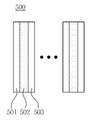
도 3은 도 1의 이방성 도전입자의 일면을 도시한 단면도이다.
도 4는 본 발명의 제2실시예에 따른 이방성 도전입자의 일면을 도시한 단면도이다.
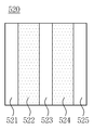
도 5는 본 발명에 따른 이방성 도전입자의 일면을 도시한 단면도이다.
도 6은 본 발명에 따른 이방성 도전입자를 포함한 이방성 도전재료를 도시한 단면도이다.
도 7은 도 6의 이방성 도전재료에 의하여 전기적으로 접속된 회로 접속 구조체를 도시한 개략도이다.
120: 전극
140: 배선
200: 구동칩
300: 이방성 도전재료
400: 절연성 접착성분
500, 510, 520: 이방성 도전입자
501, 503, 511, 513, 521, 523, 525: 절연층
502, 512, 522, 524: 도전층
Claims (11)
- 제1절연층;
상기 제1절연층상에 배치된 제1도전층; 및
상기 제1도전층상에 배치된 제2절연층;을 포함하는 이방성 도전입자. - 제1항에 있어서, 상기 도전입자는 육면체, 다면체 및 구체 중 하나인 이방성 도전입자.
- 제1항에 있어서,
상기 제2절연층상에 배치된 제2도전층; 및
상기 제2도전층상에 배치된 제3절연층;을 더 포함하는 이방성 도전입자. - 제1항에 있어서, 상기 절연층과 도전층은 교번하여 배치되며, 상기 절연층은 최상위층 및 최하위층에 배치된 이방성 도전입자.
- 제1항에 있어서, 상기 절연층 및 도전층은 10 ㎛이하의 폭을 갖는 이방성 도전입자.
- 제1항에 있어서, 상기 도전층은 Sn-Ag계 합금, Sn-Cu계 합금, Sn-Bi계 합금 또는 Sn-Zn계 합금으로 이루어진 군에서 선택되는 합금 재료를 포함하는 이방성 도전입자.
- 제1항에 있어서, 상기 Sn-Ag계 합금, Sn-Cu계 합금, Sn-Bi계 합금 및 Sn-Zn계 합금은 각각 Sn과 Ag, Sn과 Cu, Sn과 Bi, Sn과 Zn 외에 Ni, Cr, Fe, Co, Ge, P 및 Ga로 이루어진 군에서 선택되는 금속 재료를 더 포함하는 이방성 도전입자.
- 제1항에 있어서, 상기 절연층은 폴리에틸렌 및 그 공중합체, 폴리스티렌 및 그 공중합체, 폴리메틸메타크릴레이트 및 그 공중합체, 폴리비닐클로라이드 및 그 공중합체, 폴리카보네이트 및 그 공중합체, 폴리프로필렌 및 그 공중합체, 아크릴산에스테르계 고무, 폴리비닐아세탈, 폴리비닐부티랄, 아크릴로니트릴-부타디엔 공중합체, 페녹시 수지, 열가소성 에폭시 수지 및 폴리우레탄으로 이루어진 군에서 선택되는 절연성 수지를 포함하는 이방성 도전입자.
- 절연성 접착성분; 및
상기 절연성 접착성분에 분산되는 제1항 내지 제7항 중 어느 한 항에 따른 이방성 도전입자;를 포함하는 이방성 도전재료. - 제9항에 있어서, 상기 절연성 접착성분은 아세트산비닐계 수지, 염화비닐계 수지, 아크릴계 수지, 스티렌계 수지, 폴리올레핀계 수지, 에틸렌-아세트산 비닐 공중합체, 폴리아미드계 수지, 에폭시계 수지, 우레탄계 수지, 아크릴계 수지, 폴리이미드계 수지, 불포화 폴리에스테르계 수지, 스티렌-부타디엔-스티렌 블록 공중합체, 스티렌-이소프렌-스티렌 블록 공중합체, 스티렌-부타디엔 공중합 고무, 클로로프렌 고무 및 아크릴로니트릴-스티렌 블록 공중합 고무로 이루어진 군에서 선택되는 이방성 도전재료.
- 제9항에 있어서, 이방성 도전필름, 이방성 도전시트, 이방성 도전 점접착제, 이방성 도전 잉크 및 이방성 도전 페이스트로 이루어진 군에서 선택되는 이방성 도전재료.
Priority Applications (2)
| Application Number | Priority Date | Filing Date | Title |
|---|---|---|---|
| KR1020140141883A KR20160046977A (ko) | 2014-10-20 | 2014-10-20 | 이방성 도전입자 |
| US14/733,281 US9607727B2 (en) | 2014-10-20 | 2015-06-08 | Anisotropic electroconductive particles |
Applications Claiming Priority (1)
| Application Number | Priority Date | Filing Date | Title |
|---|---|---|---|
| KR1020140141883A KR20160046977A (ko) | 2014-10-20 | 2014-10-20 | 이방성 도전입자 |
Publications (1)
| Publication Number | Publication Date |
|---|---|
| KR20160046977A true KR20160046977A (ko) | 2016-05-02 |
Family
ID=55749571
Family Applications (1)
| Application Number | Title | Priority Date | Filing Date |
|---|---|---|---|
| KR1020140141883A Ceased KR20160046977A (ko) | 2014-10-20 | 2014-10-20 | 이방성 도전입자 |
Country Status (2)
| Country | Link |
|---|---|
| US (1) | US9607727B2 (ko) |
| KR (1) | KR20160046977A (ko) |
Families Citing this family (2)
| Publication number | Priority date | Publication date | Assignee | Title |
|---|---|---|---|---|
| KR20210019323A (ko) * | 2019-08-12 | 2021-02-22 | 삼성전자주식회사 | 마이크로 엘이디 디스플레이 및 이의 제작 방법 |
| CN111048499B (zh) * | 2019-12-16 | 2022-05-13 | 业成科技(成都)有限公司 | 微发光二极管显示面板及其制备方法 |
Family Cites Families (26)
| Publication number | Priority date | Publication date | Assignee | Title |
|---|---|---|---|---|
| US4778950A (en) * | 1985-07-22 | 1988-10-18 | Digital Equipment Corporation | Anisotropic elastomeric interconnecting system |
| JPH04332404A (ja) * | 1991-05-07 | 1992-11-19 | Nec Corp | 異方性導電材料及びこれを用いた集積回路素子の接続方法 |
| JPH08102218A (ja) * | 1994-09-30 | 1996-04-16 | Nec Corp | 異方性導電フィルム |
| KR100558639B1 (ko) * | 1997-02-27 | 2006-06-28 | 세이코 엡슨 가부시키가이샤 | 접착제,액정장치,액정장치의제조방법및전자기기 |
| JP3328157B2 (ja) * | 1997-03-06 | 2002-09-24 | シャープ株式会社 | 液晶表示装置 |
| JP3678547B2 (ja) * | 1997-07-24 | 2005-08-03 | ソニーケミカル株式会社 | 多層異方導電性接着剤およびその製造方法 |
| JP3372511B2 (ja) * | 1999-08-09 | 2003-02-04 | ソニーケミカル株式会社 | 半導体素子の実装方法及び実装装置 |
| JP2002032031A (ja) * | 2000-05-12 | 2002-01-31 | Seiko Epson Corp | 電気光学装置の製造方法、端子の接続方法、電気光学装置および電子機器 |
| TW531868B (en) * | 2001-08-21 | 2003-05-11 | Au Optronics Corp | Soldering type anisotropic conductive film |
| JP3910527B2 (ja) * | 2002-03-13 | 2007-04-25 | シャープ株式会社 | 液晶表示装置およびその製造方法 |
| JP2004095269A (ja) | 2002-08-30 | 2004-03-25 | Idemitsu Kosan Co Ltd | 異方導電粒子及び異方導電性接着剤 |
| KR100621463B1 (ko) * | 2003-11-06 | 2006-09-13 | 제일모직주식회사 | 절연 전도성 미립자 및 이를 함유하는 이방 전도성 필름 |
| US20080160309A1 (en) * | 2005-02-09 | 2008-07-03 | Takashi Kubota | Electrically Conductive Fine Particles, Anisotropic Electrically Conductive Material, and Electrically Conductive Connection Method |
| JP2006237484A (ja) | 2005-02-28 | 2006-09-07 | Optrex Corp | 半導体チップ,同半導体チップの製造方法および表示パネル |
| JP4591330B2 (ja) * | 2005-11-25 | 2010-12-01 | パナソニック株式会社 | 電子部品接続構造および電子部品接続方法 |
| KR20080088082A (ko) | 2007-03-28 | 2008-10-02 | 주식회사 엘지화학 | 이방성 도전접속재료용 도전성입자 및 이를 포함하는이방성 도전접속재료 |
| CN102090154B (zh) * | 2008-07-11 | 2014-11-05 | 迪睿合电子材料有限公司 | 各向异性导电薄膜 |
| KR101261184B1 (ko) * | 2009-07-01 | 2013-05-09 | 히타치가세이가부시끼가이샤 | 피복 도전 입자 및 그의 제조 방법 |
| US9102851B2 (en) * | 2011-09-15 | 2015-08-11 | Trillion Science, Inc. | Microcavity carrier belt and method of manufacture |
| JP6245792B2 (ja) * | 2012-03-29 | 2017-12-13 | デクセリアルズ株式会社 | 導電性粒子、回路接続材料、実装体、及び実装体の製造方法 |
| US8987923B2 (en) * | 2012-07-31 | 2015-03-24 | Taiwan Semiconductor Manufacturing Company Limited | Semiconductor seal ring |
| JP6066643B2 (ja) * | 2012-09-24 | 2017-01-25 | デクセリアルズ株式会社 | 異方性導電接着剤 |
| JP5985414B2 (ja) * | 2013-02-19 | 2016-09-06 | デクセリアルズ株式会社 | 異方性導電接着剤、発光装置及び異方性導電接着剤の製造方法 |
| US8987918B2 (en) * | 2013-03-14 | 2015-03-24 | Intel Corporation | Interconnect structures with polymer core |
| CN105359342B (zh) * | 2013-07-31 | 2018-02-23 | 迪睿合株式会社 | 各向异性导电膜及其制造方法 |
| US20150187453A1 (en) * | 2013-12-26 | 2015-07-02 | Hon Hai Precision Industry Co., Ltd. | Anisotropic conductive film and method for manufacturing the same |
-
2014
- 2014-10-20 KR KR1020140141883A patent/KR20160046977A/ko not_active Ceased
-
2015
- 2015-06-08 US US14/733,281 patent/US9607727B2/en not_active Expired - Fee Related
Also Published As
| Publication number | Publication date |
|---|---|
| US9607727B2 (en) | 2017-03-28 |
| US20160111181A1 (en) | 2016-04-21 |
Similar Documents
| Publication | Publication Date | Title |
|---|---|---|
| KR102103792B1 (ko) | 회로 기판의 접속 구조 | |
| US10986726B2 (en) | Flexible circuit board for all-in-one chip on film, chip package including same, and electronic device including same | |
| KR102430863B1 (ko) | 올인원 칩 온 필름용 연성 회로기판 및 이를 포함하는 칩 패키지, 및 이를 포함하는 전자 디바이스 | |
| TWI699147B (zh) | 軟性電路板及包括其的電子裝置 | |
| US9478326B2 (en) | Electroconductive microparticles, anisotropic electroconductive material, and electroconductive connection structure | |
| JP4513024B2 (ja) | 多層異方性導電フィルム | |
| DE102017129541B4 (de) | Elektronische Vorrichtung und Anzeigevorrichtung damit | |
| US9019714B2 (en) | Circuit component and method of making the same | |
| KR101396433B1 (ko) | 연성 회로 기판, 이를 포함한 반도체 패키지 및 디스플레이 장치 | |
| JP6216877B2 (ja) | 軟性印刷回路基板の構造体 | |
| KR20160046977A (ko) | 이방성 도전입자 | |
| WO2023106055A1 (ja) | 伸縮性デバイス | |
| CN110619817A (zh) | 异方性导电胶、显示面板及基板的绑定方法 | |
| KR102123813B1 (ko) | 연성 회로 기판 및 그 제조 방법 | |
| KR101040737B1 (ko) | 연성 회로 기판, 패키지, 및 평판 표시 장치 | |
| KR101588927B1 (ko) | 연성인쇄회로기판의 구조체 | |
| CN105409026B (zh) | 柔性印刷电路板结构件 | |
| KR102758192B1 (ko) | 접착제 조성물 | |
| US20090167735A1 (en) | Flexible film and display device comprising the same | |
| JP5068953B2 (ja) | コネクターを含むプラズマディスプレイ装置 | |
| KR101588928B1 (ko) | 유기 발광 소자 | |
| KR102883519B1 (ko) | 패키지 기판 및 이의 제조 방법 | |
| KR20090106777A (ko) | 도전성 입자가 부착된 전극을 구비한 연성회로기판 및테이프 캐리어 패키지 | |
| GB2559272A (en) | Electronic device and display device including the same | |
| KR101588498B1 (ko) | 연성인쇄회로기판의 구조체의 제조방법 |
Legal Events
| Date | Code | Title | Description |
|---|---|---|---|
| PA0109 | Patent application |
Patent event code: PA01091R01D Comment text: Patent Application Patent event date: 20141020 |
|
| PG1501 | Laying open of application | ||
| A201 | Request for examination | ||
| PA0201 | Request for examination |
Patent event code: PA02012R01D Patent event date: 20191015 Comment text: Request for Examination of Application Patent event code: PA02011R01I Patent event date: 20141020 Comment text: Patent Application |
|
| E902 | Notification of reason for refusal | ||
| PE0902 | Notice of grounds for rejection |
Comment text: Notification of reason for refusal Patent event date: 20210324 Patent event code: PE09021S01D |
|
| E601 | Decision to refuse application | ||
| PE0601 | Decision on rejection of patent |
Patent event date: 20210617 Comment text: Decision to Refuse Application Patent event code: PE06012S01D Patent event date: 20210324 Comment text: Notification of reason for refusal Patent event code: PE06011S01I |