KR20160050195A - 액정표시장치 및 그의 제조방법 - Google Patents
액정표시장치 및 그의 제조방법 Download PDFInfo
- Publication number
- KR20160050195A KR20160050195A KR1020140147700A KR20140147700A KR20160050195A KR 20160050195 A KR20160050195 A KR 20160050195A KR 1020140147700 A KR1020140147700 A KR 1020140147700A KR 20140147700 A KR20140147700 A KR 20140147700A KR 20160050195 A KR20160050195 A KR 20160050195A
- Authority
- KR
- South Korea
- Prior art keywords
- reflective
- reflection
- layer
- pattern
- color filter
- Prior art date
- Legal status (The legal status is an assumption and is not a legal conclusion. Google has not performed a legal analysis and makes no representation as to the accuracy of the status listed.)
- Ceased
Links
Images






Classifications
-
- G—PHYSICS
- G02—OPTICS
- G02F—OPTICAL DEVICES OR ARRANGEMENTS FOR THE CONTROL OF LIGHT BY MODIFICATION OF THE OPTICAL PROPERTIES OF THE MEDIA OF THE ELEMENTS INVOLVED THEREIN; NON-LINEAR OPTICS; FREQUENCY-CHANGING OF LIGHT; OPTICAL LOGIC ELEMENTS; OPTICAL ANALOGUE/DIGITAL CONVERTERS
- G02F1/00—Devices or arrangements for the control of the intensity, colour, phase, polarisation or direction of light arriving from an independent light source, e.g. switching, gating or modulating; Non-linear optics
- G02F1/01—Devices or arrangements for the control of the intensity, colour, phase, polarisation or direction of light arriving from an independent light source, e.g. switching, gating or modulating; Non-linear optics for the control of the intensity, phase, polarisation or colour
- G02F1/13—Devices or arrangements for the control of the intensity, colour, phase, polarisation or direction of light arriving from an independent light source, e.g. switching, gating or modulating; Non-linear optics for the control of the intensity, phase, polarisation or colour based on liquid crystals, e.g. single liquid crystal display cells
- G02F1/133—Constructional arrangements; Operation of liquid crystal cells; Circuit arrangements
- G02F1/1333—Constructional arrangements; Manufacturing methods
- G02F1/1335—Structural association of cells with optical devices, e.g. polarisers or reflectors
- G02F1/133509—Filters, e.g. light shielding masks
- G02F1/133514—Colour filters
-
- G—PHYSICS
- G02—OPTICS
- G02B—OPTICAL ELEMENTS, SYSTEMS OR APPARATUS
- G02B5/00—Optical elements other than lenses
- G02B5/20—Filters
- G02B5/201—Filters in the form of arrays
-
- G—PHYSICS
- G02—OPTICS
- G02F—OPTICAL DEVICES OR ARRANGEMENTS FOR THE CONTROL OF LIGHT BY MODIFICATION OF THE OPTICAL PROPERTIES OF THE MEDIA OF THE ELEMENTS INVOLVED THEREIN; NON-LINEAR OPTICS; FREQUENCY-CHANGING OF LIGHT; OPTICAL LOGIC ELEMENTS; OPTICAL ANALOGUE/DIGITAL CONVERTERS
- G02F1/00—Devices or arrangements for the control of the intensity, colour, phase, polarisation or direction of light arriving from an independent light source, e.g. switching, gating or modulating; Non-linear optics
- G02F1/01—Devices or arrangements for the control of the intensity, colour, phase, polarisation or direction of light arriving from an independent light source, e.g. switching, gating or modulating; Non-linear optics for the control of the intensity, phase, polarisation or colour
- G02F1/13—Devices or arrangements for the control of the intensity, colour, phase, polarisation or direction of light arriving from an independent light source, e.g. switching, gating or modulating; Non-linear optics for the control of the intensity, phase, polarisation or colour based on liquid crystals, e.g. single liquid crystal display cells
- G02F1/133—Constructional arrangements; Operation of liquid crystal cells; Circuit arrangements
- G02F1/1333—Constructional arrangements; Manufacturing methods
- G02F1/1335—Structural association of cells with optical devices, e.g. polarisers or reflectors
- G02F1/133509—Filters, e.g. light shielding masks
- G02F1/133514—Colour filters
- G02F1/133516—Methods for their manufacture, e.g. printing, electro-deposition or photolithography
-
- G—PHYSICS
- G02—OPTICS
- G02F—OPTICAL DEVICES OR ARRANGEMENTS FOR THE CONTROL OF LIGHT BY MODIFICATION OF THE OPTICAL PROPERTIES OF THE MEDIA OF THE ELEMENTS INVOLVED THEREIN; NON-LINEAR OPTICS; FREQUENCY-CHANGING OF LIGHT; OPTICAL LOGIC ELEMENTS; OPTICAL ANALOGUE/DIGITAL CONVERTERS
- G02F1/00—Devices or arrangements for the control of the intensity, colour, phase, polarisation or direction of light arriving from an independent light source, e.g. switching, gating or modulating; Non-linear optics
- G02F1/01—Devices or arrangements for the control of the intensity, colour, phase, polarisation or direction of light arriving from an independent light source, e.g. switching, gating or modulating; Non-linear optics for the control of the intensity, phase, polarisation or colour
- G02F1/13—Devices or arrangements for the control of the intensity, colour, phase, polarisation or direction of light arriving from an independent light source, e.g. switching, gating or modulating; Non-linear optics for the control of the intensity, phase, polarisation or colour based on liquid crystals, e.g. single liquid crystal display cells
- G02F1/133—Constructional arrangements; Operation of liquid crystal cells; Circuit arrangements
- G02F1/1333—Constructional arrangements; Manufacturing methods
- G02F1/1335—Structural association of cells with optical devices, e.g. polarisers or reflectors
- G02F1/133553—Reflecting elements
-
- G—PHYSICS
- G02—OPTICS
- G02F—OPTICAL DEVICES OR ARRANGEMENTS FOR THE CONTROL OF LIGHT BY MODIFICATION OF THE OPTICAL PROPERTIES OF THE MEDIA OF THE ELEMENTS INVOLVED THEREIN; NON-LINEAR OPTICS; FREQUENCY-CHANGING OF LIGHT; OPTICAL LOGIC ELEMENTS; OPTICAL ANALOGUE/DIGITAL CONVERTERS
- G02F1/00—Devices or arrangements for the control of the intensity, colour, phase, polarisation or direction of light arriving from an independent light source, e.g. switching, gating or modulating; Non-linear optics
- G02F1/01—Devices or arrangements for the control of the intensity, colour, phase, polarisation or direction of light arriving from an independent light source, e.g. switching, gating or modulating; Non-linear optics for the control of the intensity, phase, polarisation or colour
- G02F1/13—Devices or arrangements for the control of the intensity, colour, phase, polarisation or direction of light arriving from an independent light source, e.g. switching, gating or modulating; Non-linear optics for the control of the intensity, phase, polarisation or colour based on liquid crystals, e.g. single liquid crystal display cells
- G02F1/133—Constructional arrangements; Operation of liquid crystal cells; Circuit arrangements
- G02F1/1333—Constructional arrangements; Manufacturing methods
- G02F1/1343—Electrodes
- G02F1/134309—Electrodes characterised by their geometrical arrangement
-
- G—PHYSICS
- G02—OPTICS
- G02F—OPTICAL DEVICES OR ARRANGEMENTS FOR THE CONTROL OF LIGHT BY MODIFICATION OF THE OPTICAL PROPERTIES OF THE MEDIA OF THE ELEMENTS INVOLVED THEREIN; NON-LINEAR OPTICS; FREQUENCY-CHANGING OF LIGHT; OPTICAL LOGIC ELEMENTS; OPTICAL ANALOGUE/DIGITAL CONVERTERS
- G02F1/00—Devices or arrangements for the control of the intensity, colour, phase, polarisation or direction of light arriving from an independent light source, e.g. switching, gating or modulating; Non-linear optics
- G02F1/01—Devices or arrangements for the control of the intensity, colour, phase, polarisation or direction of light arriving from an independent light source, e.g. switching, gating or modulating; Non-linear optics for the control of the intensity, phase, polarisation or colour
- G02F1/13—Devices or arrangements for the control of the intensity, colour, phase, polarisation or direction of light arriving from an independent light source, e.g. switching, gating or modulating; Non-linear optics for the control of the intensity, phase, polarisation or colour based on liquid crystals, e.g. single liquid crystal display cells
- G02F1/133—Constructional arrangements; Operation of liquid crystal cells; Circuit arrangements
- G02F1/1333—Constructional arrangements; Manufacturing methods
- G02F1/1343—Electrodes
- G02F1/13439—Electrodes characterised by their electrical, optical, physical properties; materials therefor; method of making
-
- G—PHYSICS
- G02—OPTICS
- G02F—OPTICAL DEVICES OR ARRANGEMENTS FOR THE CONTROL OF LIGHT BY MODIFICATION OF THE OPTICAL PROPERTIES OF THE MEDIA OF THE ELEMENTS INVOLVED THEREIN; NON-LINEAR OPTICS; FREQUENCY-CHANGING OF LIGHT; OPTICAL LOGIC ELEMENTS; OPTICAL ANALOGUE/DIGITAL CONVERTERS
- G02F1/00—Devices or arrangements for the control of the intensity, colour, phase, polarisation or direction of light arriving from an independent light source, e.g. switching, gating or modulating; Non-linear optics
- G02F1/01—Devices or arrangements for the control of the intensity, colour, phase, polarisation or direction of light arriving from an independent light source, e.g. switching, gating or modulating; Non-linear optics for the control of the intensity, phase, polarisation or colour
- G02F1/13—Devices or arrangements for the control of the intensity, colour, phase, polarisation or direction of light arriving from an independent light source, e.g. switching, gating or modulating; Non-linear optics for the control of the intensity, phase, polarisation or colour based on liquid crystals, e.g. single liquid crystal display cells
- G02F1/133—Constructional arrangements; Operation of liquid crystal cells; Circuit arrangements
- G02F1/1333—Constructional arrangements; Manufacturing methods
- G02F1/1335—Structural association of cells with optical devices, e.g. polarisers or reflectors
- G02F1/133553—Reflecting elements
- G02F1/133555—Transflectors
-
- G—PHYSICS
- G02—OPTICS
- G02F—OPTICAL DEVICES OR ARRANGEMENTS FOR THE CONTROL OF LIGHT BY MODIFICATION OF THE OPTICAL PROPERTIES OF THE MEDIA OF THE ELEMENTS INVOLVED THEREIN; NON-LINEAR OPTICS; FREQUENCY-CHANGING OF LIGHT; OPTICAL LOGIC ELEMENTS; OPTICAL ANALOGUE/DIGITAL CONVERTERS
- G02F1/00—Devices or arrangements for the control of the intensity, colour, phase, polarisation or direction of light arriving from an independent light source, e.g. switching, gating or modulating; Non-linear optics
- G02F1/01—Devices or arrangements for the control of the intensity, colour, phase, polarisation or direction of light arriving from an independent light source, e.g. switching, gating or modulating; Non-linear optics for the control of the intensity, phase, polarisation or colour
- G02F1/13—Devices or arrangements for the control of the intensity, colour, phase, polarisation or direction of light arriving from an independent light source, e.g. switching, gating or modulating; Non-linear optics for the control of the intensity, phase, polarisation or colour based on liquid crystals, e.g. single liquid crystal display cells
- G02F1/133—Constructional arrangements; Operation of liquid crystal cells; Circuit arrangements
- G02F1/136—Liquid crystal cells structurally associated with a semi-conducting layer or substrate, e.g. cells forming part of an integrated circuit
- G02F1/1362—Active matrix addressed cells
- G02F1/136222—Colour filters incorporated in the active matrix substrate
Landscapes
- Physics & Mathematics (AREA)
- Nonlinear Science (AREA)
- General Physics & Mathematics (AREA)
- Optics & Photonics (AREA)
- Mathematical Physics (AREA)
- Chemical & Material Sciences (AREA)
- Crystallography & Structural Chemistry (AREA)
- Geometry (AREA)
- Engineering & Computer Science (AREA)
- Manufacturing & Machinery (AREA)
- Liquid Crystal (AREA)
Abstract
Description
도 2는 도 1의 Ⅰ ~ Ⅰ'을 따라 절단한 단면도이다.
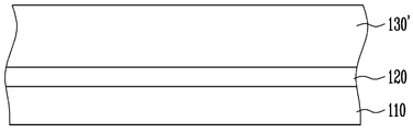
도 3a 내지 도 3h는 도 2의 반사부의 제조 공정을 순차적으로 나타낸 단면도들이다.
도 4는 도 2의 투명층 및 컬러필터의 다른 실시예를 나타낸 단면도이다.
도 5는 본 발명의 제2 실시예에 따른 액정표시장치의 화소 영역을 나타낸 도면이다.
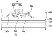
도 6은 도 5의 Ⅱ ~ Ⅱ'을 따라 절단한 단면도이다.
도 7은 도 6의 투명층 및 컬러필터의 다른 실시예를 나타낸 단면도이다.
도 8은 본 발명의 제3 실시예에 따른 액정표시장치의 화소 영역을 나타낸 도면이다.
도 9는 도 8의 Ⅲ ~ Ⅲ'을 따라 절단한 단면도이다.
도 10은 도 9의 투명층 및 컬러필터의 다른 실시예를 나타낸 단면도이다.
도 11은 본 발명의 제4 실시예에 따른 액정표시장치의 화소 영역을 나타낸 도면이다.
도 12는 도 11의 Ⅳ ~ Ⅳ'을 따라 절단한 단면도이다.
120/320/320/720: 어레이층 130/330/550/750: 유기층
140/340/540/740: 반사 전극 150/250/350/450/550/650/750: 투명층
160/260/360/460/560/660/760: 컬러필터층
Claims (13)
- 투과 영역과 반사 영역을 구비한 절연 기판;
상기 절연 기판 상에 위치하며 상기 반사 영역에서 삼각 패턴을 갖는 유기층;
상기 반사 영역에서 상기 유기층의 삼각 패턴에 대응되는 반사 패턴을 구비한 반사 전극;
상기 반사 전극 상에 위치하며 상기 반사 패턴의 일부 영역을 노출시키는 개구부를 구비한 컬러필터층; 및
상기 컬러필터층의 개구부 내부에 형성되는 투명층;을 포함한 액정표시장치. - 제1 항에 있어서,
상기 반사 패턴은 사각뿔 형상을 갖는 것을 특징으로 하는 액정표시장치. - 제1 항에 있어서,
상기 반사 전극은 상기 반사 패턴을 5개로 묶은 형태로 상기 반사 영역에서 적어도 하나 이상 구비되는 것을 특징으로 하는 액정표시장치. - 제3 항에 있어서,
상기 컬러필터층의 개구부는 5개의 반사 패턴 중 가운데 반사 패턴을 노출시키는 것을 특징으로 하는 액정표시장치. - 제4 항에 있어서,
상기 투명층은 상기 가운데 반사 패턴에 대응되는 제1 투명층 및 상기 가운데 반사 패턴을 둘러싸는 4개의 반사 패턴의 일부에 대응되는 제2 투명층을 더 포함하는 것을 특징으로 하는 액정표시장치. - 제3 항에 있어서,
상기 반사 전극의 5개의 반사 패턴은 동일한 폭을 갖는 것을 특징으로 하는 액정표시장치. - 제5 항에 있어서,
상기 가운데 반사 패턴의 폭과 상기 가운데 반사 패턴을 둘러싸는 4개의 반사 패턴의 폭은 서로 상이한 것을 특징으로 하는 액정표시장치. - 제1 항에 있어서,
상기 투명층은 투명한 절연막을 포함하는 것을 특징으로 하는 액정표시장치. - 투과 영역과 반사 영역을 구비한 절연 기판을 포함하는 액정표시장치의 제조방법에 있어서,
상기 절연 기판의 반사 영역 상에 삼각 패턴을 갖는 유기층을 형성하는 단계;
상기 유기층 상에 상기 유기층의 삼각 패턴에 대응되는 반사 패턴을 포함하는 반사 전극을 형성하는 단계;
상기 반사 전극의 일부 반사 패턴 상에 투명층을 형성하는 단계; 및
상기 절연 기판 상에 상기 투명층에 대응되는 개구부를 포함하는 컬러필터층을 형성하는 단계;를 포함하는 액정표시장치의 제조방법. - 제9 항에 있어서,
상기 반사 패턴은 사각뿔 형상을 갖는 것을 특징으로 하는 액정표시장치의 제조방법. - 제9 항에 있어서,
상기 반사 전극은 상기 반사 패턴을 5개로 묶는 형태로 상기 반사 영역에서 적어도 하나 이상으로 구비되는 것을 특징으로 하는 액정표시장치의 제조방법. - 제11 항에 있어서,
상기 컬러필터층의 개구부는 상기 5개의 반사 패턴 중 가운데 반사 패턴을 노출시키는 것을 특징으로 하는 액정표시장치의 제조방법. - 제12 항에 있어서,
상기 투명층은 상기 가운데 반사 패턴에 대응되는 제1 투명층 및 상기 가운데 반사 패턴을 둘러싸는 4개의 반사 패턴의 일부에 대응되는 제2 투명층을 더 포함하는 것을 특징으로 하는 액정표시장치의 제조방법.
Priority Applications (2)
| Application Number | Priority Date | Filing Date | Title |
|---|---|---|---|
| KR1020140147700A KR20160050195A (ko) | 2014-10-28 | 2014-10-28 | 액정표시장치 및 그의 제조방법 |
| US14/745,059 US9664944B2 (en) | 2014-10-28 | 2015-06-19 | Liquid crystal display device and method of fabricating the same |
Applications Claiming Priority (1)
| Application Number | Priority Date | Filing Date | Title |
|---|---|---|---|
| KR1020140147700A KR20160050195A (ko) | 2014-10-28 | 2014-10-28 | 액정표시장치 및 그의 제조방법 |
Publications (1)
| Publication Number | Publication Date |
|---|---|
| KR20160050195A true KR20160050195A (ko) | 2016-05-11 |
Family
ID=55791891
Family Applications (1)
| Application Number | Title | Priority Date | Filing Date |
|---|---|---|---|
| KR1020140147700A Ceased KR20160050195A (ko) | 2014-10-28 | 2014-10-28 | 액정표시장치 및 그의 제조방법 |
Country Status (2)
| Country | Link |
|---|---|
| US (1) | US9664944B2 (ko) |
| KR (1) | KR20160050195A (ko) |
Families Citing this family (1)
| Publication number | Priority date | Publication date | Assignee | Title |
|---|---|---|---|---|
| JP2019082594A (ja) * | 2017-10-31 | 2019-05-30 | ソニー株式会社 | 表示装置 |
Family Cites Families (13)
| Publication number | Priority date | Publication date | Assignee | Title |
|---|---|---|---|---|
| JP3834458B2 (ja) | 2000-07-03 | 2006-10-18 | シャープ株式会社 | 液晶表示装置 |
| KR20010067948A (ko) | 2001-04-10 | 2001-07-13 | 김현주 | 이동통신 단말기의 액정표시소자용 백라이트 장치 |
| KR20010069938A (ko) | 2001-05-21 | 2001-07-25 | 김현주 | 개인휴대통신 단말기의 액정표시소자용 프런트라이트 장치 |
| JP4822486B2 (ja) | 2001-09-26 | 2011-11-24 | Nltテクノロジー株式会社 | 半透過反射板及び半透過型液晶表示装置 |
| JP2003255323A (ja) | 2002-03-04 | 2003-09-10 | Matsushita Electric Ind Co Ltd | 液晶表示装置 |
| JP2004179116A (ja) | 2002-11-29 | 2004-06-24 | Alps Electric Co Ltd | 背面照明装置及び液晶表示装置 |
| JP2005321693A (ja) | 2004-05-11 | 2005-11-17 | Hitachi Displays Ltd | 液晶表示装置 |
| JP2006171207A (ja) | 2004-12-14 | 2006-06-29 | Casio Comput Co Ltd | 光源ユニット及びプロジェクタ装置 |
| KR20060079695A (ko) | 2005-01-03 | 2006-07-06 | 삼성전자주식회사 | 액정 표시 장치 |
| KR20060080271A (ko) | 2005-01-04 | 2006-07-10 | 삼성전자주식회사 | 표시 기판 및 이의 제조 방법 |
| JP4746933B2 (ja) * | 2005-08-01 | 2011-08-10 | Nec液晶テクノロジー株式会社 | カラー電子ペーパー表示装置 |
| US8142032B2 (en) | 2007-06-25 | 2012-03-27 | Casio Computer Co., Ltd. | Optical system unit for projecting images and including light smoothing unit formed into substantially truncated quadrangular pyramid, and projector including the same optical system |
| JP5217447B2 (ja) | 2008-01-21 | 2013-06-19 | 凸版印刷株式会社 | 光源ユニット、バックライトユニット及びディスプレイ装置 |
-
2014
- 2014-10-28 KR KR1020140147700A patent/KR20160050195A/ko not_active Ceased
-
2015
- 2015-06-19 US US14/745,059 patent/US9664944B2/en active Active
Also Published As
| Publication number | Publication date |
|---|---|
| US20160116796A1 (en) | 2016-04-28 |
| US9664944B2 (en) | 2017-05-30 |
Similar Documents
| Publication | Publication Date | Title |
|---|---|---|
| US8264778B2 (en) | Display substrate, method of manufacturing the same and electrowetting display panel having the display substrate | |
| CN103185981B (zh) | 彩色滤光阵列基板及其制备方法和显示装置 | |
| JP3928543B2 (ja) | 電機光学装置用基板及びその製造方法、電気光学装置並びに電子機器 | |
| KR20030007137A (ko) | 컬러 필터 기판 및 전기 광학 장치, 컬러 필터 기판의제조 방법 및 전기 광학 장치의 제조 방법 및 전자 기기 | |
| KR102344911B1 (ko) | 광루미네선스 장치, 이의 제조 방법 및 이를 포함하는 표시 장치 | |
| US8241935B2 (en) | Method of fabricating liquid crystal display device having concave reflector | |
| JP3844846B2 (ja) | 液晶表示装置およびその製造方法 | |
| US7123327B2 (en) | Substrate for reflective-transmissive electro-optical device having opening in base layer varying in size along a first direction | |
| CN1523436B (zh) | 半透射式液晶显示装置 | |
| KR100594664B1 (ko) | 전기 광학 장치용 기판의 제조 방법 및 전기 광학 장치의제조 방법 | |
| US20060132678A1 (en) | Color filter substrate and liquid crystal display device | |
| JP2003043239A (ja) | カラーフィルタ基板及びその製造方法並びに液晶表示装置 | |
| KR20160050195A (ko) | 액정표시장치 및 그의 제조방법 | |
| JP2000241809A (ja) | 反射型液晶表示装置 | |
| JP2006058876A (ja) | マスク、薄膜トランジスタ基板、及び薄膜トランジスタ基板の製造方法、ならびに薄膜トランジスタ基板を有する表示装置 | |
| KR100660671B1 (ko) | 전기 광학 장치용 기판 및 그 제조 방법, 전기 광학 장치및 그 제조 방법, 노광용 마스크, 및 전자기기 | |
| US20220131077A1 (en) | Mask plate, display panel and display device | |
| JP2007114770A (ja) | アレイ基板及びその製造方法並びにそれを有する液晶表示装置 | |
| KR100433594B1 (ko) | 액정표시장치 | |
| TWI852744B (zh) | 前光模組、反射式顯示裝置以及前光模組的製造方法 | |
| KR100897741B1 (ko) | 반사-투과형 액정표시장치 및 이의 제조 방법 | |
| KR20070065065A (ko) | 반투과형 액정 표시 장치의 제조 방법 | |
| KR20080026721A (ko) | 컬러필터기판 및 이를 갖는 액정표시장치 | |
| JP4512328B2 (ja) | フォトマスク、拡散反射板及びその製造方法並びにカラーフィルタ | |
| KR100995581B1 (ko) | 컬러필터기판, 이를 갖는 액정표시장치 및 이의 제조방법 |
Legal Events
| Date | Code | Title | Description |
|---|---|---|---|
| PA0109 | Patent application |
Patent event code: PA01091R01D Comment text: Patent Application Patent event date: 20141028 |
|
| PG1501 | Laying open of application | ||
| A201 | Request for examination | ||
| PA0201 | Request for examination |
Patent event code: PA02012R01D Patent event date: 20190927 Comment text: Request for Examination of Application Patent event code: PA02011R01I Patent event date: 20141028 Comment text: Patent Application |
|
| E902 | Notification of reason for refusal | ||
| PE0902 | Notice of grounds for rejection |
Comment text: Notification of reason for refusal Patent event date: 20200831 Patent event code: PE09021S01D |
|
| E601 | Decision to refuse application | ||
| PE0601 | Decision on rejection of patent |
Patent event date: 20201109 Comment text: Decision to Refuse Application Patent event code: PE06012S01D Patent event date: 20200831 Comment text: Notification of reason for refusal Patent event code: PE06011S01I |