KR20160052576A - 액체 유리의 응용 - Google Patents
액체 유리의 응용 Download PDFInfo
- Publication number
- KR20160052576A KR20160052576A KR1020167006860A KR20167006860A KR20160052576A KR 20160052576 A KR20160052576 A KR 20160052576A KR 1020167006860 A KR1020167006860 A KR 1020167006860A KR 20167006860 A KR20167006860 A KR 20167006860A KR 20160052576 A KR20160052576 A KR 20160052576A
- Authority
- KR
- South Korea
- Prior art keywords
- glass layer
- thickness
- layer
- glass
- conductive posts
- Prior art date
- Legal status (The legal status is an assumption and is not a legal conclusion. Google has not performed a legal analysis and makes no representation as to the accuracy of the status listed.)
- Ceased
Links
Images












Classifications
-
- H—ELECTRICITY
- H05—ELECTRIC TECHNIQUES NOT OTHERWISE PROVIDED FOR
- H05K—PRINTED CIRCUITS; CASINGS OR CONSTRUCTIONAL DETAILS OF ELECTRIC APPARATUS; MANUFACTURE OF ASSEMBLAGES OF ELECTRICAL COMPONENTS
- H05K1/00—Printed circuits
- H05K1/02—Details
- H05K1/03—Use of materials for the substrate
- H05K1/0306—Inorganic insulating substrates, e.g. ceramic, glass
-
- H—ELECTRICITY
- H10—SEMICONDUCTOR DEVICES; ELECTRIC SOLID-STATE DEVICES NOT OTHERWISE PROVIDED FOR
- H10D—INORGANIC ELECTRIC SEMICONDUCTOR DEVICES
- H10D86/00—Integrated devices formed in or on insulating or conducting substrates, e.g. formed in silicon-on-insulator [SOI] substrates or on stainless steel or glass substrates
- H10D86/01—Manufacture or treatment
-
- H01L21/84—
-
- C—CHEMISTRY; METALLURGY
- C03—GLASS; MINERAL OR SLAG WOOL
- C03B—MANUFACTURE, SHAPING, OR SUPPLEMENTARY PROCESSES
- C03B19/00—Other methods of shaping glass
- C03B19/12—Other methods of shaping glass by liquid-phase reaction processes
-
- C—CHEMISTRY; METALLURGY
- C03—GLASS; MINERAL OR SLAG WOOL
- C03B—MANUFACTURE, SHAPING, OR SUPPLEMENTARY PROCESSES
- C03B23/00—Re-forming shaped glass
- C03B23/02—Re-forming glass sheets
-
- H01L21/02422—
-
- H01L21/08—
-
- H—ELECTRICITY
- H05—ELECTRIC TECHNIQUES NOT OTHERWISE PROVIDED FOR
- H05K—PRINTED CIRCUITS; CASINGS OR CONSTRUCTIONAL DETAILS OF ELECTRIC APPARATUS; MANUFACTURE OF ASSEMBLAGES OF ELECTRICAL COMPONENTS
- H05K1/00—Printed circuits
- H05K1/02—Details
- H05K1/03—Use of materials for the substrate
- H05K1/0313—Organic insulating material
- H05K1/032—Organic insulating material consisting of one material
-
- H—ELECTRICITY
- H05—ELECTRIC TECHNIQUES NOT OTHERWISE PROVIDED FOR
- H05K—PRINTED CIRCUITS; CASINGS OR CONSTRUCTIONAL DETAILS OF ELECTRIC APPARATUS; MANUFACTURE OF ASSEMBLAGES OF ELECTRICAL COMPONENTS
- H05K3/00—Apparatus or processes for manufacturing printed circuits
- H05K3/007—Manufacture or processing of a substrate for a printed circuit board supported by a temporary or sacrificial carrier
-
- H—ELECTRICITY
- H05—ELECTRIC TECHNIQUES NOT OTHERWISE PROVIDED FOR
- H05K—PRINTED CIRCUITS; CASINGS OR CONSTRUCTIONAL DETAILS OF ELECTRIC APPARATUS; MANUFACTURE OF ASSEMBLAGES OF ELECTRICAL COMPONENTS
- H05K3/00—Apparatus or processes for manufacturing printed circuits
- H05K3/02—Apparatus or processes for manufacturing printed circuits in which the conductive material is applied to the surface of the insulating support and is thereafter removed from such areas of the surface which are not intended for current conducting or shielding
- H05K3/06—Apparatus or processes for manufacturing printed circuits in which the conductive material is applied to the surface of the insulating support and is thereafter removed from such areas of the surface which are not intended for current conducting or shielding the conductive material being removed chemically or electrolytically, e.g. by photo-etch process
- H05K3/061—Etching masks
- H05K3/064—Photoresists
-
- H—ELECTRICITY
- H05—ELECTRIC TECHNIQUES NOT OTHERWISE PROVIDED FOR
- H05K—PRINTED CIRCUITS; CASINGS OR CONSTRUCTIONAL DETAILS OF ELECTRIC APPARATUS; MANUFACTURE OF ASSEMBLAGES OF ELECTRICAL COMPONENTS
- H05K3/00—Apparatus or processes for manufacturing printed circuits
- H05K3/22—Secondary treatment of printed circuits
- H05K3/28—Applying non-metallic protective coatings
-
- H—ELECTRICITY
- H05—ELECTRIC TECHNIQUES NOT OTHERWISE PROVIDED FOR
- H05K—PRINTED CIRCUITS; CASINGS OR CONSTRUCTIONAL DETAILS OF ELECTRIC APPARATUS; MANUFACTURE OF ASSEMBLAGES OF ELECTRICAL COMPONENTS
- H05K3/00—Apparatus or processes for manufacturing printed circuits
- H05K3/40—Forming printed elements for providing electric connections to or between printed circuits
- H05K3/4038—Through-connections; Vertical interconnect access [VIA] connections
-
- H—ELECTRICITY
- H10—SEMICONDUCTOR DEVICES; ELECTRIC SOLID-STATE DEVICES NOT OTHERWISE PROVIDED FOR
- H10D—INORGANIC ELECTRIC SEMICONDUCTOR DEVICES
- H10D48/00—Individual devices not covered by groups H10D1/00 - H10D44/00
- H10D48/01—Manufacture or treatment
- H10D48/04—Manufacture or treatment of devices having bodies comprising selenium or tellurium in uncombined form
- H10D48/042—Preparation of foundation plates
-
- H—ELECTRICITY
- H10—SEMICONDUCTOR DEVICES; ELECTRIC SOLID-STATE DEVICES NOT OTHERWISE PROVIDED FOR
- H10P—GENERIC PROCESSES OR APPARATUS FOR THE MANUFACTURE OR TREATMENT OF DEVICES COVERED BY CLASS H10
- H10P14/00—Formation of materials, e.g. in the shape of layers or pillars
- H10P14/20—Formation of materials, e.g. in the shape of layers or pillars of semiconductor materials
- H10P14/29—Formation of materials, e.g. in the shape of layers or pillars of semiconductor materials characterised by the substrates
- H10P14/2901—Materials
- H10P14/2922—Materials being non-crystalline insulating materials, e.g. glass or polymers
Landscapes
- Engineering & Computer Science (AREA)
- Chemical & Material Sciences (AREA)
- Microelectronics & Electronic Packaging (AREA)
- Manufacturing & Machinery (AREA)
- Materials Engineering (AREA)
- Organic Chemistry (AREA)
- Ceramic Engineering (AREA)
- Inorganic Chemistry (AREA)
- Chemical Kinetics & Catalysis (AREA)
- Laminated Bodies (AREA)
- Printing Elements For Providing Electric Connections Between Printed Circuits (AREA)
- Manufacturing Of Printed Wiring (AREA)
- Production Of Multi-Layered Print Wiring Board (AREA)
Abstract
Description
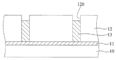
도 2a 내지 도 2c는 본 발명에 따른 회로가 내장된 기판 및 상기 기판을 제조하기 위한 방법을 나타내는 단면도들이다.
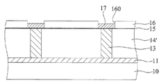
도 3a 내지 도 3d는 본 발명에 따른 회로가 내장된 기판 및 상기 기판을 제조하기 위한 방법을 나타내는 단면도들이다.
Claims (23)
- 캐리어 보드(carrier board) 상에 복수의 도전성 기둥들(conductive posts)을 형성하는단계;
상기 도전성 기둥들을 밀봉하기(encapsulate) 위해 상기 캐리어 보드 상에 액체 유리 층을 코팅하는 단계;
50 과 100℃ 사이의 열처리 온도(baking temperature)에서 열처리하는 단계;
자외선으로 조사하는 단계(irradiating); 및
상기 캐리어 보드를 제거하는 단계를 포함하며,
상기 액체 유리 층의 상부 면은 상기 도전성 기둥들의 상단과 높이가 동일한, 기판 제조 방법. - 청구항 1에 있어서, 상기 열처리 온도는 바람직하게는 70 과 95℃ 사이인 기판 제조 방법.
- 청구항 1에 있어서, 상기 열처리는 3 에서 55분이 소요되는 기판 제조 방법.
- 청구항 1에 있어서, 상기 액체 유리 층은 2 에서 25μm 의 두께를 갖는 기판 제조 방법.
- 청구항 1에 있어서, 상기 도전성 기둥들은 전기도금(electroplating) 또는 증착(deposition)에 의하여 형성되는 기판 제조 방법.
- 청구항 1에 있어서, 상기 도전성 기둥들을 형성하는 단계는,
상기 캐리어 보드 상에 복수의 개구들(openings)을 갖는 레지스트(resist) 층을 형성하는 단계;
상기 레지스트 층의 상기 개구들 내에 상기 도전성 기둥들을 형성하는 단계;
상기 레지스트 층을 제거하는 단계를 포함하는 기판 제조 방법. - 청구항 1에 있어서, 상기 도전성 기둥들의 측벽들과 상기 도전성 기둥들 부근의 상기 캐리어 보드 사이에 85 에서 90°의 기울기가 형성되는 기판 제조 방법.
- 2 에서 25μm 의 두께를 갖는 유리 베이스; 및
상기 유리 베이스의 두 표면을 관통하는 복수의 도전성 기둥들을 포함하는 기판. - 청구항 8에 있어서, 상기 도전성 기둥들의 측벽들과 상기 유리 베이스의 상기 표면들의 사이에 85 에서 95° 의 기울기가 형성되는 기판.
- 2 에서 100μm 의 두께를 갖는 폴리이미드(polyimide) 베이스; 및
상기 폴리이미드 베이스의 두 표면들을 관통하는 복수의 도전성 기둥들을 포함하는 기판. - 청구항 10에 있어서, 상기 도전성 기둥들의 측벽들과 상기 폴리이미드 베이스의 상기 표면들 사이에 85 에서 95° 의 기울기가 형성되는 기판.
- 청구항 10에 있어서, 상기 폴리이미드 베이스의 상기 두께는 2 에서 25μm 의 범위 내에 있는 기판.
- 서로 번갈아 가면서(alternatively) 적층된 적어도 하나의 회로 층 및 적어도 하나의 유리 층으로 구성된 재배치(redistribution) 층 구조를 캐리어 보드 상에 형성하는 단계; 및
상기 캐리어 보드를 제거하는 단계를 포함하며,
상기 유리 층은 액체 유리 층을 코팅하는 단계, 50 과 100℃ 사이의 열처리 온도에서 열처리하는 단계, 및 자외선으로 조사하는 단계들을 순차적으로 수행함에 따라 형성되는, 회로가 내장된 기판을 제조하는 방법. - 청구항 13에 있어서, 상기 열처리 온도는 바람직하게는 70 과 95℃ 사이인, 회로가 내장된 기판을 제조하는 방법.
- 청구항 13에 있어서, 상기 열처리는 상기 유리 층의 상기 두께에 따라 3 에서 55 분이 소요되는, 회로가 내장된 기판을 제조하는 방법.
- 청구항 13에 있어서, 상기 유리 층은 2 에서 25μm 의 두께를 갖는, 회로가 내장된 기판을 제조하는 방법.
- 서로 번갈아 가면서 적층된 적어도 하나의 회로 층 및 적어도 하나의 유리 층으로 구성된 재배치 층 구조를 포함하며, 상기 유리 층은 2 에서 25μm 의 두께를 갖는, 회로가 내장된 기판.
- 캐리어 필름 상에 액체 유리 층을 코팅하는 단계;
50 과 100℃ 사이의 열처리 온도에서 열처리하는 단계;
상기 액체 유리 층의 표면 상의 요철 패턴을 찍어 누르고(impress) 자외선을 조사하는 단계; 및
상기 캐리어 필름을 제거하는 단계를 포함하는, 유리 막(membrane) 제조 방법. - 청구항 18에 있어서, 상기 열처리 온도는 바람직하게는 70 과 95℃ 사이인, 유리 막 제조 방법.
- 청구항 18에 있어서, 상기 열처리는 상기 액체 유리 층의 상기 두께에 따라 3 에서 55분이 소요되는, 유리 막 제조 방법.
- 청구항 18에 있어서, 상기 액체 유리 층은 2 에서 25μm의 두께를 갖는, 유리 막 제조 방법.
- 청구항 18에 있어서, 상기 찍어 누르는 단계는 롤러를 사용하여 수행되는, 유리 막 제조 방법.
- 그 표면에 규칙적이거나 불규칙적인 요철 패턴을 구비하는 유리 보드를 포함하며, 상기 유리 보드는 2 에서 25μm 의 두께를 가지는, 유리 막.
Applications Claiming Priority (1)
| Application Number | Priority Date | Filing Date | Title |
|---|---|---|---|
| PCT/CN2013/083038 WO2015032062A1 (zh) | 2013-09-06 | 2013-09-06 | 液态玻璃的应用 |
Publications (1)
| Publication Number | Publication Date |
|---|---|
| KR20160052576A true KR20160052576A (ko) | 2016-05-12 |
Family
ID=52627704
Family Applications (1)
| Application Number | Title | Priority Date | Filing Date |
|---|---|---|---|
| KR1020167006860A Ceased KR20160052576A (ko) | 2013-09-06 | 2013-09-06 | 액체 유리의 응용 |
Country Status (5)
| Country | Link |
|---|---|
| US (1) | US20160205774A1 (ko) |
| JP (1) | JP2016532304A (ko) |
| KR (1) | KR20160052576A (ko) |
| CN (1) | CN105518824A (ko) |
| WO (1) | WO2015032062A1 (ko) |
Families Citing this family (2)
| Publication number | Priority date | Publication date | Assignee | Title |
|---|---|---|---|---|
| CN110088894B (zh) * | 2016-12-21 | 2023-09-12 | 株式会社村田制作所 | 电子部件内置基板的制造方法、电子部件内置基板、电子部件装置及通信模块 |
| WO2019199470A1 (en) * | 2018-04-10 | 2019-10-17 | 3D Glass Solutions, Inc. | Rf integrated power condition capacitor |
Family Cites Families (20)
| Publication number | Priority date | Publication date | Assignee | Title |
|---|---|---|---|---|
| JPH03232116A (ja) * | 1990-02-07 | 1991-10-16 | Nippon Sheet Glass Co Ltd | ガラス製磁気ディスク基板の製造方法 |
| JP4189056B2 (ja) * | 1998-05-15 | 2008-12-03 | 株式会社カネカ | 太陽電池モジュールおよびその製造方法 |
| EP1048628A1 (de) * | 1999-04-30 | 2000-11-02 | Schott Glas | Polymerbeschichtete Dünnglasfoliensubstrate |
| JP2001294489A (ja) * | 2000-04-07 | 2001-10-23 | Tokuyama Corp | 結晶化ガラスと窒化アルミニウム焼結体との接合体 |
| JP2002110717A (ja) * | 2000-10-02 | 2002-04-12 | Sanyo Electric Co Ltd | 回路装置の製造方法 |
| JP4812935B2 (ja) * | 2000-12-20 | 2011-11-09 | 学校法人日本大学 | ハードコート膜形成方法 |
| JP4748340B2 (ja) * | 2001-03-22 | 2011-08-17 | 日立化成工業株式会社 | 金属薄膜層が形成された接続用導体内蔵の両面板製造方法 |
| TW200302685A (en) * | 2002-01-23 | 2003-08-01 | Matsushita Electric Industrial Co Ltd | Circuit component built-in module and method of manufacturing the same |
| JP3524545B2 (ja) * | 2002-01-23 | 2004-05-10 | 松下電器産業株式会社 | 回路部品内蔵モジュールの製造方法 |
| EP1605739A4 (en) * | 2003-04-18 | 2009-08-19 | Ibiden Co Ltd | RIGID-FLEXIBLE CONNECTION CHART |
| WO2005027606A1 (ja) * | 2003-09-09 | 2005-03-24 | Hoya Corporation | 両面配線ガラス基板の製造方法 |
| JP2005243911A (ja) * | 2004-02-26 | 2005-09-08 | Mitsui Mining & Smelting Co Ltd | 多層積層配線板 |
| JP2005285849A (ja) * | 2004-03-26 | 2005-10-13 | North:Kk | 多層配線基板製造用層間部材とその製造方法 |
| JP4305399B2 (ja) * | 2004-06-10 | 2009-07-29 | 住友電気工業株式会社 | 多層プリント配線板の製造方法及び多層プリント配線板 |
| US7682972B2 (en) * | 2006-06-01 | 2010-03-23 | Amitec-Advanced Multilayer Interconnect Technoloiges Ltd. | Advanced multilayer coreless support structures and method for their fabrication |
| JP5117692B2 (ja) * | 2006-07-14 | 2013-01-16 | ルネサスエレクトロニクス株式会社 | 半導体装置の製造方法 |
| EP2157842B1 (en) * | 2007-05-17 | 2018-03-14 | Fujikura, Ltd. | Laminated wiring board and method for manufacturing the same |
| JP2009179518A (ja) * | 2008-01-30 | 2009-08-13 | Hoya Corp | 結晶化ガラス基板の製造方法及び両面配線基板の製造方法 |
| JP2012156403A (ja) * | 2011-01-27 | 2012-08-16 | Panasonic Corp | ガラス埋込シリコン基板およびその製造方法 |
| JP2013010651A (ja) * | 2011-06-28 | 2013-01-17 | Asahi Glass Co Ltd | インターポーザ用基板の製造方法 |
-
2013
- 2013-09-06 KR KR1020167006860A patent/KR20160052576A/ko not_active Ceased
- 2013-09-06 CN CN201380079307.9A patent/CN105518824A/zh active Pending
- 2013-09-06 WO PCT/CN2013/083038 patent/WO2015032062A1/zh not_active Ceased
- 2013-09-06 JP JP2016539380A patent/JP2016532304A/ja active Pending
- 2013-09-06 US US14/916,994 patent/US20160205774A1/en not_active Abandoned
Also Published As
| Publication number | Publication date |
|---|---|
| CN105518824A (zh) | 2016-04-20 |
| JP2016532304A (ja) | 2016-10-13 |
| WO2015032062A1 (zh) | 2015-03-12 |
| US20160205774A1 (en) | 2016-07-14 |
Similar Documents
| Publication | Publication Date | Title |
|---|---|---|
| Tian et al. | Optical rashba effect in a light‐emitting perovskite metasurface | |
| US10629744B2 (en) | Electronic device and method for fabricating the same | |
| TWI798279B (zh) | 使用保護性材料的貫穿玻璃通孔的製造 | |
| US9190274B2 (en) | Methods of fabricating fine patterns | |
| US9840059B2 (en) | Fine pattern structures having block co-polymer materials | |
| WO2014156782A1 (ja) | 中空構造体の製造方法 | |
| KR102105196B1 (ko) | 반도체 소자 제조 방법 | |
| KR20150064264A (ko) | 나노 스케일 형상 구조 및 형성 방법 | |
| CN105826249A (zh) | 金属层制作方法、功能基板及其制作方法、以及显示装置 | |
| KR101547257B1 (ko) | 접을 수 있는 전자장치의 제조 방법 및 이를 적용한 전자장치 | |
| CN105047677A (zh) | 显示基板及其制作方法和显示装置 | |
| JP7110189B2 (ja) | 電子素子の遅延ビア形成 | |
| KR20160122437A (ko) | 임베디드 인쇄회로기판 | |
| US20160205774A1 (en) | Liquid glass application | |
| Welsh et al. | Low‐cost, damage‐free patterning of lead zirconate titanate films | |
| WO2019184047A1 (zh) | 具有遮光层的偏振光栅及其制作方法、显示面板 | |
| TWI523161B (zh) | 液態玻璃之應用 | |
| TW202011112A (zh) | 用以製造一多層壓印模之方法、多層壓印模、及一多層壓印模之使用 | |
| KR102296452B1 (ko) | 연신성 기판, 전자 장치 및 이를 제조하는 방법 | |
| CN107731679B (zh) | 显示面板的制造方法、显示面板和显示装置 | |
| CN107516637B (zh) | 线路板结构及其制造方法 | |
| US8939079B2 (en) | First printing plate and second printing plate | |
| KR20120107656A (ko) | 소프트 몰드 및 그 제조방법, 소프트 몰드의 사용방법, 소프트몰드를 이용해 제조되는 광학필름 | |
| KR101631625B1 (ko) | 전자장치 및 전자장치의 제조방법 | |
| KR20130037967A (ko) | 투명 도전체판 및 이의 제조방법 |
Legal Events
| Date | Code | Title | Description |
|---|---|---|---|
| PA0105 | International application |
St.27 status event code: A-0-1-A10-A15-nap-PA0105 |
|
| P11-X000 | Amendment of application requested |
St.27 status event code: A-2-2-P10-P11-nap-X000 |
|
| P13-X000 | Application amended |
St.27 status event code: A-2-2-P10-P13-nap-X000 |
|
| PG1501 | Laying open of application |
St.27 status event code: A-1-1-Q10-Q12-nap-PG1501 |
|
| A201 | Request for examination | ||
| E13-X000 | Pre-grant limitation requested |
St.27 status event code: A-2-3-E10-E13-lim-X000 |
|
| P11-X000 | Amendment of application requested |
St.27 status event code: A-2-2-P10-P11-nap-X000 |
|
| P13-X000 | Application amended |
St.27 status event code: A-2-2-P10-P13-nap-X000 |
|
| PA0201 | Request for examination |
St.27 status event code: A-1-2-D10-D11-exm-PA0201 |
|
| D13-X000 | Search requested |
St.27 status event code: A-1-2-D10-D13-srh-X000 |
|
| D14-X000 | Search report completed |
St.27 status event code: A-1-2-D10-D14-srh-X000 |
|
| E902 | Notification of reason for refusal | ||
| PE0902 | Notice of grounds for rejection |
St.27 status event code: A-1-2-D10-D21-exm-PE0902 |
|
| E601 | Decision to refuse application | ||
| PE0601 | Decision on rejection of patent |
St.27 status event code: N-2-6-B10-B15-exm-PE0601 |
|
| P22-X000 | Classification modified |
St.27 status event code: A-2-2-P10-P22-nap-X000 |
|
| P22-X000 | Classification modified |
St.27 status event code: A-2-2-P10-P22-nap-X000 |