KR20160052940A - 스캔 구동 장치 및 이를 이용한 표시 장치 - Google Patents
스캔 구동 장치 및 이를 이용한 표시 장치 Download PDFInfo
- Publication number
- KR20160052940A KR20160052940A KR1020140148437A KR20140148437A KR20160052940A KR 20160052940 A KR20160052940 A KR 20160052940A KR 1020140148437 A KR1020140148437 A KR 1020140148437A KR 20140148437 A KR20140148437 A KR 20140148437A KR 20160052940 A KR20160052940 A KR 20160052940A
- Authority
- KR
- South Korea
- Prior art keywords
- scan
- transistor
- size
- buffer
- signal
- Prior art date
- Legal status (The legal status is an assumption and is not a legal conclusion. Google has not performed a legal analysis and makes no representation as to the accuracy of the status listed.)
- Granted
Links
Images




Classifications
-
- G—PHYSICS
- G09—EDUCATION; CRYPTOGRAPHY; DISPLAY; ADVERTISING; SEALS
- G09G—ARRANGEMENTS OR CIRCUITS FOR CONTROL OF INDICATING DEVICES USING STATIC MEANS TO PRESENT VARIABLE INFORMATION
- G09G3/00—Control arrangements or circuits, of interest only in connection with visual indicators other than cathode-ray tubes
- G09G3/20—Control arrangements or circuits, of interest only in connection with visual indicators other than cathode-ray tubes for presentation of an assembly of a number of characters, e.g. a page, by composing the assembly by combination of individual elements arranged in a matrix no fixed position being assigned to or needed to be assigned to the individual characters or partial characters
- G09G3/22—Control arrangements or circuits, of interest only in connection with visual indicators other than cathode-ray tubes for presentation of an assembly of a number of characters, e.g. a page, by composing the assembly by combination of individual elements arranged in a matrix no fixed position being assigned to or needed to be assigned to the individual characters or partial characters using controlled light sources
- G09G3/30—Control arrangements or circuits, of interest only in connection with visual indicators other than cathode-ray tubes for presentation of an assembly of a number of characters, e.g. a page, by composing the assembly by combination of individual elements arranged in a matrix no fixed position being assigned to or needed to be assigned to the individual characters or partial characters using controlled light sources using electroluminescent panels
- G09G3/32—Control arrangements or circuits, of interest only in connection with visual indicators other than cathode-ray tubes for presentation of an assembly of a number of characters, e.g. a page, by composing the assembly by combination of individual elements arranged in a matrix no fixed position being assigned to or needed to be assigned to the individual characters or partial characters using controlled light sources using electroluminescent panels semiconductive, e.g. using light-emitting diodes [LED]
- G09G3/3208—Control arrangements or circuits, of interest only in connection with visual indicators other than cathode-ray tubes for presentation of an assembly of a number of characters, e.g. a page, by composing the assembly by combination of individual elements arranged in a matrix no fixed position being assigned to or needed to be assigned to the individual characters or partial characters using controlled light sources using electroluminescent panels semiconductive, e.g. using light-emitting diodes [LED] organic, e.g. using organic light-emitting diodes [OLED]
- G09G3/3225—Control arrangements or circuits, of interest only in connection with visual indicators other than cathode-ray tubes for presentation of an assembly of a number of characters, e.g. a page, by composing the assembly by combination of individual elements arranged in a matrix no fixed position being assigned to or needed to be assigned to the individual characters or partial characters using controlled light sources using electroluminescent panels semiconductive, e.g. using light-emitting diodes [LED] organic, e.g. using organic light-emitting diodes [OLED] using an active matrix
- G09G3/3233—Control arrangements or circuits, of interest only in connection with visual indicators other than cathode-ray tubes for presentation of an assembly of a number of characters, e.g. a page, by composing the assembly by combination of individual elements arranged in a matrix no fixed position being assigned to or needed to be assigned to the individual characters or partial characters using controlled light sources using electroluminescent panels semiconductive, e.g. using light-emitting diodes [LED] organic, e.g. using organic light-emitting diodes [OLED] using an active matrix with pixel circuitry controlling the current through the light-emitting element
-
- G—PHYSICS
- G09—EDUCATION; CRYPTOGRAPHY; DISPLAY; ADVERTISING; SEALS
- G09G—ARRANGEMENTS OR CIRCUITS FOR CONTROL OF INDICATING DEVICES USING STATIC MEANS TO PRESENT VARIABLE INFORMATION
- G09G2300/00—Aspects of the constitution of display devices
- G09G2300/04—Structural and physical details of display devices
- G09G2300/0421—Structural details of the set of electrodes
- G09G2300/0426—Layout of electrodes and connections
-
- G—PHYSICS
- G09—EDUCATION; CRYPTOGRAPHY; DISPLAY; ADVERTISING; SEALS
- G09G—ARRANGEMENTS OR CIRCUITS FOR CONTROL OF INDICATING DEVICES USING STATIC MEANS TO PRESENT VARIABLE INFORMATION
- G09G2310/00—Command of the display device
- G09G2310/02—Addressing, scanning or driving the display screen or processing steps related thereto
- G09G2310/0264—Details of driving circuits
- G09G2310/0267—Details of drivers for scan electrodes, other than drivers for liquid crystal, plasma or OLED displays
-
- G—PHYSICS
- G09—EDUCATION; CRYPTOGRAPHY; DISPLAY; ADVERTISING; SEALS
- G09G—ARRANGEMENTS OR CIRCUITS FOR CONTROL OF INDICATING DEVICES USING STATIC MEANS TO PRESENT VARIABLE INFORMATION
- G09G2310/00—Command of the display device
- G09G2310/02—Addressing, scanning or driving the display screen or processing steps related thereto
- G09G2310/0264—Details of driving circuits
- G09G2310/0291—Details of output amplifiers or buffers arranged for use in a driving circuit
-
- G—PHYSICS
- G09—EDUCATION; CRYPTOGRAPHY; DISPLAY; ADVERTISING; SEALS
- G09G—ARRANGEMENTS OR CIRCUITS FOR CONTROL OF INDICATING DEVICES USING STATIC MEANS TO PRESENT VARIABLE INFORMATION
- G09G2320/00—Control of display operating conditions
- G09G2320/02—Improving the quality of display appearance
- G09G2320/0223—Compensation for problems related to R-C delay and attenuation in electrodes of matrix panels, e.g. in gate electrodes or on-substrate video signal electrodes
Landscapes
- Engineering & Computer Science (AREA)
- Physics & Mathematics (AREA)
- Computer Hardware Design (AREA)
- General Physics & Mathematics (AREA)
- Theoretical Computer Science (AREA)
- Control Of Indicators Other Than Cathode Ray Tubes (AREA)
- Electroluminescent Light Sources (AREA)
- Control Of El Displays (AREA)
- Multimedia (AREA)
Abstract
Description
도 2는 본 발명의 일 실시예에 따른 화소(PX)의 구조를 도시한 것이다.
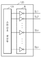
도 3은 본 발명의 일 실시예에 따른 스캔 구동부(120)의 구성을 도시한 것이다.
도 4는 본 발명의 다른 실시예에 따른 표시 장치(100)를 도시한 것이다.
도 5는 본 발명의 다른 실시예에 따른 스캔 구동부(120)의 구성을 도시한 것이다.
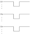
도 6 및 도 7은 스캔 라인에 인가되는 스캔 신호의 예를 도시한 것이다.
도 8 본 발명의 일 실시예에 따른 버퍼의 구성을 도시한 것이다.
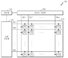
110, 210: 표시 패널
120, 220: 스캔 구동부
130, 230: 데이터 구동부
140, 240: 제어부
PX: 화소
B: 버퍼
SL1~SLn: 스캔 라인
DL1~DLn: 데이터 라인
Claims (20)
- 복수의 스캔 라인 및 상기 스캔 라인에 연결된 복수의 화소를 포함하는 표시 패널; 및
상기 복수의 스캔 라인을 통해 복수의 화소에 스캔 신호를 공급하는 스캔 구동부;를 포함하고,
상기 스캔 구동부는,
상기 스캔 라인 각각에 공급될 스캔 신호를 생성하는 스캔 신호 생성부;
상기 스캔 라인 각각에 대응하여 구비되고, 상기 스캔 신호를 상기 각 스캔 라인으로 출력하는 복수의 버퍼;를 포함하고,
상기 복수의 버퍼 각각에 포함된 트랜지스터의 크기는 상기 버퍼의 출력단에 연결된 회로의 부하에 대응되는
표시 장치.
- 제1 항에 있어서,
상기 트랜지스터의 크기는 상기 트랜지스터의 채널 폭과 길이의 비(W/L)를 의미하는
표시 장치.
- 제1 항에 있어서,
상기 트랜지스터의 크기는 상기 버퍼를 통해 출력되는 스캔 신호를 공급받는 스캔 라인의 부하에 대응하여 형성된
표시 장치.
- 제3 항에 있어서,
상기 트랜지스터의 크기는 상기 스캔 라인에 연결된 화소의 개수에 대응하여 형성된
표시 장치.
- 제4 항에 있어서,
상기 트랜지스터의 크기는 상기 화소의 개수가 많을수록 크게 형성된
표시 장치.
- 제1 항에 있어서,
상기 트랜지스터의 크기는 상기 회로의 부하가 클수록 크게 형성된
표시 장치.
- 제1 항에 있어서,
상기 버퍼로부터 스캔 신호를 공급받는 스캔 라인이 상기 표시 패널의 중앙에 위치할수록 상기 트랜지스터의 크기가 크게 형성된
표시 장치.
- 제1 항에 있어서,
상기 표시 패널은 원형으로 형성되고, 상기 복수의 스캔 라인들 각각에 연결된 화소의 개수는 동일하지 않고,
상기 트랜지스터의 크기는 상기 버퍼의 출력단에 연결된 스캔 라인에 연결된 화소의 개수에 대응하여 형성된
표시 장치.
- 제8 항에 있어서,
상기 스캔 라인이 상기 표시 패널의 중앙에 위치할수록 상기 스캔 라인에 연결된 화소의 개수가 증가하고,
상기 트랜지스터의 크기는 상기 스캔 라인이 상기 표시 패널의 중앙에 위치할수록 크게 형성된
표시 장치.
- 제1 항에 있어서,
상기 트랜지스터의 크기는 상기 회로의 시정수가 클수록 크게 형성된
표시 장치.
- 표시 패널에 스캔 신호를 공급하는 스캔 구동 장치에 있어서,
상기 표시 패널은 복수의 스캔 라인 및 상기 스캔 라인에 연결된 복수의 화소를 포함하고,
상기 스캔 구동 장치는
상기 스캔 라인 각각을 통해 복수의 화소에 공급될 스캔 신호를 생성하는 스캔 신호 생성부;
상기 스캔 라인 각각에 대응하여 구비되고, 상기 스캔 신호를 상기 각 스캔 라인으로 출력하는 복수의 버퍼;를 포함하고,
상기 복수의 버퍼 각각에 포함된 트랜지스터의 크기는 상기 버퍼의 출력단에 연결된 회로의 부하에 대응되는
스캔 구동 장치.
- 제11 항에 있어서,
상기 트랜지스터의 크기는 상기 트랜지스터의 채널 폭과 길이의 비(W/L)를 의미하는
스캔 구동 장치.
- 제11 항에 있어서,
상기 트랜지스터의 크기는 상기 버퍼를 통해 출력되는 스캔 신호를 공급받는 스캔 라인의 부하에 대응하여 형성된
스캔 구동 장치.
- 제13 항에 있어서,
상기 트랜지스터의 크기는 상기 스캔 라인에 연결된 화소의 개수에 대응하여 형성된
스캔 구동 장치.
- 제14 항에 있어서,
상기 트랜지스터의 크기는 상기 화소의 개수가 많을수록 크게 형성된
스캔 구동 장치.
- 제11 항에 있어서,
상기 트랜지스터의 크기는 상기 회로의 부하가 클수록 크게 형성된
스캔 구동 장치.
- 제11 항에 있어서,
상기 버퍼로부터 스캔 신호를 공급받는 스캔 라인이 상기 표시 패널의 중앙에 위치할수록 상기 트랜지스터의 크기가 크게 형성된
스캔 구동 장치.
- 제11 항에 있어서,
상기 표시 패널은 원형으로 형성되고, 상기 복수의 스캔 라인들 각각에 연결된 화소의 개수는 동일하지 않고,
상기 트랜지스터의 크기는 상기 버퍼의 출력단에 연결된 스캔 라인에 연결된 화소의 개수에 대응하여 형성된
스캔 구동 장치.
- 제18 항에 있어서,
상기 스캔 라인이 상기 표시 패널의 중앙에 위치할수록 상기 스캔 라인에 연결된 화소의 개수가 증가하고,
상기 트랜지스터의 크기는 상기 스캔 라인이 상기 표시 패널의 중앙에 위치할수록 크게 형성된
스캔 구동 장치.
- 제11 항에 있어서,
상기 트랜지스터의 크기는 상기 회로의 시정수가 클수록 크게 형성된
스캔 구동 장치.
Priority Applications (2)
| Application Number | Priority Date | Filing Date | Title |
|---|---|---|---|
| KR1020140148437A KR102244075B1 (ko) | 2014-10-29 | 2014-10-29 | 스캔 구동 장치 및 이를 이용한 표시 장치 |
| US14/699,194 US9666127B2 (en) | 2014-10-29 | 2015-04-29 | Scan driving apparatus and display apparatus including the same |
Applications Claiming Priority (1)
| Application Number | Priority Date | Filing Date | Title |
|---|---|---|---|
| KR1020140148437A KR102244075B1 (ko) | 2014-10-29 | 2014-10-29 | 스캔 구동 장치 및 이를 이용한 표시 장치 |
Publications (2)
| Publication Number | Publication Date |
|---|---|
| KR20160052940A true KR20160052940A (ko) | 2016-05-13 |
| KR102244075B1 KR102244075B1 (ko) | 2021-04-26 |
Family
ID=55853346
Family Applications (1)
| Application Number | Title | Priority Date | Filing Date |
|---|---|---|---|
| KR1020140148437A Active KR102244075B1 (ko) | 2014-10-29 | 2014-10-29 | 스캔 구동 장치 및 이를 이용한 표시 장치 |
Country Status (2)
| Country | Link |
|---|---|
| US (1) | US9666127B2 (ko) |
| KR (1) | KR102244075B1 (ko) |
Cited By (2)
| Publication number | Priority date | Publication date | Assignee | Title |
|---|---|---|---|---|
| KR20190142796A (ko) * | 2018-06-18 | 2019-12-30 | 삼성디스플레이 주식회사 | 수평 라인 드라이버 및 이를 포함하는 표시 장치 |
| US10896645B2 (en) | 2016-10-10 | 2021-01-19 | Samsung Display Co., Ltd. | Foldable display device |
Families Citing this family (8)
| Publication number | Priority date | Publication date | Assignee | Title |
|---|---|---|---|---|
| KR20180018930A (ko) * | 2016-08-11 | 2018-02-22 | 삼성디스플레이 주식회사 | 표시장치 및 그의 구동방법 |
| CN108073003B (zh) | 2016-11-09 | 2020-08-18 | 元太科技工业股份有限公司 | 显示面板、像素阵列衬底与线路阵列结构 |
| US10984709B2 (en) | 2018-04-27 | 2021-04-20 | Innolux Corporation | Display panel |
| CN109285494B (zh) * | 2018-10-31 | 2021-10-15 | 厦门天马微电子有限公司 | 异形阵列基板、显示面板和显示装置 |
| CN111583865B (zh) * | 2020-06-12 | 2021-11-26 | 京东方科技集团股份有限公司 | 显示面板、显示装置及开关器件的沟道宽长比的确定方法 |
| CN113946078B (zh) | 2020-07-17 | 2024-11-12 | 群创光电股份有限公司 | 显示装置 |
| JP7664699B2 (ja) * | 2020-12-24 | 2025-04-18 | 武漢天馬微電子有限公司 | 表示装置 |
| US12376234B2 (en) | 2022-01-05 | 2025-07-29 | Innolux Corporation | Communication device |
Citations (3)
| Publication number | Priority date | Publication date | Assignee | Title |
|---|---|---|---|---|
| JP2007310311A (ja) * | 2006-05-22 | 2007-11-29 | Sony Corp | 表示装置及びその駆動方法 |
| JP2011145622A (ja) * | 2010-01-18 | 2011-07-28 | Toshiba Mobile Display Co Ltd | 表示装置および表示装置の駆動方法 |
| US20130120339A1 (en) * | 2011-11-11 | 2013-05-16 | Sony Corporation | Buffer circuit, scanning circuit, display device, and electronic equipment |
Family Cites Families (7)
| Publication number | Priority date | Publication date | Assignee | Title |
|---|---|---|---|---|
| CA2443206A1 (en) | 2003-09-23 | 2005-03-23 | Ignis Innovation Inc. | Amoled display backplanes - pixel driver circuits, array architecture, and external compensation |
| KR100761156B1 (ko) | 2004-02-03 | 2007-09-21 | 엘지전자 주식회사 | 일렉트로-루미네센스 표시소자의 구동장치 및 방법 |
| JP2009069768A (ja) | 2007-09-18 | 2009-04-02 | Toshiba Matsushita Display Technology Co Ltd | 液晶表示装置 |
| JP2009237558A (ja) * | 2008-03-05 | 2009-10-15 | Semiconductor Energy Lab Co Ltd | 半導体装置の駆動方法 |
| KR101663565B1 (ko) | 2010-07-06 | 2016-10-07 | 엘지디스플레이 주식회사 | 액정표시장치 |
| KR102070660B1 (ko) | 2012-04-20 | 2020-01-30 | 삼성디스플레이 주식회사 | 표시 패널 및 이를 포함하는 표시 장치 |
| JP2015102793A (ja) * | 2013-11-27 | 2015-06-04 | 株式会社ジャパンディスプレイ | 表示装置及び表示装置の駆動方法 |
-
2014
- 2014-10-29 KR KR1020140148437A patent/KR102244075B1/ko active Active
-
2015
- 2015-04-29 US US14/699,194 patent/US9666127B2/en active Active
Patent Citations (4)
| Publication number | Priority date | Publication date | Assignee | Title |
|---|---|---|---|---|
| JP2007310311A (ja) * | 2006-05-22 | 2007-11-29 | Sony Corp | 表示装置及びその駆動方法 |
| JP2011145622A (ja) * | 2010-01-18 | 2011-07-28 | Toshiba Mobile Display Co Ltd | 表示装置および表示装置の駆動方法 |
| US20130120339A1 (en) * | 2011-11-11 | 2013-05-16 | Sony Corporation | Buffer circuit, scanning circuit, display device, and electronic equipment |
| JP2013106120A (ja) * | 2011-11-11 | 2013-05-30 | Sony Corp | バッファ回路、走査回路、表示装置、及び、電子機器 |
Cited By (3)
| Publication number | Priority date | Publication date | Assignee | Title |
|---|---|---|---|---|
| US10896645B2 (en) | 2016-10-10 | 2021-01-19 | Samsung Display Co., Ltd. | Foldable display device |
| KR20190142796A (ko) * | 2018-06-18 | 2019-12-30 | 삼성디스플레이 주식회사 | 수평 라인 드라이버 및 이를 포함하는 표시 장치 |
| CN112639942A (zh) * | 2018-06-18 | 2021-04-09 | 三星显示有限公司 | 水平线驱动器以及包括其的显示装置 |
Also Published As
| Publication number | Publication date |
|---|---|
| KR102244075B1 (ko) | 2021-04-26 |
| US9666127B2 (en) | 2017-05-30 |
| US20160125844A1 (en) | 2016-05-05 |
Similar Documents
| Publication | Publication Date | Title |
|---|---|---|
| KR102244075B1 (ko) | 스캔 구동 장치 및 이를 이용한 표시 장치 | |
| US10319306B2 (en) | Pixel, organic light emitting display device using the same, and method of driving the organic light emitting display device | |
| US9812062B2 (en) | Display apparatus and method of driving the same | |
| GB2560082B (en) | Organic light emitting display panel and organic light emitting display device including the same | |
| US9583041B2 (en) | Pixel circuit and driving method thereof, display panel, and display device | |
| US9646541B2 (en) | Display device | |
| CN100551183C (zh) | 像素和使用该像素的有机发光显示装置 | |
| US9087480B2 (en) | Scan lines driver and organic light emmiting display device using the same | |
| US9564082B2 (en) | Array substrate, display device and driving method thereof | |
| CN102654975B (zh) | Amoled驱动补偿电路、方法及其显示装置 | |
| KR102293982B1 (ko) | 표시 회로 및 표시 장치 | |
| KR20210086801A (ko) | 표시 장치 | |
| CN104505024B (zh) | 一种显示驱动方法、显示面板和显示装置 | |
| CN114999390A (zh) | 像素 | |
| KR102748937B1 (ko) | 발광 제어 구동부 및 이를 포함하는 표시 장치 | |
| US8847934B2 (en) | Displaying apparatus | |
| CN107967896A (zh) | 像素补偿电路 | |
| WO2018032899A1 (zh) | 像素电路及其驱动方法、显示面板和显示装置 | |
| KR20140077359A (ko) | 표시장치와 그 게이트 구동회로의 제어 방법 | |
| KR20150107995A (ko) | 유기 발광 표시 장치, 및 유기 발광 표시 장치의 구동 방법 | |
| KR20120028005A (ko) | 발광제어 구동부 및 그를 이용한 유기전계발광 표시장치 | |
| CN110796987A (zh) | 显示装置及使用其驱动显示面板的方法 | |
| CN106991971A (zh) | 显示装置、栅极驱动电路及其驱动方法 | |
| JP2020533615A (ja) | 画素補償回路ユニット、画素回路および表示装置 | |
| CN101763807A (zh) | 发光元件的驱动装置 |
Legal Events
| Date | Code | Title | Description |
|---|---|---|---|
| PA0109 | Patent application |
St.27 status event code: A-0-1-A10-A12-nap-PA0109 |
|
| R18-X000 | Changes to party contact information recorded |
St.27 status event code: A-3-3-R10-R18-oth-X000 |
|
| PG1501 | Laying open of application |
St.27 status event code: A-1-1-Q10-Q12-nap-PG1501 |
|
| R18-X000 | Changes to party contact information recorded |
St.27 status event code: A-3-3-R10-R18-oth-X000 |
|
| A201 | Request for examination | ||
| PA0201 | Request for examination |
St.27 status event code: A-1-2-D10-D11-exm-PA0201 |
|
| E902 | Notification of reason for refusal | ||
| PE0902 | Notice of grounds for rejection |
St.27 status event code: A-1-2-D10-D21-exm-PE0902 |
|
| E13-X000 | Pre-grant limitation requested |
St.27 status event code: A-2-3-E10-E13-lim-X000 |
|
| P11-X000 | Amendment of application requested |
St.27 status event code: A-2-2-P10-P11-nap-X000 |
|
| P13-X000 | Application amended |
St.27 status event code: A-2-2-P10-P13-nap-X000 |
|
| E701 | Decision to grant or registration of patent right | ||
| PE0701 | Decision of registration |
St.27 status event code: A-1-2-D10-D22-exm-PE0701 |
|
| GRNT | Written decision to grant | ||
| PR0701 | Registration of establishment |
St.27 status event code: A-2-4-F10-F11-exm-PR0701 |
|
| PR1002 | Payment of registration fee |
St.27 status event code: A-2-2-U10-U11-oth-PR1002 Fee payment year number: 1 |
|
| PG1601 | Publication of registration |
St.27 status event code: A-4-4-Q10-Q13-nap-PG1601 |
|
| PR1001 | Payment of annual fee |
St.27 status event code: A-4-4-U10-U11-oth-PR1001 Fee payment year number: 4 |
|
| PR1001 | Payment of annual fee |
St.27 status event code: A-4-4-U10-U11-oth-PR1001 Fee payment year number: 5 |
|
| PR1001 | Payment of annual fee |
St.27 status event code: A-4-4-U10-U11-oth-PR1001 Fee payment year number: 6 |
|
| U11 | Full renewal or maintenance fee paid |
Free format text: ST27 STATUS EVENT CODE: A-4-4-U10-U11-OTH-PR1001 (AS PROVIDED BY THE NATIONAL OFFICE) Year of fee payment: 6 |