KR20160052943A - 박막 트랜지스터 기판 - Google Patents
박막 트랜지스터 기판 Download PDFInfo
- Publication number
- KR20160052943A KR20160052943A KR1020140148449A KR20140148449A KR20160052943A KR 20160052943 A KR20160052943 A KR 20160052943A KR 1020140148449 A KR1020140148449 A KR 1020140148449A KR 20140148449 A KR20140148449 A KR 20140148449A KR 20160052943 A KR20160052943 A KR 20160052943A
- Authority
- KR
- South Korea
- Prior art keywords
- pixel
- line
- pixels
- thin film
- pixel row
- Prior art date
- Legal status (The legal status is an assumption and is not a legal conclusion. Google has not performed a legal analysis and makes no representation as to the accuracy of the status listed.)
- Granted
Links
Images



Classifications
-
- G—PHYSICS
- G09—EDUCATION; CRYPTOGRAPHY; DISPLAY; ADVERTISING; SEALS
- G09G—ARRANGEMENTS OR CIRCUITS FOR CONTROL OF INDICATING DEVICES USING STATIC MEANS TO PRESENT VARIABLE INFORMATION
- G09G3/00—Control arrangements or circuits, of interest only in connection with visual indicators other than cathode-ray tubes
- G09G3/20—Control arrangements or circuits, of interest only in connection with visual indicators other than cathode-ray tubes for presentation of an assembly of a number of characters, e.g. a page, by composing the assembly by combination of individual elements arranged in a matrix no fixed position being assigned to or needed to be assigned to the individual characters or partial characters
- G09G3/22—Control arrangements or circuits, of interest only in connection with visual indicators other than cathode-ray tubes for presentation of an assembly of a number of characters, e.g. a page, by composing the assembly by combination of individual elements arranged in a matrix no fixed position being assigned to or needed to be assigned to the individual characters or partial characters using controlled light sources
- G09G3/30—Control arrangements or circuits, of interest only in connection with visual indicators other than cathode-ray tubes for presentation of an assembly of a number of characters, e.g. a page, by composing the assembly by combination of individual elements arranged in a matrix no fixed position being assigned to or needed to be assigned to the individual characters or partial characters using controlled light sources using electroluminescent panels
- G09G3/32—Control arrangements or circuits, of interest only in connection with visual indicators other than cathode-ray tubes for presentation of an assembly of a number of characters, e.g. a page, by composing the assembly by combination of individual elements arranged in a matrix no fixed position being assigned to or needed to be assigned to the individual characters or partial characters using controlled light sources using electroluminescent panels semiconductive, e.g. using light-emitting diodes [LED]
- G09G3/3208—Control arrangements or circuits, of interest only in connection with visual indicators other than cathode-ray tubes for presentation of an assembly of a number of characters, e.g. a page, by composing the assembly by combination of individual elements arranged in a matrix no fixed position being assigned to or needed to be assigned to the individual characters or partial characters using controlled light sources using electroluminescent panels semiconductive, e.g. using light-emitting diodes [LED] organic, e.g. using organic light-emitting diodes [OLED]
- G09G3/3225—Control arrangements or circuits, of interest only in connection with visual indicators other than cathode-ray tubes for presentation of an assembly of a number of characters, e.g. a page, by composing the assembly by combination of individual elements arranged in a matrix no fixed position being assigned to or needed to be assigned to the individual characters or partial characters using controlled light sources using electroluminescent panels semiconductive, e.g. using light-emitting diodes [LED] organic, e.g. using organic light-emitting diodes [OLED] using an active matrix
- G09G3/3258—Control arrangements or circuits, of interest only in connection with visual indicators other than cathode-ray tubes for presentation of an assembly of a number of characters, e.g. a page, by composing the assembly by combination of individual elements arranged in a matrix no fixed position being assigned to or needed to be assigned to the individual characters or partial characters using controlled light sources using electroluminescent panels semiconductive, e.g. using light-emitting diodes [LED] organic, e.g. using organic light-emitting diodes [OLED] using an active matrix with pixel circuitry controlling the voltage across the light-emitting element
-
- G—PHYSICS
- G02—OPTICS
- G02F—OPTICAL DEVICES OR ARRANGEMENTS FOR THE CONTROL OF LIGHT BY MODIFICATION OF THE OPTICAL PROPERTIES OF THE MEDIA OF THE ELEMENTS INVOLVED THEREIN; NON-LINEAR OPTICS; FREQUENCY-CHANGING OF LIGHT; OPTICAL LOGIC ELEMENTS; OPTICAL ANALOGUE/DIGITAL CONVERTERS
- G02F1/00—Devices or arrangements for the control of the intensity, colour, phase, polarisation or direction of light arriving from an independent light source, e.g. switching, gating or modulating; Non-linear optics
- G02F1/01—Devices or arrangements for the control of the intensity, colour, phase, polarisation or direction of light arriving from an independent light source, e.g. switching, gating or modulating; Non-linear optics for the control of the intensity, phase, polarisation or colour
- G02F1/13—Devices or arrangements for the control of the intensity, colour, phase, polarisation or direction of light arriving from an independent light source, e.g. switching, gating or modulating; Non-linear optics for the control of the intensity, phase, polarisation or colour based on liquid crystals, e.g. single liquid crystal display cells
-
- G—PHYSICS
- G09—EDUCATION; CRYPTOGRAPHY; DISPLAY; ADVERTISING; SEALS
- G09G—ARRANGEMENTS OR CIRCUITS FOR CONTROL OF INDICATING DEVICES USING STATIC MEANS TO PRESENT VARIABLE INFORMATION
- G09G2300/00—Aspects of the constitution of display devices
- G09G2300/04—Structural and physical details of display devices
- G09G2300/0421—Structural details of the set of electrodes
- G09G2300/043—Compensation electrodes or other additional electrodes in matrix displays related to distortions or compensation signals, e.g. for modifying TFT threshold voltage in column driver
-
- G—PHYSICS
- G09—EDUCATION; CRYPTOGRAPHY; DISPLAY; ADVERTISING; SEALS
- G09G—ARRANGEMENTS OR CIRCUITS FOR CONTROL OF INDICATING DEVICES USING STATIC MEANS TO PRESENT VARIABLE INFORMATION
- G09G2300/00—Aspects of the constitution of display devices
- G09G2300/08—Active matrix structure, i.e. with use of active elements, inclusive of non-linear two terminal elements, in the pixels together with light emitting or modulating elements
- G09G2300/0809—Several active elements per pixel in active matrix panels
-
- G—PHYSICS
- G09—EDUCATION; CRYPTOGRAPHY; DISPLAY; ADVERTISING; SEALS
- G09G—ARRANGEMENTS OR CIRCUITS FOR CONTROL OF INDICATING DEVICES USING STATIC MEANS TO PRESENT VARIABLE INFORMATION
- G09G2310/00—Command of the display device
- G09G2310/02—Addressing, scanning or driving the display screen or processing steps related thereto
- G09G2310/0202—Addressing of scan or signal lines
- G09G2310/0216—Interleaved control phases for different scan lines in the same sub-field, e.g. initialization, addressing and sustaining in plasma displays that are not simultaneous for all scan lines
-
- G—PHYSICS
- G09—EDUCATION; CRYPTOGRAPHY; DISPLAY; ADVERTISING; SEALS
- G09G—ARRANGEMENTS OR CIRCUITS FOR CONTROL OF INDICATING DEVICES USING STATIC MEANS TO PRESENT VARIABLE INFORMATION
- G09G2310/00—Command of the display device
- G09G2310/02—Addressing, scanning or driving the display screen or processing steps related thereto
- G09G2310/0202—Addressing of scan or signal lines
- G09G2310/0218—Addressing of scan or signal lines with collection of electrodes in groups for n-dimensional addressing
-
- G—PHYSICS
- G09—EDUCATION; CRYPTOGRAPHY; DISPLAY; ADVERTISING; SEALS
- G09G—ARRANGEMENTS OR CIRCUITS FOR CONTROL OF INDICATING DEVICES USING STATIC MEANS TO PRESENT VARIABLE INFORMATION
- G09G2310/00—Command of the display device
- G09G2310/02—Addressing, scanning or driving the display screen or processing steps related thereto
- G09G2310/0262—The addressing of the pixel, in a display other than an active matrix LCD, involving the control of two or more scan electrodes or two or more data electrodes, e.g. pixel voltage dependent on signals of two data electrodes
-
- G—PHYSICS
- G09—EDUCATION; CRYPTOGRAPHY; DISPLAY; ADVERTISING; SEALS
- G09G—ARRANGEMENTS OR CIRCUITS FOR CONTROL OF INDICATING DEVICES USING STATIC MEANS TO PRESENT VARIABLE INFORMATION
- G09G2320/00—Control of display operating conditions
- G09G2320/02—Improving the quality of display appearance
- G09G2320/0242—Compensation of deficiencies in the appearance of colours
-
- G—PHYSICS
- G09—EDUCATION; CRYPTOGRAPHY; DISPLAY; ADVERTISING; SEALS
- G09G—ARRANGEMENTS OR CIRCUITS FOR CONTROL OF INDICATING DEVICES USING STATIC MEANS TO PRESENT VARIABLE INFORMATION
- G09G2320/00—Control of display operating conditions
- G09G2320/04—Maintaining the quality of display appearance
- G09G2320/043—Preventing or counteracting the effects of ageing
- G09G2320/045—Compensation of drifts in the characteristics of light emitting or modulating elements
Landscapes
- Physics & Mathematics (AREA)
- Engineering & Computer Science (AREA)
- General Physics & Mathematics (AREA)
- Nonlinear Science (AREA)
- Computer Hardware Design (AREA)
- Theoretical Computer Science (AREA)
- Chemical & Material Sciences (AREA)
- Crystallography & Structural Chemistry (AREA)
- Optics & Photonics (AREA)
- Control Of El Displays (AREA)
- Electroluminescent Light Sources (AREA)
Abstract
본 발명의 일 실시예에 따른 박막 트랜지스터 기판은, 제1 화소 행에 배치된 복수의 제1 화소들; 상기 제1 화소 행에 인접한 제2 화소 행에 배치된 복수의 제2 화소들; 상기 제2 화소 행에 인접한 제3 화소 행에 배치된 복수의 제3 화소들; 상기 제1 화소 행과 제2 화소 행 사이에 배치되고, 상기 복수의 제1 화소들과 제2 화소들에 제1 초기화 전압을 인가하는 제1 초기화 전압선; 및 상기 제2 화소 행과 상기 제3화소 행 사이에 배치되고, 상기 복수의 제2 화소들과 제3 화소들에 상기 제1 초기화 전압과 다른 레벨의 제2 초기화 전압을 인가하는 제2 초기화 전압선;을 포함한다.
Description
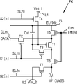
도 2는 본 발명의 일 실시예에 따른 표시 장치의 하나의 화소의 등가 회로도이다.
도 3은 본 발명의 일 실시예에 따른 유기 발광 표시 장치의 일부 화소를 나타낸 회로도이다.
도 4는 본 발명의 일 실시예에 따른 유기 발광 표시 장치의 일부 화소를 나타낸 평면도이다.
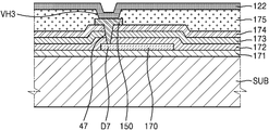
도 5는 도 4에 도시된 제3 비아홀(VH3) 영역의 단면도이다.
Claims (20)
- 제1 화소 행에 배치된 복수의 제1 화소들;
상기 제1 화소 행에 인접한 제2 화소 행에 배치된 복수의 제2 화소들;
상기 제2 화소 행에 인접한 제3 화소 행에 배치된 복수의 제3 화소들;
상기 제1 화소 행과 제2 화소 행 사이에 배치되고, 상기 복수의 제1 화소들과 제2 화소들에 제1 초기화 전압을 인가하는 제1 초기화 전압선; 및
상기 제2 화소 행과 상기 제3화소 행 사이에 배치되고, 상기 복수의 제2 화소들과 제3 화소들에 상기 제1 초기화 전압과 다른 레벨의 제2 초기화 전압을 인가하는 제2 초기화 전압선;을 포함하는 박막 트랜지스터 기판. - 제1항에 있어서,
동일 화소 열의 제1 화소와 제2 화소는 상기 제1 초기화 전압선을 기준으로 대칭인 박막 트랜지스터 기판. - 제1항에 있어서,
동일 화소 열의 제2 화소와 제3 화소는 상기 제2 초기화 전압선을 기준으로 대칭인 박막 트랜지스터 기판. - 제1항에 있어서
상기 제1 초기화 전압선을 인접한 두 개의 화소 열에 배치된 한 쌍의 제1 화소들 및 한 쌍의 제2 화소들과 전기적으로 연결하는 제1 연결 전극;을 더 포함하는 박막 트랜지스터 기판. - 제4항에 있어서,
상기 인접한 두 개의 화소 열의 제1 화소들 내지 제2 화소들 각각의 초기화 박막 트랜지스터와 연결된 제1 활성층 연결선;
상기 제1 활성층 연결선과 상기 제1 연결 전극 사이에 형성되고, 제1 공통 컨택홀을 구비한 제1 절연막; 및
상기 제1 연결 전극 상부에 차례로 형성되고, 제1 비아홀을 구비한 제2 절연막과 제3 절연막;을 더 포함하고,
상기 초기화 박막 트랜지스터는 상기 제1 초기화 전압을 전달하고,
상기 제1 연결 전극은 상기 제1 공통 컨택홀을 통해 상기 제1 활성층 연결선과 컨택하고,
상기 제1 초기화 전압선은 상기 제3 절연막 상부에 형성되고, 상기 제1 비아홀을 통해 상기 제1 연결 전극과 컨택하는 박막 트랜지스터 기판. - 제1항에 있어서,
상기 제2 초기화 전압선을 인접한 두 개의 화소 열에 배치된 한 쌍의 제2 화소들 및 한 쌍의 제3 화소들과 전기적으로 연결하는 제2 연결 전극;을 더 포함하는 박막 트랜지스터 기판. - 제6항에 있어서,
상기 인접한 두 개의 화소 열의 제2 화소들 내지 제3 화소들 각각의 바이패스 박막 트랜지스터와 연결된 제2 활성층 연결선;
상기 제2 활성층 연결선과 상기 제2 연결 전극 사이에 형성되고, 제2 공통 컨택홀을 구비한 제1 절연막; 및
상기 제2 연결 전극 상부에 차례로 형성되고, 제2 비아홀을 구비한 제2 절연막과 제3 절연막;을 더 포함하고,
상기 바이패스 박막 트랜지스터는 상기 제2 초기화 전압을 전달하고,
상기 제2 연결 전극은 상기 제2 공통 컨택홀을 통해 상기 제2 활성층 연결선과 컨택하고,
상기 제2 초기화 전압선은 상기 제3 절연막 상부에 형성되고, 상기 제2 비아홀을 통해 상기 제2 연결 전극과 컨택하는 박막 트랜지스터 기판. - 제1항에 있어서,
상기 제1 화소 행 내지 제3 화소 행 각각에 배치되어 상기 제1 화소들 내지 제3 화소들로 제1 주사신호 및 제2 주사신호를 각각 인가하는 제1 주사선들 및 제2 주사선들;
상기 제1 주사선들 및 제2 주사선들과 교차하며 화소 열마다 배치되고, 상기 제1 화소들 내지 제3 화소들로 데이터 신호를 인가하는 데이터선들; 및
상기 제1 주사선들 및 제2 주사선들과 교차하며 화소 열마다 배치되고, 상기 제1 화소들 내지 제3 화소들로 제1 전원전압을 인가하는 구동전압선들;을 더 포함하는 박막 트랜지스터 기판. - 제8항에 있어서,
상기 제1 화소 행의 제1 주사선 및 제2 주사선은 상기 제1 초기화 전압선을 기준으로 상기 제2 화소 행의 제1 주사선 및 제2 주사선과 대칭인 박막 트랜지스터 기판. - 제8항에 있어서,
상기 제2 화소 행의 제1 주사선 및 제2 주사선은 상기 제2 초기화 전압선을 기준으로 상기 제3 화소 행의 제1 주사선 및 제2 주사선과 대칭인 박막 트랜지스터 기판. - 복수의 화소들을 포함하는 박막 트랜지스터 기판에 있어서,
상기 복수의 화소들 각각은,
제1 주사 신호에 응답하여 데이터 신호에 대응하는 구동전류를 발광소자로 출력하는 구동 박막 트랜지스터;
제2 주사 신호에 응답하여 제1 초기화 전압을 상기 구동 박막 트랜지스터의 게이트 전극으로 전달하는 초기화 박막 트랜지스터; 및
상기 제2 주사 신호에 응답하여 상기 제1 초기화 전압과 다른 레벨의 제2 초기화 전압을 상기 발광소자의 애노드 전극으로 전달하는 바이패스 박막 트랜지스터;를 포함하고,
상기 복수의 화소들 각각은 상기 제1 초기화 전압을 공급하는 제1 초기화 전압선 및 상기 제2 초기화 전압을 공급하는 제2 초기화 전압선에 연결되고,
상기 제1 초기화 전압선은 동일 화소 행의 인접 화소들 및 인접한 제1 화소 행의 화소들의 초기화 박막 트랜지스터들과 연결되고, 상기 동일 화소 행과 제1 화소 행 사이에 배치되고,
상기 제2 초기화 전압선은 동일 화소 행의 인접 화소들 및 인접한 제2 화소 행의 화소들의 바이패스 박막 트랜지스터들과 연결되고, 상기 동일 화소 행과 제2 화소 행 사이에 배치된, 박막 트랜지스터 기판. - 제11항에 있어서,
상기 복수의 화소들 각각은 동일 화소 열의 상기 제1 화소 행의 화소와 상기 제1 초기화 전압선을 기준으로 대칭인 박막 트랜지스터 기판. - 제11항에 있어서,
상기 복수의 화소들 각각은 동일 화소 열의 상기 제2 화소 행의 화소와 상기 제2 초기화 전압선을 기준으로 대칭인 박막 트랜지스터 기판. - 제11항에 있어서
상기 제1 초기화 전압선을 인접한 두 개의 화소 열에 배치된 동일 화소 행의 한 쌍의 화소들 및 제1 화소 행의 한 쌍의 화소들과 전기적으로 연결하는 제1 연결 전극;을 더 포함하는 박막 트랜지스터 기판. - 제11항에 있어서,
상기 제2 초기화 전압선을 인접한 두 개의 화소 열에 배치된 동일 화소 행의 한 쌍의 화소들 및 제2 화소 행의 한 쌍의 화소들과 전기적으로 연결하는 제2 연결 전극;을 더 포함하는 박막 트랜지스터 기판. - 제1 화소 행에 배치된 제1 화소 및 제2 화소;
상기 제1 화소 행에 인접한 제2 화소 행에 배치되고, 상기 제1 화소와 동일 화소 열에 배치된 제3 화소 및 상기 제2 화소와 동일 화소 열에 배치된 제4 화소;
상기 제2 화소 행에 인접한 제3 화소 행에 배치되고, 상기 제1 화소와 동일 화소 열에 배치된 제5 화소 및 상기 제2 화소와 동일 화소 열에 배치된 제6 화소;
상기 제1 화소 행과 상기 제2 화소 행 사이에 배치되고, 상기 제1 화소 내지 상기 제4 화소에 제1 초기화 전압을 인가하는 제1 초기화 전압선; 및
상기 제2 화소 행과 상기 제3 화소 행 사이에 배치되고, 상기 제3 화소 내지 제6 화소에 상기 제1 초기화 전압과 다른 레벨의 제2 초기화 전압을 인가하는 제2 초기화 전압선;을 포함하는 박막 트랜지스터 기판. - 제16항에 있어서,
상기 제1 화소 및 제2 화소는 각각 상기 제1 초기화 전압선을 기준으로 상기 제3 화소 및 제4 화소와 대칭인 박막 트랜지스터 기판. - 제16항에 있어서,
상기 제3 화소 및 제4 화소는 각각 상기 제2 초기화 전압선을 기준으로 상기 제5 화소 및 제6 화소와 대칭인 박막 트랜지스터 기판. - 제16항에 있어서
상기 제1 초기화 전압선을 상기 제1 화소 내지 제4 화소에 전기적으로 연결하는 제1 연결 전극;을 더 포함하는 박막 트랜지스터 기판. - 제16항에 있어서,
상기 제2 초기화 전압선을 상기 제3 화소 내지 제6 화소에 전기적으로 연결하는 제2 연결 전극;을 더 포함하는 박막 트랜지스터 기판.
Priority Applications (2)
| Application Number | Priority Date | Filing Date | Title |
|---|---|---|---|
| KR1020140148449A KR102305682B1 (ko) | 2014-10-29 | 2014-10-29 | 박막 트랜지스터 기판 |
| US14/682,451 US20160125809A1 (en) | 2014-10-29 | 2015-04-09 | Thin film transistor substrate |
Applications Claiming Priority (1)
| Application Number | Priority Date | Filing Date | Title |
|---|---|---|---|
| KR1020140148449A KR102305682B1 (ko) | 2014-10-29 | 2014-10-29 | 박막 트랜지스터 기판 |
Publications (2)
| Publication Number | Publication Date |
|---|---|
| KR20160052943A true KR20160052943A (ko) | 2016-05-13 |
| KR102305682B1 KR102305682B1 (ko) | 2021-09-29 |
Family
ID=55853326
Family Applications (1)
| Application Number | Title | Priority Date | Filing Date |
|---|---|---|---|
| KR1020140148449A Active KR102305682B1 (ko) | 2014-10-29 | 2014-10-29 | 박막 트랜지스터 기판 |
Country Status (2)
| Country | Link |
|---|---|
| US (1) | US20160125809A1 (ko) |
| KR (1) | KR102305682B1 (ko) |
Cited By (8)
| Publication number | Priority date | Publication date | Assignee | Title |
|---|---|---|---|---|
| WO2020036307A1 (ko) * | 2018-08-13 | 2020-02-20 | 삼성디스플레이 주식회사 | 픽셀 회로 및 이를 포함하는 표시 장치 |
| KR20200069436A (ko) * | 2018-12-06 | 2020-06-17 | 삼성디스플레이 주식회사 | 표시 장치 |
| KR20210022216A (ko) * | 2019-08-19 | 2021-03-03 | 삼성디스플레이 주식회사 | 표시 장치 |
| US11024237B2 (en) | 2018-01-15 | 2021-06-01 | Samsung Display Co., Ltd. | Pixel and organic light emitting display device including the same |
| US11257897B2 (en) | 2019-08-26 | 2022-02-22 | Samsung Display Co., Ltd. | Display panel including an initialization voltage line and an auxiliary voltage line and display device including the same |
| US11488536B2 (en) | 2020-06-19 | 2022-11-01 | Samsung Display Co., Ltd. | Display apparatus |
| US12057066B2 (en) | 2021-05-12 | 2024-08-06 | Samsung Display Co., Ltd. | Display apparatus |
| US12446416B2 (en) | 2020-08-24 | 2025-10-14 | Samsung Display Co., Ltd. | Organic light-emitting diode display apparatus including first and second initialization connection lines maintaining initialization voltages |
Families Citing this family (22)
| Publication number | Priority date | Publication date | Assignee | Title |
|---|---|---|---|---|
| KR102559544B1 (ko) * | 2016-07-01 | 2023-07-26 | 삼성디스플레이 주식회사 | 표시 장치 |
| KR20180071896A (ko) * | 2016-12-20 | 2018-06-28 | 엘지디스플레이 주식회사 | 유기발광표시장치 및 그의 구동방법 |
| KR102356628B1 (ko) * | 2017-06-21 | 2022-01-28 | 삼성디스플레이 주식회사 | 다면 발광 표시 장치 및 화소 |
| CN107633798B (zh) * | 2017-10-11 | 2020-03-17 | 深圳市华星光电半导体显示技术有限公司 | 电位转换电路及显示面板 |
| KR102527793B1 (ko) * | 2017-10-16 | 2023-05-04 | 삼성디스플레이 주식회사 | 표시 장치 및 그 구동 방법 |
| KR102523646B1 (ko) | 2017-11-01 | 2023-04-21 | 삼성디스플레이 주식회사 | 표시 장치 및 그 구동 방법 |
| KR102632905B1 (ko) * | 2018-07-18 | 2024-02-06 | 삼성디스플레이 주식회사 | 유기 발광 표시 장치 및 이의 구동 방법 |
| KR102583403B1 (ko) | 2018-10-11 | 2023-09-26 | 엘지디스플레이 주식회사 | 디스플레이 장치 및 디스플레이 패널 |
| KR102637057B1 (ko) * | 2019-09-24 | 2024-02-14 | 엘지디스플레이 주식회사 | 디스플레이 장치 |
| KR102681836B1 (ko) * | 2020-03-03 | 2024-07-04 | 삼성디스플레이 주식회사 | 표시장치 |
| KR102942305B1 (ko) * | 2020-05-14 | 2026-03-20 | 삼성디스플레이 주식회사 | 표시장치 |
| WO2022067460A1 (zh) * | 2020-09-29 | 2022-04-07 | 京东方科技集团股份有限公司 | 显示面板及其像素电路的驱动方法、显示装置 |
| CN112289269A (zh) * | 2020-10-30 | 2021-01-29 | 合肥维信诺科技有限公司 | 一种像素电路及其控制方法和显示面板 |
| CN115461806B (zh) * | 2021-03-29 | 2024-10-18 | 京东方科技集团股份有限公司 | 像素电路、显示面板及显示装置 |
| GB2615936A (en) * | 2021-04-23 | 2023-08-23 | Boe Technology Group Co Ltd | Pixel circuit and driving method therefor, and display device |
| WO2022266875A1 (zh) * | 2021-06-23 | 2022-12-29 | 京东方科技集团股份有限公司 | 像素电路、驱动方法和显示装置 |
| KR102830513B1 (ko) | 2021-07-12 | 2025-07-08 | 삼성디스플레이 주식회사 | 화소 및 표시 장치 |
| KR20230023122A (ko) * | 2021-08-09 | 2023-02-17 | 삼성디스플레이 주식회사 | 표시 장치 |
| KR20230109211A (ko) * | 2022-01-12 | 2023-07-20 | 삼성디스플레이 주식회사 | 표시패널 |
| US20250140183A1 (en) * | 2022-04-21 | 2025-05-01 | Chengdu Boe Optoelectronics Technology Co., Ltd. | Display panel and method for driving pixel circuit, and display device |
| KR20240081795A (ko) * | 2022-12-01 | 2024-06-10 | 엘지디스플레이 주식회사 | 화소 회로 및 이를 포함하는 표시 장치 |
| KR20240107890A (ko) * | 2022-12-30 | 2024-07-09 | 엘지디스플레이 주식회사 | 표시 장치 및 구동 방법 |
Citations (3)
| Publication number | Priority date | Publication date | Assignee | Title |
|---|---|---|---|---|
| US20070273621A1 (en) * | 2006-05-29 | 2007-11-29 | Sony Corporation | Image display device |
| US20120001893A1 (en) * | 2010-06-30 | 2012-01-05 | Samsung Mobile Display Co., Ltd. | Pixel and organic light emitting display device using the same |
| US20130257839A1 (en) * | 2012-03-29 | 2013-10-03 | Samsung Display Co., Ltd. | Organic Light Emitting Diode Display |
Family Cites Families (5)
| Publication number | Priority date | Publication date | Assignee | Title |
|---|---|---|---|---|
| US6587086B1 (en) * | 1999-10-26 | 2003-07-01 | Semiconductor Energy Laboratory Co., Ltd. | Electro-optical device |
| KR101762344B1 (ko) * | 2010-07-27 | 2017-07-31 | 삼성디스플레이 주식회사 | 유기 전계 발광 표시 장치 |
| KR102061791B1 (ko) * | 2012-11-13 | 2020-01-03 | 삼성디스플레이 주식회사 | 유기 발광 표시 장치 및 이의 제조 방법 |
| KR102038076B1 (ko) * | 2013-04-04 | 2019-10-30 | 삼성디스플레이 주식회사 | 유기 발광 표시 장치 |
| JP2015125366A (ja) * | 2013-12-27 | 2015-07-06 | 株式会社ジャパンディスプレイ | 表示装置 |
-
2014
- 2014-10-29 KR KR1020140148449A patent/KR102305682B1/ko active Active
-
2015
- 2015-04-09 US US14/682,451 patent/US20160125809A1/en not_active Abandoned
Patent Citations (3)
| Publication number | Priority date | Publication date | Assignee | Title |
|---|---|---|---|---|
| US20070273621A1 (en) * | 2006-05-29 | 2007-11-29 | Sony Corporation | Image display device |
| US20120001893A1 (en) * | 2010-06-30 | 2012-01-05 | Samsung Mobile Display Co., Ltd. | Pixel and organic light emitting display device using the same |
| US20130257839A1 (en) * | 2012-03-29 | 2013-10-03 | Samsung Display Co., Ltd. | Organic Light Emitting Diode Display |
Cited By (17)
| Publication number | Priority date | Publication date | Assignee | Title |
|---|---|---|---|---|
| US11436984B2 (en) | 2018-01-15 | 2022-09-06 | Samsung Display Co., Ltd. | Pixel and organic light emitting display device having the same |
| US11024237B2 (en) | 2018-01-15 | 2021-06-01 | Samsung Display Co., Ltd. | Pixel and organic light emitting display device including the same |
| KR20230117722A (ko) * | 2018-01-15 | 2023-08-09 | 삼성디스플레이 주식회사 | 화소 및 이를 갖는 유기발광 표시장치 |
| CN112585671A (zh) * | 2018-08-13 | 2021-03-30 | 三星显示有限公司 | 像素电路以及具有该像素电路的显示装置 |
| US11386854B2 (en) | 2018-08-13 | 2022-07-12 | Samsung Display Co., Ltd. | Pixel circuit and display apparatus having the same |
| CN112585671B (zh) * | 2018-08-13 | 2024-08-20 | 三星显示有限公司 | 像素电路以及具有该像素电路的显示装置 |
| WO2020036307A1 (ko) * | 2018-08-13 | 2020-02-20 | 삼성디스플레이 주식회사 | 픽셀 회로 및 이를 포함하는 표시 장치 |
| US11094771B2 (en) | 2018-12-06 | 2021-08-17 | Samsung Display Co., Ltd. | Display device with first and second initialization lines |
| KR20200069436A (ko) * | 2018-12-06 | 2020-06-17 | 삼성디스플레이 주식회사 | 표시 장치 |
| KR20210022216A (ko) * | 2019-08-19 | 2021-03-03 | 삼성디스플레이 주식회사 | 표시 장치 |
| US11903278B2 (en) | 2019-08-26 | 2024-02-13 | Samsung Display Co., Ltd. | Display panel including an initialization voltage line and an auxiliary voltage line and display device including the same |
| US11257897B2 (en) | 2019-08-26 | 2022-02-22 | Samsung Display Co., Ltd. | Display panel including an initialization voltage line and an auxiliary voltage line and display device including the same |
| US11488536B2 (en) | 2020-06-19 | 2022-11-01 | Samsung Display Co., Ltd. | Display apparatus |
| US11688350B2 (en) | 2020-06-19 | 2023-06-27 | Samsung Display Co., Ltd. | Display apparatus |
| US12446416B2 (en) | 2020-08-24 | 2025-10-14 | Samsung Display Co., Ltd. | Organic light-emitting diode display apparatus including first and second initialization connection lines maintaining initialization voltages |
| US12057066B2 (en) | 2021-05-12 | 2024-08-06 | Samsung Display Co., Ltd. | Display apparatus |
| US12424169B2 (en) | 2021-05-12 | 2025-09-23 | Samsung Display Co., Ltd. | Display apparatus |
Also Published As
| Publication number | Publication date |
|---|---|
| US20160125809A1 (en) | 2016-05-05 |
| KR102305682B1 (ko) | 2021-09-29 |
Similar Documents
| Publication | Publication Date | Title |
|---|---|---|
| KR102305682B1 (ko) | 박막 트랜지스터 기판 | |
| KR102293409B1 (ko) | 유기 발광 표시 장치 | |
| CN109979394B (zh) | 像素电路及其驱动方法、阵列基板及显示装置 | |
| JP5080733B2 (ja) | 表示装置及びその駆動方法 | |
| US9236484B2 (en) | Thin film transistor, and pixel and organic light emitting display device having the same | |
| US10032412B2 (en) | Organic light emitting diode pixel driving circuit, display panel and display device | |
| JP5135519B2 (ja) | 有機電界発光表示装置 | |
| US9437136B2 (en) | Light-emitting display apparatus and driving method thereof | |
| US9704433B2 (en) | Organic light emitting display and method for driving the same | |
| US9514677B2 (en) | Display device and driving method thereof | |
| EP2626904A2 (en) | Organic light emitting diode display | |
| US20050052366A1 (en) | Circuit and method for driving pixel of organic electroluminescent display | |
| KR102484383B1 (ko) | 유기발광다이오드 표시패널 및 이의 표시장치 | |
| KR20180081655A (ko) | 유기발광 표시장치 | |
| US9336715B2 (en) | Pixel, display device and driving method with simultaneous writing and emisson | |
| KR20140067583A (ko) | 유기 발광 다이오드 표시장치 및 그 구동 방법 | |
| US9183784B2 (en) | Display device and driving method thereof for compensating a threshold voltage deviation characteristic of the display | |
| KR101837198B1 (ko) | 유기발광 표시장치 | |
| KR20170007574A (ko) | Oled 구동전류 보상회로 및 그를 포함하는 유기발광표시장치 | |
| KR20180135434A (ko) | 화소 | |
| KR20230168836A (ko) | 유기발광다이오드 표시장치 및 그 구동방법 | |
| KR102332424B1 (ko) | 전계발광 표시장치 | |
| KR20170012643A (ko) | 화소, 화소의 구동방법 및 화소를 포함하는 유기발광 표시장치 | |
| KR20140144033A (ko) | 유기전계 발광표시장치 | |
| KR102045346B1 (ko) | 표시패널 및 이를 포함하는 유기전계 발광표시장치 |
Legal Events
| Date | Code | Title | Description |
|---|---|---|---|
| PA0109 | Patent application |
St.27 status event code: A-0-1-A10-A12-nap-PA0109 |
|
| R18-X000 | Changes to party contact information recorded |
St.27 status event code: A-3-3-R10-R18-oth-X000 |
|
| PG1501 | Laying open of application |
St.27 status event code: A-1-1-Q10-Q12-nap-PG1501 |
|
| R18-X000 | Changes to party contact information recorded |
St.27 status event code: A-3-3-R10-R18-oth-X000 |
|
| A201 | Request for examination | ||
| PA0201 | Request for examination |
St.27 status event code: A-1-2-D10-D11-exm-PA0201 |
|
| E902 | Notification of reason for refusal | ||
| PE0902 | Notice of grounds for rejection |
St.27 status event code: A-1-2-D10-D21-exm-PE0902 |
|
| E13-X000 | Pre-grant limitation requested |
St.27 status event code: A-2-3-E10-E13-lim-X000 |
|
| P11-X000 | Amendment of application requested |
St.27 status event code: A-2-2-P10-P11-nap-X000 |
|
| P13-X000 | Application amended |
St.27 status event code: A-2-2-P10-P13-nap-X000 |
|
| E701 | Decision to grant or registration of patent right | ||
| PE0701 | Decision of registration |
St.27 status event code: A-1-2-D10-D22-exm-PE0701 |
|
| GRNT | Written decision to grant | ||
| PR0701 | Registration of establishment |
St.27 status event code: A-2-4-F10-F11-exm-PR0701 |
|
| PR1002 | Payment of registration fee |
St.27 status event code: A-2-2-U10-U11-oth-PR1002 Fee payment year number: 1 |
|
| PG1601 | Publication of registration |
St.27 status event code: A-4-4-Q10-Q13-nap-PG1601 |
|
| P22-X000 | Classification modified |
St.27 status event code: A-4-4-P10-P22-nap-X000 |
|
| PR1001 | Payment of annual fee |
St.27 status event code: A-4-4-U10-U11-oth-PR1001 Fee payment year number: 4 |
|
| P22-X000 | Classification modified |
St.27 status event code: A-4-4-P10-P22-nap-X000 |
|
| P22-X000 | Classification modified |
St.27 status event code: A-4-4-P10-P22-nap-X000 |