KR20160056581A - 유기발광 소자 및 이의 제조방법 - Google Patents
유기발광 소자 및 이의 제조방법 Download PDFInfo
- Publication number
- KR20160056581A KR20160056581A KR1020140157017A KR20140157017A KR20160056581A KR 20160056581 A KR20160056581 A KR 20160056581A KR 1020140157017 A KR1020140157017 A KR 1020140157017A KR 20140157017 A KR20140157017 A KR 20140157017A KR 20160056581 A KR20160056581 A KR 20160056581A
- Authority
- KR
- South Korea
- Prior art keywords
- substrate
- thin film
- region
- light emitting
- organic light
- Prior art date
- Legal status (The legal status is an assumption and is not a legal conclusion. Google has not performed a legal analysis and makes no representation as to the accuracy of the status listed.)
- Granted
Links
Images




Classifications
-
- H—ELECTRICITY
- H10—SEMICONDUCTOR DEVICES; ELECTRIC SOLID-STATE DEVICES NOT OTHERWISE PROVIDED FOR
- H10K—ORGANIC ELECTRIC SOLID-STATE DEVICES
- H10K59/00—Integrated devices, or assemblies of multiple devices, comprising at least one organic light-emitting element covered by group H10K50/00
- H10K59/80—Constructional details
- H10K59/87—Passivation; Containers; Encapsulations
- H10K59/873—Encapsulations
-
- H—ELECTRICITY
- H10—SEMICONDUCTOR DEVICES; ELECTRIC SOLID-STATE DEVICES NOT OTHERWISE PROVIDED FOR
- H10K—ORGANIC ELECTRIC SOLID-STATE DEVICES
- H10K59/00—Integrated devices, or assemblies of multiple devices, comprising at least one organic light-emitting element covered by group H10K50/00
- H10K59/80—Constructional details
- H10K59/82—Interconnections, e.g. terminals
-
- H—ELECTRICITY
- H10—SEMICONDUCTOR DEVICES; ELECTRIC SOLID-STATE DEVICES NOT OTHERWISE PROVIDED FOR
- H10K—ORGANIC ELECTRIC SOLID-STATE DEVICES
- H10K71/00—Manufacture or treatment specially adapted for the organic devices covered by this subclass
-
- H—ELECTRICITY
- H10—SEMICONDUCTOR DEVICES; ELECTRIC SOLID-STATE DEVICES NOT OTHERWISE PROVIDED FOR
- H10K—ORGANIC ELECTRIC SOLID-STATE DEVICES
- H10K71/00—Manufacture or treatment specially adapted for the organic devices covered by this subclass
- H10K71/851—Division of substrate
-
- H—ELECTRICITY
- H10—SEMICONDUCTOR DEVICES; ELECTRIC SOLID-STATE DEVICES NOT OTHERWISE PROVIDED FOR
- H10K—ORGANIC ELECTRIC SOLID-STATE DEVICES
- H10K77/00—Constructional details of devices covered by this subclass and not covered by groups H10K10/80, H10K30/80, H10K50/80 or H10K59/80
- H10K77/10—Substrates, e.g. flexible substrates
- H10K77/111—Flexible substrates
Landscapes
- Engineering & Computer Science (AREA)
- Manufacturing & Machinery (AREA)
- Electroluminescent Light Sources (AREA)
Abstract
Description
도 2는 본 발명의 일 실시예에 따른 유기발광 소자의 구조를 도시하는 평면도이다.
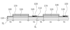
도 3은 본 발명의 일 실시예에 따른 유기발광 소자의 구조를 도시하는 단면도이다.
도 4 내지 도 11은 본 발명의 일 실시예에 따른 유기발광 소자 제조방법의 공정을 도시하는 도면들이다.
110 : 기판 120 : 유기 발광 구조물
130 : 게이트 라인 140 : 데이터 라인
150 : FPC 연결 패드 160, 170, 180 : 제1, 2, 3 무기봉지 박막
190 : 보호막 112 : 베리어층
Claims (9)
- 액티브 영역과 비액티브 영역으로 정의된 다수개의 셀 영역이 스크라이빙 라인에 의하여 구분되어 있는 플렉서블(flexible)한 기판;
상기 기판 상부 중 액티브 영역에 형성된 유기 발광 구조물;
상기 유기 발광 구조물을 구동시키기 위하여 상기 액티브 영역과 비액티브 영역에 걸쳐서 형성되는 게이트 라인 및 데이터 라인;
상기 기판 상부 중 비액티브 영역에 형성되며, 상기 게이트 라인 및 데이터 라인의 말단들과 연결되는 FPC 연결 패드;
상기 기판 전면 중 상기 FPC 연결 패드 상부를 제외한 제1 형성영역에 형성되는 제1 무기 봉지 박막;
상기 제1 무기 봉지박막이 형성된 기판 중 액티브 영역과 비액티브 영역의 일부분을 포함하는 제2 형성영역에 형성되는 제2 무기 봉지 박막;
상기 제1, 2 무기 봉지 박막이 형성된 기판 상면 중 상기 제1 형성 영역과 동일한 영역에 형성되는 제3 무기 봉지 박막;
상기 제3 무기 봉지 박막이 형성된 기판 상면 중 제1 형성 영역과 동일한 영역에 형성되는 보호막;을 포함하는 유기 발광 소자. - 제1항에 있어서,
상기 제1, 3 무기 봉지 박막은 산화알루미늄(Al2O3)인 것을 특징으로 하는 유기 발광 소자. - 제2항에 있어서,
상기 제2 무기 봉지 박막과 보호막은 실리콘 산화 질화물(SiON)인 것을 특징으로 하는 유기 발광 소자. - 제1항에 있어서,
상기 기판 상면에는 베리어층이 더 형성되는 것을 특징으로 하는 유기 발광 소자. - 제5항에 있어서, 상기 베리어층은,
산화알루미늄(Al2O3)인 것을 특징으로 하는 유기 발광 소자. - 1) 액티브 영역과 비액티브 영역으로 정의된 다수개의 셀 영역이 스크라이빙 라인에 의하여 구분되어 있는 플렉서블한 기판 중 상기 액티브 영역에 유기 발광 구조물을 형성하고, 상기 액티브 영역과 비액티브 영역에 걸쳐서 상기 유기 발광 구조물을 구동하기 위한 게이트 라인 및 데이터 라인을 형성하고, 상기 게이트 라인 및 데이터 라인의 말단들과 연결되는 FPC 연결 패드를 상기 비액티브 영역에 형성하여 유기발광 기판을 제조하는 단계;
2) 상기 유기발광 기판의 전면에 제1 무기 봉지 박막을 형성하는 단계;
3) 상기 제1 무기 봉지 박막이 형성된 기판 상면 중 액티브 영역과 비액티브 영역의 일부분을 포함하는 제2 형성영역에 제2 무기 봉지 박막을 형성하는 단계;
4) 상기 제2 무기 봉지 박막이 형성된 기판 전면에 제3 무기 봉지 박막을 형성하는 단계;
5) 상기 제3 무기 봉지 박막이 형성된 기판 중 상기 FPC 패드 형성 상면을 포함하는 식각 영역을 제외한 영역에 보호막을 형성하는 단계;
6) 상기 제1, 3 무기 봉지 박막 중 상기 보호막에 의하여 개방되어 있는 부분을 식각하여 제거하는 단계;를 포함하는 유기 발광 소자 제조방법. - 제6항에 있어서, 상기 2), 4) 단계에서는,
상기 제1, 3 무기 봉지 박막으로 산화알루미늄(Al2O3)을 원자층 증착 방법으로 형성하는 것을 특징으로 하는 유기발광 소자 제조방법. - 제7항에 있어서, 상기 3), 5) 단계에서는,
상기 제2 무기 봉지 박막과 보호막으로 실리콘 산화 질화물(SiON)을 화학기상증착 방법으로 증착하는 것을 특징으로 하는 유기발광 소자 제조방법. - 제8항에 있어서, 상기 6) 단계에서는,
상기 보호막을 마스크로 사용하여 상기 제1, 3 무기 봉지 박막을 건식 식각하는 것을 특징으로 하는 유기발광 소자 제조방법.
Priority Applications (1)
| Application Number | Priority Date | Filing Date | Title |
|---|---|---|---|
| KR1020140157017A KR101676764B1 (ko) | 2014-11-12 | 2014-11-12 | 유기발광 소자 및 이의 제조방법 |
Applications Claiming Priority (1)
| Application Number | Priority Date | Filing Date | Title |
|---|---|---|---|
| KR1020140157017A KR101676764B1 (ko) | 2014-11-12 | 2014-11-12 | 유기발광 소자 및 이의 제조방법 |
Publications (2)
| Publication Number | Publication Date |
|---|---|
| KR20160056581A true KR20160056581A (ko) | 2016-05-20 |
| KR101676764B1 KR101676764B1 (ko) | 2016-11-17 |
Family
ID=56103726
Family Applications (1)
| Application Number | Title | Priority Date | Filing Date |
|---|---|---|---|
| KR1020140157017A Active KR101676764B1 (ko) | 2014-11-12 | 2014-11-12 | 유기발광 소자 및 이의 제조방법 |
Country Status (1)
| Country | Link |
|---|---|
| KR (1) | KR101676764B1 (ko) |
Cited By (4)
| Publication number | Priority date | Publication date | Assignee | Title |
|---|---|---|---|---|
| CN111192865A (zh) * | 2020-03-05 | 2020-05-22 | 江苏壹光科技有限公司 | 一种双面发光无引线oled模组 |
| KR102165742B1 (ko) * | 2019-04-04 | 2020-10-14 | 주식회사 엔씨디 | 유기발광 표시장치 및 제조방법 |
| KR102183409B1 (ko) * | 2020-05-18 | 2020-11-26 | 주식회사 엔씨디 | 박막 인캡 상에 터치스크린 패널을 형성하는 방법 |
| CN113675356A (zh) * | 2020-05-14 | 2021-11-19 | Ncd有限公司 | 在薄膜封装体上形成触摸屏板的方法 |
Families Citing this family (2)
| Publication number | Priority date | Publication date | Assignee | Title |
|---|---|---|---|---|
| JP2023528076A (ja) * | 2020-06-08 | 2023-07-03 | ソウル バイオシス カンパニー リミテッド | 発光素子を有するユニットピクセル及びディスプレイ装置 |
| US12364073B2 (en) | 2020-06-08 | 2025-07-15 | Seoul Viosys Co., Ltd. | Unit pixel having light emitting device and displaying apparatus |
Citations (4)
| Publication number | Priority date | Publication date | Assignee | Title |
|---|---|---|---|---|
| KR20100119557A (ko) * | 2008-01-30 | 2010-11-09 | 오스람 옵토 세미컨덕터스 게엠베하 | 밀봉 유닛을 포함한 장치 |
| KR20110049341A (ko) * | 2009-11-05 | 2011-05-12 | 엘지디스플레이 주식회사 | 유기발광 표시장치의 제조방법 및 이에 이용되는 유기발광 표시 기판 |
| KR20110096755A (ko) * | 2010-02-23 | 2011-08-31 | 엘지디스플레이 주식회사 | 유기 발광 표시 장치 및 이의 제조 방법 |
| KR20140062376A (ko) * | 2012-11-14 | 2014-05-23 | 삼성디스플레이 주식회사 | 유기 발광 디스플레이 장치 |
-
2014
- 2014-11-12 KR KR1020140157017A patent/KR101676764B1/ko active Active
Patent Citations (4)
| Publication number | Priority date | Publication date | Assignee | Title |
|---|---|---|---|---|
| KR20100119557A (ko) * | 2008-01-30 | 2010-11-09 | 오스람 옵토 세미컨덕터스 게엠베하 | 밀봉 유닛을 포함한 장치 |
| KR20110049341A (ko) * | 2009-11-05 | 2011-05-12 | 엘지디스플레이 주식회사 | 유기발광 표시장치의 제조방법 및 이에 이용되는 유기발광 표시 기판 |
| KR20110096755A (ko) * | 2010-02-23 | 2011-08-31 | 엘지디스플레이 주식회사 | 유기 발광 표시 장치 및 이의 제조 방법 |
| KR20140062376A (ko) * | 2012-11-14 | 2014-05-23 | 삼성디스플레이 주식회사 | 유기 발광 디스플레이 장치 |
Cited By (6)
| Publication number | Priority date | Publication date | Assignee | Title |
|---|---|---|---|---|
| KR102165742B1 (ko) * | 2019-04-04 | 2020-10-14 | 주식회사 엔씨디 | 유기발광 표시장치 및 제조방법 |
| CN111785753A (zh) * | 2019-04-04 | 2020-10-16 | Ncd株式会社 | 有机发光显示装置及制造方法 |
| CN111785753B (zh) * | 2019-04-04 | 2023-12-08 | Ncd株式会社 | 有机发光显示装置及制造方法 |
| CN111192865A (zh) * | 2020-03-05 | 2020-05-22 | 江苏壹光科技有限公司 | 一种双面发光无引线oled模组 |
| CN113675356A (zh) * | 2020-05-14 | 2021-11-19 | Ncd有限公司 | 在薄膜封装体上形成触摸屏板的方法 |
| KR102183409B1 (ko) * | 2020-05-18 | 2020-11-26 | 주식회사 엔씨디 | 박막 인캡 상에 터치스크린 패널을 형성하는 방법 |
Also Published As
| Publication number | Publication date |
|---|---|
| KR101676764B1 (ko) | 2016-11-17 |
Similar Documents
| Publication | Publication Date | Title |
|---|---|---|
| KR100873704B1 (ko) | 유기 전계 발광표시장치 및 그의 제조방법 | |
| US20200274101A1 (en) | Display device | |
| KR101927334B1 (ko) | 유기전계발광소자 및 그 제조방법 | |
| KR101676764B1 (ko) | 유기발광 소자 및 이의 제조방법 | |
| JP2005317476A (ja) | 表示装置 | |
| KR102062912B1 (ko) | 유기발광 다이오드 표시장치 및 그 제조 방법 | |
| WO2016163367A1 (ja) | El表示装置およびel表示装置の製造方法 | |
| CN108428728A (zh) | 阵列基板及制作方法、显示面板及制作方法、显示装置 | |
| JP6837410B2 (ja) | 発光領域を含むディスプレイ装置 | |
| KR20150033345A (ko) | 유기발광 다이오드 표시장치 및 그 제조 방법 | |
| US20150125666A1 (en) | Display device and method of manufacturing the same | |
| WO2006064715A1 (ja) | 表示装置及び表示装置の製造方法 | |
| JP2006004650A (ja) | 表示素子及び光学デバイス | |
| KR101379650B1 (ko) | 쉐도우 마스크, 이로 제조된 유기전계발광표시장치 및 그제조방법 | |
| KR100685841B1 (ko) | 유기 전계 발광 표시 장치 및 그의 제조 방법 | |
| KR101950837B1 (ko) | 유기전계발광소자 및 그 제조방법 | |
| KR100360328B1 (ko) | 유기 전계발광 표시소자 | |
| KR102034050B1 (ko) | 플렉서블 유기발광 표시장치 | |
| JP2005353398A (ja) | 表示素子、光学デバイス、及び光学デバイスの製造方法 | |
| KR102799538B1 (ko) | 유기 발광 표시 장치 및 그의 제조 방법 | |
| KR101818470B1 (ko) | 유기 발광 표시 장치 및 이의 제조 방법 | |
| KR102361967B1 (ko) | 유기전계발광 표시장치 | |
| KR100417921B1 (ko) | 캔리스 유기 전계 발광 디스플레이 | |
| KR100658341B1 (ko) | 전계발광소자 및 그 제조방법 | |
| KR102183409B1 (ko) | 박막 인캡 상에 터치스크린 패널을 형성하는 방법 |
Legal Events
| Date | Code | Title | Description |
|---|---|---|---|
| A201 | Request for examination | ||
| PA0109 | Patent application |
St.27 status event code: A-0-1-A10-A12-nap-PA0109 |
|
| PA0201 | Request for examination |
St.27 status event code: A-1-2-D10-D11-exm-PA0201 |
|
| E902 | Notification of reason for refusal | ||
| PE0902 | Notice of grounds for rejection |
St.27 status event code: A-1-2-D10-D21-exm-PE0902 |
|
| AMND | Amendment | ||
| E13-X000 | Pre-grant limitation requested |
St.27 status event code: A-2-3-E10-E13-lim-X000 |
|
| P11-X000 | Amendment of application requested |
St.27 status event code: A-2-2-P10-P11-nap-X000 |
|
| P13-X000 | Application amended |
St.27 status event code: A-2-2-P10-P13-nap-X000 |
|
| E902 | Notification of reason for refusal | ||
| PE0902 | Notice of grounds for rejection |
St.27 status event code: A-1-2-D10-D21-exm-PE0902 |
|
| T11-X000 | Administrative time limit extension requested |
St.27 status event code: U-3-3-T10-T11-oth-X000 |
|
| T11-X000 | Administrative time limit extension requested |
St.27 status event code: U-3-3-T10-T11-oth-X000 |
|
| PG1501 | Laying open of application |
St.27 status event code: A-1-1-Q10-Q12-nap-PG1501 |
|
| AMND | Amendment | ||
| P11-X000 | Amendment of application requested |
St.27 status event code: A-2-2-P10-P11-nap-X000 |
|
| P13-X000 | Application amended |
St.27 status event code: A-2-2-P10-P13-nap-X000 |
|
| E601 | Decision to refuse application | ||
| PE0601 | Decision on rejection of patent |
St.27 status event code: N-2-6-B10-B15-exm-PE0601 |
|
| AMND | Amendment | ||
| P11-X000 | Amendment of application requested |
St.27 status event code: A-2-2-P10-P11-nap-X000 |
|
| P13-X000 | Application amended |
St.27 status event code: A-2-2-P10-P13-nap-X000 |
|
| PX0901 | Re-examination |
St.27 status event code: A-2-3-E10-E12-rex-PX0901 |
|
| PX0701 | Decision of registration after re-examination |
St.27 status event code: A-3-4-F10-F13-rex-PX0701 |
|
| X701 | Decision to grant (after re-examination) | ||
| GRNT | Written decision to grant | ||
| PR0701 | Registration of establishment |
St.27 status event code: A-2-4-F10-F11-exm-PR0701 |
|
| PR1002 | Payment of registration fee |
St.27 status event code: A-2-2-U10-U11-oth-PR1002 Fee payment year number: 1 |
|
| PG1601 | Publication of registration |
St.27 status event code: A-4-4-Q10-Q13-nap-PG1601 |
|
| PR1001 | Payment of annual fee |
St.27 status event code: A-4-4-U10-U11-oth-PR1001 Fee payment year number: 4 |
|
| PR1001 | Payment of annual fee |
St.27 status event code: A-4-4-U10-U11-oth-PR1001 Fee payment year number: 5 |
|
| PR1001 | Payment of annual fee |
St.27 status event code: A-4-4-U10-U11-oth-PR1001 Fee payment year number: 6 |
|
| PR1001 | Payment of annual fee |
St.27 status event code: A-4-4-U10-U11-oth-PR1001 Fee payment year number: 7 |
|
| P22-X000 | Classification modified |
St.27 status event code: A-4-4-P10-P22-nap-X000 |
|
| P22-X000 | Classification modified |
St.27 status event code: A-4-4-P10-P22-nap-X000 |
|
| PR1001 | Payment of annual fee |
St.27 status event code: A-4-4-U10-U11-oth-PR1001 Fee payment year number: 8 |
|
| PR1001 | Payment of annual fee |
St.27 status event code: A-4-4-U10-U11-oth-PR1001 Fee payment year number: 9 |
|
| P22-X000 | Classification modified |
St.27 status event code: A-4-4-P10-P22-nap-X000 |
|
| PR1001 | Payment of annual fee |
St.27 status event code: A-4-4-U10-U11-oth-PR1001 Fee payment year number: 10 |
|
| U11 | Full renewal or maintenance fee paid |
Free format text: ST27 STATUS EVENT CODE: A-4-4-U10-U11-OTH-PR1001 (AS PROVIDED BY THE NATIONAL OFFICE) Year of fee payment: 10 |