KR20160077196A - Resonant type high frequency power supply device - Google Patents
Resonant type high frequency power supply device Download PDFInfo
- Publication number
- KR20160077196A KR20160077196A KR1020167014462A KR20167014462A KR20160077196A KR 20160077196 A KR20160077196 A KR 20160077196A KR 1020167014462 A KR1020167014462 A KR 1020167014462A KR 20167014462 A KR20167014462 A KR 20167014462A KR 20160077196 A KR20160077196 A KR 20160077196A
- Authority
- KR
- South Korea
- Prior art keywords
- resonance
- high frequency
- condition
- power supply
- circuit element
- Prior art date
- Legal status (The legal status is an assumption and is not a legal conclusion. Google has not performed a legal analysis and makes no representation as to the accuracy of the status listed.)
- Withdrawn
Links
Images



Classifications
-
- H—ELECTRICITY
- H02—GENERATION; CONVERSION OR DISTRIBUTION OF ELECTRIC POWER
- H02M—APPARATUS FOR CONVERSION BETWEEN AC AND AC, BETWEEN AC AND DC, OR BETWEEN DC AND DC, AND FOR USE WITH MAINS OR SIMILAR POWER SUPPLY SYSTEMS; CONVERSION OF DC OR AC INPUT POWER INTO SURGE OUTPUT POWER; CONTROL OR REGULATION THEREOF
- H02M7/00—Conversion of AC power input into DC power output; Conversion of DC power input into AC power output
- H02M7/42—Conversion of DC power input into AC power output without possibility of reversal
- H02M7/44—Conversion of DC power input into AC power output without possibility of reversal by static converters
- H02M7/48—Conversion of DC power input into AC power output without possibility of reversal by static converters using discharge tubes with control electrode or semiconductor devices with control electrode
- H02M7/53—Conversion of DC power input into AC power output without possibility of reversal by static converters using discharge tubes with control electrode or semiconductor devices with control electrode using devices of a triode or transistor type requiring continuous application of a control signal
- H02M7/533—Conversion of DC power input into AC power output without possibility of reversal by static converters using discharge tubes with control electrode or semiconductor devices with control electrode using devices of a triode or transistor type requiring continuous application of a control signal using discharge tubes only
-
- H—ELECTRICITY
- H02—GENERATION; CONVERSION OR DISTRIBUTION OF ELECTRIC POWER
- H02M—APPARATUS FOR CONVERSION BETWEEN AC AND AC, BETWEEN AC AND DC, OR BETWEEN DC AND DC, AND FOR USE WITH MAINS OR SIMILAR POWER SUPPLY SYSTEMS; CONVERSION OF DC OR AC INPUT POWER INTO SURGE OUTPUT POWER; CONTROL OR REGULATION THEREOF
- H02M7/00—Conversion of AC power input into DC power output; Conversion of DC power input into AC power output
- H02M7/42—Conversion of DC power input into AC power output without possibility of reversal
- H02M7/44—Conversion of DC power input into AC power output without possibility of reversal by static converters
- H02M7/48—Conversion of DC power input into AC power output without possibility of reversal by static converters using discharge tubes with control electrode or semiconductor devices with control electrode
- H02M7/53—Conversion of DC power input into AC power output without possibility of reversal by static converters using discharge tubes with control electrode or semiconductor devices with control electrode using devices of a triode or transistor type requiring continuous application of a control signal
- H02M7/537—Conversion of DC power input into AC power output without possibility of reversal by static converters using discharge tubes with control electrode or semiconductor devices with control electrode using devices of a triode or transistor type requiring continuous application of a control signal using semiconductor devices only, e.g. single switched pulse inverters
- H02M7/5383—Conversion of DC power input into AC power output without possibility of reversal by static converters using discharge tubes with control electrode or semiconductor devices with control electrode using devices of a triode or transistor type requiring continuous application of a control signal using semiconductor devices only, e.g. single switched pulse inverters in a self-oscillating arrangement
- H02M7/53832—Conversion of DC power input into AC power output without possibility of reversal by static converters using discharge tubes with control electrode or semiconductor devices with control electrode using devices of a triode or transistor type requiring continuous application of a control signal using semiconductor devices only, e.g. single switched pulse inverters in a self-oscillating arrangement in a push-pull arrangement
-
- H—ELECTRICITY
- H02—GENERATION; CONVERSION OR DISTRIBUTION OF ELECTRIC POWER
- H02J—ELECTRIC POWER NETWORKS; CIRCUIT ARRANGEMENTS OR SYSTEMS FOR SUPPLYING OR DISTRIBUTING ELECTRIC POWER; SYSTEMS FOR STORING ELECTRIC ENERGY
- H02J50/00—Circuit arrangements or systems for wireless supply or distribution of electric power
- H02J50/10—Circuit arrangements or systems for wireless supply or distribution of electric power using inductive coupling
- H02J50/12—Circuit arrangements or systems for wireless supply or distribution of electric power using inductive coupling of the resonant type
-
- H—ELECTRICITY
- H02—GENERATION; CONVERSION OR DISTRIBUTION OF ELECTRIC POWER
- H02M—APPARATUS FOR CONVERSION BETWEEN AC AND AC, BETWEEN AC AND DC, OR BETWEEN DC AND DC, AND FOR USE WITH MAINS OR SIMILAR POWER SUPPLY SYSTEMS; CONVERSION OF DC OR AC INPUT POWER INTO SURGE OUTPUT POWER; CONTROL OR REGULATION THEREOF
- H02M1/00—Details of apparatus for conversion
- H02M1/0048—Circuits or arrangements for reducing losses
- H02M1/0054—Transistor switching losses
- H02M1/0058—Transistor switching losses by employing soft switching techniques, i.e. commutation of transistors when applied voltage is zero or when current flow is zero
-
- H—ELECTRICITY
- H02—GENERATION; CONVERSION OR DISTRIBUTION OF ELECTRIC POWER
- H02M—APPARATUS FOR CONVERSION BETWEEN AC AND AC, BETWEEN AC AND DC, OR BETWEEN DC AND DC, AND FOR USE WITH MAINS OR SIMILAR POWER SUPPLY SYSTEMS; CONVERSION OF DC OR AC INPUT POWER INTO SURGE OUTPUT POWER; CONTROL OR REGULATION THEREOF
- H02M7/00—Conversion of AC power input into DC power output; Conversion of DC power input into AC power output
- H02M7/42—Conversion of DC power input into AC power output without possibility of reversal
- H02M7/44—Conversion of DC power input into AC power output without possibility of reversal by static converters
- H02M7/48—Conversion of DC power input into AC power output without possibility of reversal by static converters using discharge tubes with control electrode or semiconductor devices with control electrode
-
- H—ELECTRICITY
- H02—GENERATION; CONVERSION OR DISTRIBUTION OF ELECTRIC POWER
- H02M—APPARATUS FOR CONVERSION BETWEEN AC AND AC, BETWEEN AC AND DC, OR BETWEEN DC AND DC, AND FOR USE WITH MAINS OR SIMILAR POWER SUPPLY SYSTEMS; CONVERSION OF DC OR AC INPUT POWER INTO SURGE OUTPUT POWER; CONTROL OR REGULATION THEREOF
- H02M7/00—Conversion of AC power input into DC power output; Conversion of DC power input into AC power output
- H02M7/42—Conversion of DC power input into AC power output without possibility of reversal
- H02M7/44—Conversion of DC power input into AC power output without possibility of reversal by static converters
- H02M7/48—Conversion of DC power input into AC power output without possibility of reversal by static converters using discharge tubes with control electrode or semiconductor devices with control electrode
- H02M7/4815—Resonant converters
-
- H—ELECTRICITY
- H02—GENERATION; CONVERSION OR DISTRIBUTION OF ELECTRIC POWER
- H02M—APPARATUS FOR CONVERSION BETWEEN AC AND AC, BETWEEN AC AND DC, OR BETWEEN DC AND DC, AND FOR USE WITH MAINS OR SIMILAR POWER SUPPLY SYSTEMS; CONVERSION OF DC OR AC INPUT POWER INTO SURGE OUTPUT POWER; CONTROL OR REGULATION THEREOF
- H02M7/00—Conversion of AC power input into DC power output; Conversion of DC power input into AC power output
- H02M7/42—Conversion of DC power input into AC power output without possibility of reversal
- H02M7/44—Conversion of DC power input into AC power output without possibility of reversal by static converters
- H02M7/48—Conversion of DC power input into AC power output without possibility of reversal by static converters using discharge tubes with control electrode or semiconductor devices with control electrode
- H02M7/4815—Resonant converters
- H02M7/4818—Resonant converters with means for adaptation of resonance frequency, e.g. by modification of capacitance or inductance of resonance circuits
-
- H—ELECTRICITY
- H03—ELECTRONIC CIRCUITRY
- H03H—IMPEDANCE NETWORKS, e.g. RESONANT CIRCUITS; RESONATORS
- H03H7/00—Multiple-port networks comprising only passive electrical elements as network components
- H03H7/38—Impedance-matching networks
-
- H—ELECTRICITY
- H02—GENERATION; CONVERSION OR DISTRIBUTION OF ELECTRIC POWER
- H02J—ELECTRIC POWER NETWORKS; CIRCUIT ARRANGEMENTS OR SYSTEMS FOR SUPPLYING OR DISTRIBUTING ELECTRIC POWER; SYSTEMS FOR STORING ELECTRIC ENERGY
- H02J50/00—Circuit arrangements or systems for wireless supply or distribution of electric power
- H02J50/05—Circuit arrangements or systems for wireless supply or distribution of electric power using capacitive coupling
-
- H02M2001/0058—
-
- H02M2007/4815—
-
- H02M2007/4818—
-
- Y—GENERAL TAGGING OF NEW TECHNOLOGICAL DEVELOPMENTS; GENERAL TAGGING OF CROSS-SECTIONAL TECHNOLOGIES SPANNING OVER SEVERAL SECTIONS OF THE IPC; TECHNICAL SUBJECTS COVERED BY FORMER USPC CROSS-REFERENCE ART COLLECTIONS [XRACs] AND DIGESTS
- Y02—TECHNOLOGIES OR APPLICATIONS FOR MITIGATION OR ADAPTATION AGAINST CLIMATE CHANGE
- Y02B—CLIMATE CHANGE MITIGATION TECHNOLOGIES RELATED TO BUILDINGS, e.g. HOUSING, HOUSE APPLIANCES OR RELATED END-USER APPLICATIONS
- Y02B70/00—Technologies for an efficient end-user side electric power management and consumption
- Y02B70/10—Technologies improving the efficiency by using switched-mode power supplies [SMPS], i.e. efficient power electronics conversion e.g. power factor correction or reduction of losses in power supplies or efficient standby modes
-
- Y02B70/1441—
-
- Y02B70/1491—
Landscapes
- Engineering & Computer Science (AREA)
- Power Engineering (AREA)
- Computer Networks & Wireless Communication (AREA)
- Dc-Dc Converters (AREA)
- Electronic Switches (AREA)
- Transmitters (AREA)
Abstract
2㎒를 넘는 고주파수의 스위칭 동작을 행하는 파워 소자를 구비한 공진형 고주파 전원 장치로서, 파워 소자의 스위칭 전압 공진 레벨 조정 및 출력 전압의 파형 제어를 행하는 공진 정합 필터(4)를 구비했다.A resonance type high frequency power supply device including a power device for performing a switching operation of a high frequency exceeding 2 MHz is provided with a resonance matching filter 4 for adjusting the switching voltage resonance level of the power device and controlling the waveform of the output voltage.

Description
본 발명은, 고주파수로 전력 전송을 행하는 공진형 고주파 전원 장치에 관한 것이다.BACKGROUND OF THE
도 8에 나타내는 종래의 공진형 고주파 전원 장치에서는, 파워 소자(FET)(101)의 드레인ㆍ소스 사이에 병렬 접속한 인덕터(102) 및 커패시터(103)에 의해, FET(101)의 기생 용량(104)이 큰 경우에도 FET(101)의 공진 스위칭의 조건을 유지할 수 있도록 구성하고 있다(예컨대 특허 문헌 1 참조).In the conventional resonance type high frequency power supply apparatus shown in Fig. 8, the parasitic capacitance (the parasitic capacitance) of the FET 101 is set by the
(선행 기술 문헌)(Prior art document)
(특허 문헌)(Patent Literature)
(특허 문헌 1) 일본 특허 공개 2013-30973호 공보(Patent Document 1) JP-A-2013-30973
그렇지만, 특허 문헌 1에 개시된 종래 기술에서는, FET(101)의 기생 용량(104)에 대하여 공진 스위칭의 조건을 유지할 수 있도록 설정하고 있기 때문에, 출력에 연결되는 부하의 임피던스 변동에 대해서는 보상할 수 없다. 따라서, 부하로서 와이어리스 전력 전송용 안테나 등, 공진 조건을 갖는 임피던스 소자가 접근하거나 멀어지거나 하면, 공진 스위칭의 조건이 무너져 버린다고 하는 과제가 있다. 그리고, 공진 스위칭의 조건이 무너지면 FET 등의 전력 손실이 급격하게 증가하기 때문에, 그 대책을 위한 배열 장치를 구비할 필요가 있다. 또한, 종래 기술에서는, 출력 전압의 파형 제어에 대해서도 고려되고 있지 않고, 전력 전송의 고효율화를 도모할 수 없다고 하는 과제도 있다.However, in the prior art disclosed in
본 발명은, 상기와 같은 과제를 해결하기 위해 이루어진 것으로, 부하의 임피던스 변동에 대하여 공진 스위칭의 조건을 유지하고, 또한 출력 전압의 파형 제어를 행할 수 있고, 2㎒를 넘는 고주파수의 동작이 가능한 공진형 고주파 전원 장치를 제공하는 것을 목적으로 하고 있다.SUMMARY OF THE INVENTION The present invention has been made to solve the above-mentioned problems, and it is an object of the present invention to provide a resonance circuit capable of maintaining the conditions of resonance switching with respect to impedance variation of a load, Type high-frequency power supply device.
본 발명과 관련되는 공진형 고주파 전원 장치는, 2㎒를 넘는 고주파수의 스위칭 동작을 행하는 파워 소자를 구비한 공진형 고주파 전원 장치로서, 파워 소자의 스위칭 전압 및 장치 출력 전압의 파형 제어를 행하는 공진 정합 필터를 구비한 것이다.The resonance type high frequency power supply apparatus according to the present invention is a resonance type high frequency power supply apparatus including a power element for performing a switching operation at a high frequency exceeding 2 MHz and includes a resonance matching Filter.
본 발명에 의하면, 상기와 같이 구성했으므로, 부하의 임피던스 변동에 대하여 공진 스위칭의 조건을 유지하고, 또한 출력 전압의 파형 제어를 행할 수 있고, 2㎒를 넘는 고주파수의 동작이 가능하게 된다.According to the present invention, the resonance switching condition can be maintained with respect to the impedance variation of the load, waveform control of the output voltage can be performed, and operation at a high frequency exceeding 2 MHz becomes possible.
도 1은 본 발명의 실시의 형태 1과 관련되는 공진형 고주파 전원 장치의 구성을 나타내는 도면이다(파워 소자가 싱글 구성).
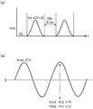
도 2는 본 발명의 실시의 형태 1과 관련되는 공진형 고주파 전원 장치의 Vds 파형과 Vout 파형을 나타내는 도면이다.
도 3은 본 발명의 실시의 형태 1과 관련되는 공진형 고주파 전원 장치의 다른 구성을 나타내는 도면이다.
도 4는 본 발명의 실시의 형태 1과 관련되는 공진형 고주파 전원 장치의 다른 구성을 나타내는 도면이다.
도 5는 본 발명의 실시의 형태 1과 관련되는 공진형 고주파 전원 장치의 다른 구성을 나타내는 도면이다(파워 소자가 푸시풀 구성).
도 6은 본 발명의 실시의 형태 1과 관련되는 공진형 고주파 전원 장치의 다른 구성을 나타내는 도면이다(공진 조건 가변형 공진 정합 필터를 마련한 경우).
도 7은 본 발명의 실시의 형태 1과 관련되는 공진형 고주파 전원 장치의 다른 구성을 나타내는 도면이다(공진 조건 가변 회로를 마련한 경우).
도 8은 종래의 공진형 고주파 전원 장치의 구성을 나타내는 도면이다.1 is a diagram showing a configuration of a resonance type high frequency power source device according to a first embodiment of the present invention (a power element has a single configuration).
2 is a diagram showing the Vds waveform and the Vout waveform of the resonance type high frequency power supply device according to the first embodiment of the present invention.
3 is a diagram showing another configuration of a resonance type high frequency power supply device according to
4 is a diagram showing another configuration of a resonance type high frequency power supply device according to
5 is a diagram showing another configuration of a resonance type high frequency power supply device according to
6 is a diagram showing another configuration of a resonance type high frequency power supply device according to
7 is a diagram showing another configuration of a resonance type high frequency power supply device according to
8 is a diagram showing a configuration of a conventional resonance type high frequency power supply device.
이하, 본 발명의 실시의 형태에 대하여 도면을 참조하면서 상세하게 설명한다.DESCRIPTION OF THE PREFERRED EMBODIMENTS Hereinafter, embodiments of the present invention will be described in detail with reference to the drawings.
실시의 형태 1.
도 1은 본 발명의 실시의 형태 1과 관련되는 공진형 고주파 전원 장치의 구성을 나타내는 도면이다. 또 도 1에서는, 파워 소자 Q1이 싱글 구성인 경우의 회로를 나타내고 있다.1 is a diagram showing a configuration of a resonance type high frequency power source device according to a first embodiment of the present invention. Fig. 1 shows a circuit in the case where the power device Q1 has a single configuration.
공진형 고주파 전원 장치는, 도 1에 나타내는 바와 같이, 파워 소자 Q1, 공진 회로 소자(콘덴서 C1, C2 및 인덕터 L2), 인덕터 L1, 고주파 펄스 드라이브 회로(1), 가변형 펄스 신호 발생 회로(2), 바이어스용 전원 회로(3) 및 공진 정합 필터(4)로 구성되어 있다.1, the resonance type high frequency power supply device includes a power device Q1, resonance circuit elements (capacitors C1 and C2 and an inductor L2), an inductor L1, a high frequency
또, 공진형 송신 안테나(전력 전송용 송신 안테나)(10)는, LC 공진 특성을 갖는 전력 전송용 공진형 안테나이다(비접촉형으로만 한정되지 않는다). 이 공진형 송신 안테나(10)는, 자계 공명형, 전계 공명형, 전자기 유도형 중 어느 것이더라도 좋다.The resonance type transmission antenna (power transmission transmission antenna) 10 is a power transmission resonance type antenna having LC resonance characteristics (it is not limited to a non-contact type). The resonance
파워 소자 Q1은, 입력의 직류 전압 Vin을 교류로 변환하기 위해 스위칭 동작을 행하는 스위칭 소자이다. 이 파워 소자 Q1로서는, RF용 FET에 한하지 않고, 예컨대 Si-MOSFET나 SiC-MOSFET, GaN-FET 등의 소자를 이용하는 것이 가능하다.The power device Q1 is a switching device that performs a switching operation to convert an input DC voltage Vin into AC. The power device Q1 is not limited to the RF-use FET, and for example, an element such as a Si-MOSFET, a SiC-MOSFET, or a GaN-FET can be used.
공진 회로 소자(콘덴서 C1, C2 및 인덕터 L2)는, 파워 소자 Q1의 스위칭 동작을 공진 스위칭시키기 위한 소자이다. 이 콘덴서 C1, C2 및 인덕터 L2로 이루어지는 공진 회로 소자에 의해, 공진형 송신 안테나(10)와의 사이에서 공진 조건을 맞출 수 있다.The resonant circuit elements (capacitors C1 and C2 and inductor L2) are elements for resonantly switching the switching operation of the power device Q1. The resonance circuit element composed of the capacitors C1 and C2 and the inductor L2 can match the resonance condition with the resonance
인덕터 L1은, 입력의 직류 전압 Vin의 에너지를, 파워 소자 Q1의 스위칭 동작마다 일시적으로 유지하는 기능을 하는 것이다.The inductor L1 functions to temporarily hold the energy of the input DC voltage Vin for each switching operation of the power device Q1.
고주파 펄스 드라이브 회로(1)는, 파워 소자 Q1의 G 단자에 2㎒를 넘는 고주파수의 펄스 형상의 전압 신호를 보내서, 파워 소자 Q1을 구동시키는 회로이다. 이 고주파 펄스 드라이브 회로(1)는, 출력부를 FET 소자 등으로 토템폴 회로 구성으로 하여 고속의 ON/OFF 출력을 할 수 있도록 구성한 회로이다.The high-frequency
가변형 펄스 신호 발생 회로(2)는, 고주파 펄스 드라이브 회로(1)에 로직 신호 등의 2㎒를 넘는 고주파수의 펄스 형상의 전압 신호를 보내서, 고주파 펄스 드라이브 회로(1)를 구동시키는 회로이다. 이 가변형 펄스 신호 발생 회로(2)는, 주파수 설정용 오실레이터와 플립플롭이나 인버터 등의 로직 IC로 구성되고, 펄스 폭의 변경이나 반전 펄스 출력 등의 기능을 갖는다.The variable pulse
바이어스용 전원 회로(3)는, 가변형 펄스 신호 발생 회로(2) 및 고주파 펄스 드라이브 회로(1)로의 구동 전력의 공급을 행하는 것이다.The bias
공진 정합 필터(4)는, 파워 소자 Q1의 스위칭 전압 Vds 및 공진형 고주파 전원 장치의 출력 전압 Vout의 파형 제어를 행하는 것이다. 이것에 의해, 공진 회로 소자(콘덴서 C1, C2 및 인덕터 L2)의 출력 임피던스와 부하측의 공진형 송신 안테나(10)의 입력 임피던스의 정합을 취할 수 있다.The resonance matched
다음으로, 상기와 같이 구성된 공진형 고주파 전원 장치의 동작에 대하여 설명한다.Next, the operation of the resonance type high frequency power supply apparatus constructed as described above will be described.
우선, 입력의 직류 전압 Vin은 인덕터 L1을 통해서 파워 소자 Q1의 D 단자에 인가된다. 그리고, 파워 소자 Q1은, 그 전압을 ON/OFF의 스위칭 동작에 의해 정전압의 교류 형상 전압으로 변환한다. 이 변환 동작시에, 인덕터 L1은 일시적으로 에너지를 유지하는 기능을 하여, 직류를 교류로 전력 변환하는 것을 돕는다.First, the input DC voltage Vin is applied to the D terminal of the power device Q1 through the inductor L1. Then, the power device Q1 converts the voltage to a constant-voltage alternating-current voltage by the ON / OFF switching operation. In this conversion operation, the inductor L1 functions to temporarily hold the energy, thereby assisting in the power conversion of the direct current to the alternating current.
여기서, 파워 소자 Q1의 스위칭 동작은, Ids 전류와 Vds 전압의 곱에 의한 스위칭 손실이 가장 작아지도록, ZVS(제로 볼티지 스위칭)가 성립하도록 콘덴서 C1, C2 및 인덕터 L2로 이루어지는 공진 회로 소자에서 공진 스위칭 조건이 설정되어 있다. 이 공진 스위칭 동작에 의해, 출력 전압 Vout에는 RTN 전압을 축으로 한 교류 전압이 출력된다.Here, the switching operation of the power device Q1 is performed such that the switching loss due to the product of the Ids current and the Vds voltage becomes the smallest, and the ZVS (zero voltage switching) is established by resonance in the resonance circuit element composed of the capacitors C1 and C2 and the inductor L2 The switching conditions are set. By this resonance switching operation, an AC voltage having the RTN voltage as an axis is output to the output voltage Vout.
이때, 파워 소자 Q1의 스위칭 전압 Vds와 출력 전압 Vout의 관계는 공진 정합 필터(4)에 의해 설정되기 때문에, 부하측의 임피던스 변동에 의해 내부 회로의 공진 스위칭 조건이 변화하는 일은 없다. 또, 공진 정합 필터(4)의 정수는, Vds 및 Vout의 전압 파형이 도 2에 나타내는 바와 같은 조건에 맞도록 설정한다. 도 2(a)에 있어서, ON-Duty는 30~80%의 범위 내에서 동작한다.At this time, since the relationship between the switching voltage Vds of the power device Q1 and the output voltage Vout is set by the
파워 소자 Q1의 구동은, 가변형 펄스 신호 발생 회로(2)로부터의 임의의 펄스 형상의 전압 신호를 받은 고주파 펄스 드라이브 회로(1)가 출력하는, 펄스 형상의 전압 신호를 파워 소자 Q1의 G 단자에 입력하는 것에 의해 행하고 있다. 이때, 파워 소자 Q1의 구동 주파수는 공진형 고주파 전원 장치의 동작 주파수가 되고, 가변형 펄스 신호 발생 회로(2) 내부의 오실레이터 회로의 설정에 의해 정해진다.The driving of the power device Q1 is performed by supplying a pulse-shaped voltage signal, which is output from the high-frequency
이상과 같이, 본 실시의 형태 1에 의하면, 파워 소자 Q1의 스위칭 전압 Vds 및 출력 전압 Vout의 파형 제어를 행하는 공진 정합 필터(4)를 구비하도록 구성했으므로, 2㎒를 넘는 고주파수의 동작에 있어서, 부하의 임피던스 변동에 대하여 공진 스위칭의 조건을 유지하고(공진 스위칭의 조건을 50% 이상 무너뜨려 버리는 일이 없고), 또한 출력 전압 Vout의 파형 제어를 행할 수 있다.As described above, according to the first embodiment, since the
그 결과, 부하로서 와이어리스 전력 전송용 안테나 등, 공진 조건을 갖는 임피던스 소자가 접근하거나, 멀어지거나 하더라도, 급격한 전력 손실에 의한 발열을 일으키는 일은 없고, 발열 보호용 히트싱크 등의 배열 설계를 지나치게 행할 필요는 없다. 그 때문에, 비용의 삭감, 소형, 경량화 및 고효율화를 도모할 수 있다.As a result, even if an impedance element having a resonance condition such as an antenna for a wireless power transmission as a load approaches or moves away, there is no possibility of generating heat due to a sudden power loss, and it is not necessary to excessively design the heat- none. Therefore, the cost can be reduced, the size and weight can be reduced, and high efficiency can be achieved.
또 도 1에서는, 콘덴서 C3, C4로 이루어지는 공진 정합 필터(4)를 이용하는 경우에 대하여 나타냈지만, 이것에 한하는 것이 아니고, 예컨대 도 3, 4에 나타내는 바와 같은 구성의 공진 정합 필터(4)를 이용하더라도 좋다.1 shows the case where the resonance matched
또한 도 1에서는, 파워 소자 Q1을 구동시키기 위해, 고주파 펄스 드라이브 회로(1), 가변형 펄스 신호 발생 회로(2) 및 바이어스용 전원 회로(3)를 이용한 경우에 대하여 나타냈지만, 이것에 한하는 것이 아니고, 예컨대 트랜스형 드라이브 회로, RF 파워 앰프 회로 및 다출력형 전원 회로를 이용하도록 하더라도 좋다.1 shows a case where the high-frequency
또한 도 1에서는, 파워 소자 Q1이 싱글 구성인 경우의 회로에 대하여 나타냈지만, 이것에 한하는 것이 아니고, 예컨대 도 5에 나타내는 바와 같이, 파워 소자 Q1이 푸시풀 구성인 경우에도 마찬가지로 본 발명을 적용 가능하다.1 shows a circuit in the case where the power device Q1 has a single configuration. However, the present invention is not limited thereto. For example, as shown in Fig. 5, when the power device Q1 has a push- It is possible.
또한 도 1에서는, 공진 회로 소자에 의한 공진 조건이 고정인 경우에 대하여 설명을 행했지만, 이것에 한하는 것이 아니고, 예컨대 도 6에 나타내는 바와 같이, 공진 회로 소자에 의한 공진 조건을 가변시키는 공진 조건 가변형 공진 정합 필터(5)를 이용하도록 하더라도 좋다. 또한, 예컨대 도 7에 나타내는 바와 같이, 상기 공진 회로 소자(콘덴서 C1, C2 및 인덕터 L2)에 의한 공진 조건을 가변시키는 공진 조건 가변 회로(6)를 별도로 마련하도록 하더라도 좋다.In Fig. 1, the case where the resonance condition by the resonance circuit element is fixed is described. However, as shown in Fig. 6, for example, a resonance condition for varying the resonance condition by the resonance circuit element The variable resonance matched
또한, 본원 발명은 그 발명의 범위 내에 있어서, 실시의 형태의 임의의 구성 요소의 변형, 또는 실시의 형태의 임의의 구성 요소의 생략이 가능하다.It is to be understood that the present invention may be embodied in other specific forms without departing from the spirit or essential characteristics thereof.
(산업상이용가능성)(Industrial applicability)
본 발명과 관련되는 공진형 고주파 전원 장치는, 부하의 임피던스 변동에 대하여 공진 스위칭의 조건을 유지하고, 또한 출력 전압의 파형 제어를 행할 수 있고, 2㎒를 넘는 고주파수의 동작이 가능하게 되고, 고주파수로 전력 전송을 행하는 공진형 고주파 전원 장치 등에 이용하는데 적합하다.The resonance type high frequency power supply device according to the present invention can maintain the resonance switching condition with respect to the impedance variation of the load and also can control the waveform of the output voltage and can operate at a high frequency exceeding 2 MHz, A resonance type high-frequency power supply device that performs power transmission to the resonance type high frequency power supply device, and the like.
1 : 고주파 펄스 드라이브 회로
2 : 가변형 펄스 신호 발생 회로
3 : 바이어스용 전원 회로
4 : 공진 정합 필터
5 : 공진 조건 가변형 공진 정합 필터
6 : 공진 조건 가변 회로
10 : 공진형 송신 안테나(전력 전송용 송신 안테나)1: High frequency pulse drive circuit
2: variable pulse signal generating circuit
3: Bias power supply circuit
4: Resonant matched filter
5: resonance condition variable resonance matched filter
6: Resonant condition variable circuit
10: Resonant transmission antenna (transmission antenna for power transmission)
Claims (12)
상기 파워 소자의 스위칭 전압 및 장치 출력 전압의 파형 제어를 행하는 공진 정합 필터를 구비한
것을 특징으로 하는 공진형 고주파 전원 장치.
A resonance type high frequency power supply device comprising a power device for performing a switching operation of a high frequency exceeding 2 MHz,
And a resonance matched filter for controlling the waveform of the switching voltage and the device output voltage of the power device
And the resonance type high frequency power supply device.
상기 파워 소자는, RF(Radio Frequency)용 FET(Field Effect Transistor) 이외의 FET인 것을 특징으로 하는 공진형 고주파 전원 장치.
The method according to claim 1,
Wherein the power device is an FET other than a RF (Field Frequency Transistor) FET (field effect transistor).
상기 파워 소자는, 푸시풀 구성 또는 싱글 구성인 것을 특징으로 하는 공진형 고주파 전원 장치.
The method according to claim 1,
Wherein the power device has a push-pull configuration or a single configuration.
자계 공명에 의한 전력 전송용 송신 안테나와의 사이에서 공진 조건을 맞추는 콘덴서 및 인덕터로 이루어지는 공진 회로 소자를 구비한 것을 특징으로 하는 공진형 고주파 전원 장치.
The method according to claim 1,
And a resonance circuit element composed of a capacitor and an inductor for matching the resonance condition with the transmission antenna for power transmission by magnetic field resonance.
전계 공명에 의한 전력 전송용 송신 안테나와의 사이에서 공진 조건을 맞추는 콘덴서 및 인덕터로 이루어지는 공진 회로 소자를 구비한 것을 특징으로 하는 공진형 고주파 전원 장치.
The method according to claim 1,
And a resonance circuit element composed of a capacitor and an inductor for matching the resonance condition with the transmission antenna for power transmission by electric field resonance.
전자기 유도에 의한 전력 전송용 송신 안테나와의 사이에서 공진 조건을 맞추는 콘덴서 및 인덕터로 이루어지는 공진 회로 소자를 구비한 것을 특징으로 하는 공진형 고주파 전원 장치.
The method according to claim 1,
And a resonance circuit element composed of a capacitor and an inductor for matching a resonance condition with a transmission antenna for power transmission by electromagnetic induction.
상기 공진 정합 필터는, 상기 공진 회로 소자의 공진 조건을 가변으로 하는 것을 특징으로 하는 공진형 고주파 전원 장치.5. The method of claim 4,
Wherein the resonance matching filter varies the resonance condition of the resonance circuit element.
상기 공진 정합 필터는, 상기 공진 회로 소자의 공진 조건을 가변으로 하는 것을 특징으로 하는 공진형 고주파 전원 장치.
6. The method of claim 5,
Wherein the resonance matching filter varies the resonance condition of the resonance circuit element.
상기 공진 정합 필터는, 상기 공진 회로 소자의 공진 조건을 가변으로 하는 것을 특징으로 하는 공진형 고주파 전원 장치.
The method according to claim 6,
Wherein the resonance matching filter varies the resonance condition of the resonance circuit element.
상기 공진 회로 소자의 공진 조건을 가변으로 하는 공진 조건 가변 회로를 구비한 것을 특징으로 하는 공진형 고주파 전원 장치.
5. The method of claim 4,
And a resonance condition variable circuit for varying a resonance condition of the resonance circuit element.
상기 공진 회로 소자의 공진 조건을 가변으로 하는 공진 조건 가변 회로를 구비한 것을 특징으로 하는 공진형 고주파 전원 장치.
6. The method of claim 5,
And a resonance condition variable circuit for varying a resonance condition of the resonance circuit element.
상기 공진 회로 소자의 공진 조건을 가변으로 하는 공진 조건 가변 회로를 구비한 것을 특징으로 하는 공진형 고주파 전원 장치.The method according to claim 6,
And a resonance condition variable circuit for varying a resonance condition of the resonance circuit element.
Applications Claiming Priority (1)
| Application Number | Priority Date | Filing Date | Title |
|---|---|---|---|
| PCT/JP2013/079552 WO2015063921A1 (en) | 2013-10-31 | 2013-10-31 | Resonant high frequency power source device |
Publications (1)
| Publication Number | Publication Date |
|---|---|
| KR20160077196A true KR20160077196A (en) | 2016-07-01 |
Family
ID=53003565
Family Applications (1)
| Application Number | Title | Priority Date | Filing Date |
|---|---|---|---|
| KR1020167014462A Withdrawn KR20160077196A (en) | 2013-10-31 | 2013-10-31 | Resonant type high frequency power supply device |
Country Status (6)
| Country | Link |
|---|---|
| US (1) | US20160241159A1 (en) |
| JP (1) | JP5832672B2 (en) |
| KR (1) | KR20160077196A (en) |
| CN (1) | CN105684292B (en) |
| DE (1) | DE112013007554T5 (en) |
| WO (1) | WO2015063921A1 (en) |
Families Citing this family (1)
| Publication number | Priority date | Publication date | Assignee | Title |
|---|---|---|---|---|
| US10264663B1 (en) * | 2017-10-18 | 2019-04-16 | Lam Research Corporation | Matchless plasma source for semiconductor wafer fabrication |
Family Cites Families (40)
| Publication number | Priority date | Publication date | Assignee | Title |
|---|---|---|---|---|
| US3919656A (en) * | 1973-04-23 | 1975-11-11 | Nathan O Sokal | High-efficiency tuned switching power amplifier |
| US6008589A (en) * | 1996-03-05 | 1999-12-28 | California Institute Of Technology | Single-switch, high power factor, ac-to-ac power converters |
| US7202734B1 (en) * | 1999-07-06 | 2007-04-10 | Frederick Herbert Raab | Electronically tuned power amplifier |
| WO2002073794A2 (en) * | 2001-03-09 | 2002-09-19 | California Institute Of Technology | Switchless multi-resonant, multi-band power amplifier |
| CA2588556C (en) * | 2004-11-23 | 2011-05-31 | Sensormatic Electronics Corporation | An integrated eas/rfid device and disabling devices therefor |
| US7535133B2 (en) * | 2005-05-03 | 2009-05-19 | Massachusetts Institute Of Technology | Methods and apparatus for resistance compression networks |
| JP2006353049A (en) * | 2005-06-20 | 2006-12-28 | Toshiba Corp | Power supply device and electrodeless discharge lamp device |
| US8532724B2 (en) * | 2008-09-17 | 2013-09-10 | Qualcomm Incorporated | Transmitters for wireless power transmission |
| JP5609317B2 (en) * | 2009-09-03 | 2014-10-22 | Tdk株式会社 | Wireless power supply apparatus and wireless power transmission system |
| US20110049997A1 (en) * | 2009-09-03 | 2011-03-03 | Tdk Corporation | Wireless power feeder and wireless power transmission system |
| JP5459058B2 (en) * | 2009-11-09 | 2014-04-02 | 株式会社豊田自動織機 | Resonant contactless power transmission device |
| US8203386B2 (en) * | 2010-05-04 | 2012-06-19 | Nxp B.V. | Reconfigurable outphasing Chireix amplifiers and methods |
| US8174322B2 (en) * | 2010-05-04 | 2012-05-08 | Nxp B.V. | Power control of reconfigurable outphasing chireix amplifiers and methods |
| EP2658084B1 (en) * | 2010-12-24 | 2017-10-18 | Toyota Jidosha Kabushiki Kaisha | Contactless power supply system and contactless power supply system control method |
| CN103370849B (en) * | 2011-02-15 | 2017-03-22 | 丰田自动车株式会社 | Non-contact power receiving apparatus, vehicle having the non-contact power receiving apparatus mounted therein, non-contact power supply equipment, method for controlling non-contact power receiving apparatus, and method for controlling non-contact |
| US9306634B2 (en) * | 2011-03-01 | 2016-04-05 | Qualcomm Incorporated | Waking up a wireless power transmitter from beacon mode |
| US20120223590A1 (en) * | 2011-03-02 | 2012-09-06 | Qualcommm Incorporated | Reducing heat dissipation in a wireless power receiver |
| US10381874B2 (en) * | 2011-03-25 | 2019-08-13 | Qualcomm Incorporated | Filter for improved driver circuit efficiency and method of operation |
| JP5751327B2 (en) * | 2011-06-17 | 2015-07-22 | 株式会社豊田自動織機 | Resonant contactless power supply system |
| JP5826547B2 (en) * | 2011-07-20 | 2015-12-02 | 株式会社豊田自動織機 | Power supply side equipment and resonance type non-contact power supply system |
| US9252846B2 (en) * | 2011-09-09 | 2016-02-02 | Qualcomm Incorporated | Systems and methods for detecting and identifying a wireless power device |
| US9496755B2 (en) * | 2011-09-26 | 2016-11-15 | Qualcomm Incorporated | Systems, methods, and apparatus for rectifier filtering for input waveform shaping |
| EP2787600B1 (en) * | 2011-11-28 | 2018-04-11 | Fujitsu Limited | Non-contact charging device and non-contact charging method |
| JP6088234B2 (en) * | 2011-12-23 | 2017-03-01 | 株式会社半導体エネルギー研究所 | Power receiving device, wireless power feeding system |
| EP2824799B1 (en) * | 2012-03-06 | 2022-01-05 | Murata Manufacturing Co., Ltd. | Power transmission system |
| WO2013136755A1 (en) * | 2012-03-16 | 2013-09-19 | パナソニック株式会社 | Power feed device of inductive charging device |
| US9368975B2 (en) * | 2012-11-30 | 2016-06-14 | Qualcomm Incorporated | High power RF field effect transistor switching using DC biases |
| US9601267B2 (en) * | 2013-07-03 | 2017-03-21 | Qualcomm Incorporated | Wireless power transmitter with a plurality of magnetic oscillators |
| US20150064970A1 (en) * | 2013-09-04 | 2015-03-05 | Qualcomm Incorporated | Systems, apparatus, and methods for an embedded emissions filter circuit in a power cable |
| JP5791833B1 (en) * | 2013-10-31 | 2015-10-07 | 三菱電機エンジニアリング株式会社 | Resonance type high frequency power supply device and switching circuit for resonance type high frequency power supply device |
| CN106165284B (en) * | 2013-10-31 | 2018-11-23 | 三菱电机工程技术株式会社 | Resonance type high frequency power supply device and switching circuit for resonance type high frequency power supply device |
| US9871416B2 (en) * | 2013-10-31 | 2018-01-16 | Mitsubishi Electric Engineering Company, Limited | Resonant type high frequency power supply device |
| US20160248277A1 (en) * | 2013-10-31 | 2016-08-25 | Mitsubishi Electric Engineering Company, Limited | Resonant type high frequency power supply device and switching circuit for resonant type high frequency power supply device |
| US9979315B2 (en) * | 2013-11-15 | 2018-05-22 | Mitsubishi Electric Engineering Company, Limited | Rectifying circuit for high-frequency power supply |
| JP6188820B2 (en) * | 2013-12-10 | 2017-08-30 | 三菱電機エンジニアリング株式会社 | Rectifier circuit for high frequency power supply |
| US9484766B2 (en) * | 2013-12-16 | 2016-11-01 | Qualcomm Incorporated | Wireless power transmitter tuning |
| JP6188824B2 (en) * | 2013-12-26 | 2017-08-30 | 三菱電機エンジニアリング株式会社 | Rectifier circuit for high frequency power supply |
| JP6188825B2 (en) * | 2013-12-26 | 2017-08-30 | 三菱電機エンジニアリング株式会社 | Rectifier circuit for high frequency power supply |
| JP6180548B2 (en) * | 2013-12-26 | 2017-08-16 | 三菱電機エンジニアリング株式会社 | Rectifier circuit for high frequency power supply |
| US9812875B2 (en) * | 2014-09-05 | 2017-11-07 | Qualcomm Incorporated | Systems and methods for adjusting magnetic field distribution using ferromagnetic material |
-
2013
- 2013-10-31 US US15/024,564 patent/US20160241159A1/en not_active Abandoned
- 2013-10-31 WO PCT/JP2013/079552 patent/WO2015063921A1/en not_active Ceased
- 2013-10-31 KR KR1020167014462A patent/KR20160077196A/en not_active Withdrawn
- 2013-10-31 JP JP2014558349A patent/JP5832672B2/en active Active
- 2013-10-31 DE DE112013007554.7T patent/DE112013007554T5/en not_active Withdrawn
- 2013-10-31 CN CN201380080637.XA patent/CN105684292B/en not_active Expired - Fee Related
Also Published As
| Publication number | Publication date |
|---|---|
| CN105684292A (en) | 2016-06-15 |
| DE112013007554T5 (en) | 2016-07-21 |
| US20160241159A1 (en) | 2016-08-18 |
| CN105684292B (en) | 2018-07-17 |
| JPWO2015063921A1 (en) | 2017-03-09 |
| WO2015063921A1 (en) | 2015-05-07 |
| JP5832672B2 (en) | 2015-12-16 |
Similar Documents
| Publication | Publication Date | Title |
|---|---|---|
| EP3001551B1 (en) | Non-contact power supply device | |
| US10476308B2 (en) | Magnetic resonance wireless power transmission device capable of adjusting resonance frequency | |
| US9991748B2 (en) | Wireless power transmission system and power transmission device | |
| US20210083634A1 (en) | High frequency wireless power transfer system, transmitter, and receiver therefor | |
| KR102087283B1 (en) | High efficiency voltage mode class d topology | |
| US9871416B2 (en) | Resonant type high frequency power supply device | |
| CN109417312A (en) | Wireless power transmission system | |
| EP2985846A1 (en) | Wireless power transmission | |
| US10110071B2 (en) | Resonance-type power transmitter | |
| KR20160078392A (en) | Resonant high-frequency power supply device and switching circuit for resonant high-frequency power supply device | |
| JP6091643B2 (en) | Resonance type high frequency power supply device and switching circuit for resonance type high frequency power supply device | |
| KR20160077196A (en) | Resonant type high frequency power supply device | |
| JP6545104B2 (en) | Resonance type power transmission device | |
| Jamal et al. | The experimental analysis of Class E converter circuit for inductive power transfer applications | |
| JP5791833B1 (en) | Resonance type high frequency power supply device and switching circuit for resonance type high frequency power supply device |
Legal Events
| Date | Code | Title | Description |
|---|---|---|---|
| PA0105 | International application |
Patent event date: 20160531 Patent event code: PA01051R01D Comment text: International Patent Application |
|
| PG1501 | Laying open of application | ||
| PC1203 | Withdrawal of no request for examination | ||
| WITN | Application deemed withdrawn, e.g. because no request for examination was filed or no examination fee was paid |