KR20160077302A - Liquid crystal display device - Google Patents
Liquid crystal display device Download PDFInfo
- Publication number
- KR20160077302A KR20160077302A KR1020140186117A KR20140186117A KR20160077302A KR 20160077302 A KR20160077302 A KR 20160077302A KR 1020140186117 A KR1020140186117 A KR 1020140186117A KR 20140186117 A KR20140186117 A KR 20140186117A KR 20160077302 A KR20160077302 A KR 20160077302A
- Authority
- KR
- South Korea
- Prior art keywords
- common
- lines
- feedback
- voltage
- gate
- Prior art date
- Legal status (The legal status is an assumption and is not a legal conclusion. Google has not performed a legal analysis and makes no representation as to the accuracy of the status listed.)
- Granted
Links
Images

Classifications
-
- G—PHYSICS
- G02—OPTICS
- G02F—OPTICAL DEVICES OR ARRANGEMENTS FOR THE CONTROL OF LIGHT BY MODIFICATION OF THE OPTICAL PROPERTIES OF THE MEDIA OF THE ELEMENTS INVOLVED THEREIN; NON-LINEAR OPTICS; FREQUENCY-CHANGING OF LIGHT; OPTICAL LOGIC ELEMENTS; OPTICAL ANALOGUE/DIGITAL CONVERTERS
- G02F1/00—Devices or arrangements for the control of the intensity, colour, phase, polarisation or direction of light arriving from an independent light source, e.g. switching, gating or modulating; Non-linear optics
- G02F1/01—Devices or arrangements for the control of the intensity, colour, phase, polarisation or direction of light arriving from an independent light source, e.g. switching, gating or modulating; Non-linear optics for the control of the intensity, phase, polarisation or colour
- G02F1/13—Devices or arrangements for the control of the intensity, colour, phase, polarisation or direction of light arriving from an independent light source, e.g. switching, gating or modulating; Non-linear optics for the control of the intensity, phase, polarisation or colour based on liquid crystals, e.g. single liquid crystal display cells
- G02F1/133—Constructional arrangements; Operation of liquid crystal cells; Circuit arrangements
- G02F1/136—Liquid crystal cells structurally associated with a semi-conducting layer or substrate, e.g. cells forming part of an integrated circuit
- G02F1/1362—Active matrix addressed cells
- G02F1/136286—Wiring, e.g. gate line, drain line
-
- G—PHYSICS
- G06—COMPUTING OR CALCULATING; COUNTING
- G06F—ELECTRIC DIGITAL DATA PROCESSING
- G06F3/00—Input arrangements for transferring data to be processed into a form capable of being handled by the computer; Output arrangements for transferring data from processing unit to output unit, e.g. interface arrangements
- G06F3/01—Input arrangements or combined input and output arrangements for interaction between user and computer
- G06F3/03—Arrangements for converting the position or the displacement of a member into a coded form
- G06F3/041—Digitisers, e.g. for touch screens or touch pads, characterised by the transducing means
- G06F3/0416—Control or interface arrangements specially adapted for digitisers
- G06F3/0418—Control or interface arrangements specially adapted for digitisers for error correction or compensation, e.g. based on parallax, calibration or alignment
- G06F3/04184—Synchronisation with the driving of the display or the backlighting unit to avoid interferences generated internally
-
- G—PHYSICS
- G09—EDUCATION; CRYPTOGRAPHY; DISPLAY; ADVERTISING; SEALS
- G09G—ARRANGEMENTS OR CIRCUITS FOR CONTROL OF INDICATING DEVICES USING STATIC MEANS TO PRESENT VARIABLE INFORMATION
- G09G3/00—Control arrangements or circuits, of interest only in connection with visual indicators other than cathode-ray tubes
- G09G3/20—Control arrangements or circuits, of interest only in connection with visual indicators other than cathode-ray tubes for presentation of an assembly of a number of characters, e.g. a page, by composing the assembly by combination of individual elements arranged in a matrix no fixed position being assigned to or needed to be assigned to the individual characters or partial characters
- G09G3/34—Control arrangements or circuits, of interest only in connection with visual indicators other than cathode-ray tubes for presentation of an assembly of a number of characters, e.g. a page, by composing the assembly by combination of individual elements arranged in a matrix no fixed position being assigned to or needed to be assigned to the individual characters or partial characters by control of light from an independent source
- G09G3/36—Control arrangements or circuits, of interest only in connection with visual indicators other than cathode-ray tubes for presentation of an assembly of a number of characters, e.g. a page, by composing the assembly by combination of individual elements arranged in a matrix no fixed position being assigned to or needed to be assigned to the individual characters or partial characters by control of light from an independent source using liquid crystals
-
- G—PHYSICS
- G02—OPTICS
- G02F—OPTICAL DEVICES OR ARRANGEMENTS FOR THE CONTROL OF LIGHT BY MODIFICATION OF THE OPTICAL PROPERTIES OF THE MEDIA OF THE ELEMENTS INVOLVED THEREIN; NON-LINEAR OPTICS; FREQUENCY-CHANGING OF LIGHT; OPTICAL LOGIC ELEMENTS; OPTICAL ANALOGUE/DIGITAL CONVERTERS
- G02F1/00—Devices or arrangements for the control of the intensity, colour, phase, polarisation or direction of light arriving from an independent light source, e.g. switching, gating or modulating; Non-linear optics
- G02F1/01—Devices or arrangements for the control of the intensity, colour, phase, polarisation or direction of light arriving from an independent light source, e.g. switching, gating or modulating; Non-linear optics for the control of the intensity, phase, polarisation or colour
- G02F1/13—Devices or arrangements for the control of the intensity, colour, phase, polarisation or direction of light arriving from an independent light source, e.g. switching, gating or modulating; Non-linear optics for the control of the intensity, phase, polarisation or colour based on liquid crystals, e.g. single liquid crystal display cells
- G02F1/133—Constructional arrangements; Operation of liquid crystal cells; Circuit arrangements
- G02F1/1333—Constructional arrangements; Manufacturing methods
- G02F1/13338—Input devices, e.g. touch panels
-
- G—PHYSICS
- G06—COMPUTING OR CALCULATING; COUNTING
- G06F—ELECTRIC DIGITAL DATA PROCESSING
- G06F3/00—Input arrangements for transferring data to be processed into a form capable of being handled by the computer; Output arrangements for transferring data from processing unit to output unit, e.g. interface arrangements
- G06F3/01—Input arrangements or combined input and output arrangements for interaction between user and computer
- G06F3/03—Arrangements for converting the position or the displacement of a member into a coded form
- G06F3/041—Digitisers, e.g. for touch screens or touch pads, characterised by the transducing means
- G06F3/0412—Digitisers structurally integrated in a display
-
- G—PHYSICS
- G06—COMPUTING OR CALCULATING; COUNTING
- G06F—ELECTRIC DIGITAL DATA PROCESSING
- G06F3/00—Input arrangements for transferring data to be processed into a form capable of being handled by the computer; Output arrangements for transferring data from processing unit to output unit, e.g. interface arrangements
- G06F3/01—Input arrangements or combined input and output arrangements for interaction between user and computer
- G06F3/03—Arrangements for converting the position or the displacement of a member into a coded form
- G06F3/041—Digitisers, e.g. for touch screens or touch pads, characterised by the transducing means
- G06F3/044—Digitisers, e.g. for touch screens or touch pads, characterised by the transducing means by capacitive means
- G06F3/0445—Digitisers, e.g. for touch screens or touch pads, characterised by the transducing means by capacitive means using two or more layers of sensing electrodes, e.g. using two layers of electrodes separated by a dielectric layer
-
- G—PHYSICS
- G09—EDUCATION; CRYPTOGRAPHY; DISPLAY; ADVERTISING; SEALS
- G09G—ARRANGEMENTS OR CIRCUITS FOR CONTROL OF INDICATING DEVICES USING STATIC MEANS TO PRESENT VARIABLE INFORMATION
- G09G3/00—Control arrangements or circuits, of interest only in connection with visual indicators other than cathode-ray tubes
- G09G3/20—Control arrangements or circuits, of interest only in connection with visual indicators other than cathode-ray tubes for presentation of an assembly of a number of characters, e.g. a page, by composing the assembly by combination of individual elements arranged in a matrix no fixed position being assigned to or needed to be assigned to the individual characters or partial characters
- G09G3/34—Control arrangements or circuits, of interest only in connection with visual indicators other than cathode-ray tubes for presentation of an assembly of a number of characters, e.g. a page, by composing the assembly by combination of individual elements arranged in a matrix no fixed position being assigned to or needed to be assigned to the individual characters or partial characters by control of light from an independent source
- G09G3/36—Control arrangements or circuits, of interest only in connection with visual indicators other than cathode-ray tubes for presentation of an assembly of a number of characters, e.g. a page, by composing the assembly by combination of individual elements arranged in a matrix no fixed position being assigned to or needed to be assigned to the individual characters or partial characters by control of light from an independent source using liquid crystals
- G09G3/3603—Control arrangements or circuits, of interest only in connection with visual indicators other than cathode-ray tubes for presentation of an assembly of a number of characters, e.g. a page, by composing the assembly by combination of individual elements arranged in a matrix no fixed position being assigned to or needed to be assigned to the individual characters or partial characters by control of light from an independent source using liquid crystals with thermally addressed liquid crystals
-
- G—PHYSICS
- G09—EDUCATION; CRYPTOGRAPHY; DISPLAY; ADVERTISING; SEALS
- G09G—ARRANGEMENTS OR CIRCUITS FOR CONTROL OF INDICATING DEVICES USING STATIC MEANS TO PRESENT VARIABLE INFORMATION
- G09G3/00—Control arrangements or circuits, of interest only in connection with visual indicators other than cathode-ray tubes
- G09G3/20—Control arrangements or circuits, of interest only in connection with visual indicators other than cathode-ray tubes for presentation of an assembly of a number of characters, e.g. a page, by composing the assembly by combination of individual elements arranged in a matrix no fixed position being assigned to or needed to be assigned to the individual characters or partial characters
- G09G3/34—Control arrangements or circuits, of interest only in connection with visual indicators other than cathode-ray tubes for presentation of an assembly of a number of characters, e.g. a page, by composing the assembly by combination of individual elements arranged in a matrix no fixed position being assigned to or needed to be assigned to the individual characters or partial characters by control of light from an independent source
- G09G3/36—Control arrangements or circuits, of interest only in connection with visual indicators other than cathode-ray tubes for presentation of an assembly of a number of characters, e.g. a page, by composing the assembly by combination of individual elements arranged in a matrix no fixed position being assigned to or needed to be assigned to the individual characters or partial characters by control of light from an independent source using liquid crystals
- G09G3/3611—Control of matrices with row and column drivers
- G09G3/3648—Control of matrices with row and column drivers using an active matrix
- G09G3/3655—Details of drivers for counter electrodes, e.g. common electrodes for pixel capacitors or supplementary storage capacitors
-
- G—PHYSICS
- G02—OPTICS
- G02F—OPTICAL DEVICES OR ARRANGEMENTS FOR THE CONTROL OF LIGHT BY MODIFICATION OF THE OPTICAL PROPERTIES OF THE MEDIA OF THE ELEMENTS INVOLVED THEREIN; NON-LINEAR OPTICS; FREQUENCY-CHANGING OF LIGHT; OPTICAL LOGIC ELEMENTS; OPTICAL ANALOGUE/DIGITAL CONVERTERS
- G02F1/00—Devices or arrangements for the control of the intensity, colour, phase, polarisation or direction of light arriving from an independent light source, e.g. switching, gating or modulating; Non-linear optics
- G02F1/01—Devices or arrangements for the control of the intensity, colour, phase, polarisation or direction of light arriving from an independent light source, e.g. switching, gating or modulating; Non-linear optics for the control of the intensity, phase, polarisation or colour
- G02F1/13—Devices or arrangements for the control of the intensity, colour, phase, polarisation or direction of light arriving from an independent light source, e.g. switching, gating or modulating; Non-linear optics for the control of the intensity, phase, polarisation or colour based on liquid crystals, e.g. single liquid crystal display cells
- G02F1/133—Constructional arrangements; Operation of liquid crystal cells; Circuit arrangements
- G02F1/1333—Constructional arrangements; Manufacturing methods
- G02F1/1343—Electrodes
- G02F1/134309—Electrodes characterised by their geometrical arrangement
- G02F1/134372—Electrodes characterised by their geometrical arrangement for fringe field switching [FFS] where the common electrode is not patterned
-
- G—PHYSICS
- G09—EDUCATION; CRYPTOGRAPHY; DISPLAY; ADVERTISING; SEALS
- G09G—ARRANGEMENTS OR CIRCUITS FOR CONTROL OF INDICATING DEVICES USING STATIC MEANS TO PRESENT VARIABLE INFORMATION
- G09G2310/00—Command of the display device
- G09G2310/02—Addressing, scanning or driving the display screen or processing steps related thereto
- G09G2310/0264—Details of driving circuits
- G09G2310/0291—Details of output amplifiers or buffers arranged for use in a driving circuit
-
- G—PHYSICS
- G09—EDUCATION; CRYPTOGRAPHY; DISPLAY; ADVERTISING; SEALS
- G09G—ARRANGEMENTS OR CIRCUITS FOR CONTROL OF INDICATING DEVICES USING STATIC MEANS TO PRESENT VARIABLE INFORMATION
- G09G2330/00—Aspects of power supply; Aspects of display protection and defect management
- G09G2330/06—Handling electromagnetic interferences [EMI], covering emitted as well as received electromagnetic radiation
Landscapes
- Engineering & Computer Science (AREA)
- Physics & Mathematics (AREA)
- Theoretical Computer Science (AREA)
- General Physics & Mathematics (AREA)
- General Engineering & Computer Science (AREA)
- Chemical & Material Sciences (AREA)
- Crystallography & Structural Chemistry (AREA)
- Nonlinear Science (AREA)
- Human Computer Interaction (AREA)
- Computer Hardware Design (AREA)
- Mathematical Physics (AREA)
- Optics & Photonics (AREA)
- Power Engineering (AREA)
- Microelectronics & Electronic Packaging (AREA)
- Control Of Indicators Other Than Cathode Ray Tubes (AREA)
- Liquid Crystal (AREA)
- Liquid Crystal Display Device Control (AREA)
Abstract
본 발명의 실시예는 복수의 공통전극들이 영향을 받는 노이즈들을 모두 반영하여 공통전압을 보상할 수 있는 액정표시장치에 관한 것이다. 데이터라인들, 피드백 라인들, 상기 데이터라인들에 교차하는 게이트라인들, 상기 데이터라인들과 상기 게이트라인들의 교차영역들에 마련되는 화소들, 및 공통전압이 공급되는 복수의 공통전극들을 포함하는 액정표시패널; 및 상기 피드백 라인들의 전압 변화량에 따라 상기 공통전압을 보상하는 공통전압 보상부를 구비하고, 상기 공통전극은 상기 화소들 중 일부에 중첩되며, 상기 피드백 라인들은 상기 공통전극에 중첩된다.An embodiment of the present invention relates to a liquid crystal display device in which a plurality of common electrodes can compensate for a common voltage by reflecting all of the affected noises. And a plurality of common electrodes to which a common voltage is supplied, the plurality of common electrodes being supplied with data voltages, data lines, feedback lines, gate lines crossing the data lines, pixels provided at intersections of the data lines and the gate lines, A liquid crystal display panel; And a common voltage compensating unit compensating the common voltage according to a voltage change amount of the feedback lines, wherein the common electrode is superimposed on a part of the pixels, and the feedback lines are superimposed on the common electrode.
Description
본 발명의 실시예는 액정표시장치에 관한 것이다.
An embodiment of the present invention relates to a liquid crystal display device.
액정표시장치는 경량, 박형, 저소비 전력구동 등의 특징으로 인해 그 응용범위가 점차 넓어지고 있는 추세에 있다. 액정표시장치는 노트북 PC와 같은 휴대용 컴퓨터, 사무 자동화 기기, 오디오/비디오 기기, 옥내외 광고 표시장치 등으로 광범위하게 이용되고 있다. 액정표시장치는 액정층에 인가되는 전계를 제어하여 백라이트 유닛으로부터 입사되는 빛을 변조함으로써 화상을 표시한다.BACKGROUND ART [0002] Liquid crystal display devices are becoming increasingly widespread due to features such as light weight, thinness, and low power consumption driving. BACKGROUND ART Liquid crystal display devices are widely used as portable computers such as notebook PCs, office automation devices, audio / video devices, indoor and outdoor advertisement display devices, and the like. The liquid crystal display controls an electric field applied to the liquid crystal layer to modulate light incident from the backlight unit to display an image.
액정표시장치는 데이터라인들과 게이트라인들에 접속된 화소들이 마련된 액정표시패널, 데이터라인들에 데이터전압들을 공급하는 데이터 구동부, 및 게이트라인들에 게이트신호들을 공급하는 게이트 구동부를 포함한다. 액정표시장치의 화소들 각각은 게이트신호가 공급될때 화소전극에 공급되는 데이터라인의 데이터전압과 공통전극에 공급되는 공통전압 간의 전계에 의해 액정층의 액정을 구동함으로써 백라이트 유닛으로부터 입사되는 빛을 변조한다.The liquid crystal display includes a liquid crystal display panel having pixels connected to data lines and gate lines, a data driver for supplying data voltages to the data lines, and a gate driver for supplying gate signals to the gate lines. Each of the pixels of the liquid crystal display device drives the liquid crystal layer in the liquid crystal layer by the electric field between the data voltage of the data line supplied to the pixel electrode and the common voltage supplied to the common electrode when the gate signal is supplied to thereby modulate the light incident from the backlight unit do.
최근에 액정표시장치는 사용자의 터치를 인식할 수 있는 다수의 터치센서들을 갖는 터치 패널을 포함하며, 이 경우 터치 스크린 장치로 기능하게 된다. 최근에 터치 스크린 장치는 네비게이션(navigation), 산업용 단말기, 노트북 컴퓨터, 금융 자동화기기, 게임기 등과 같은 모니터, 스마트폰, 태블릿, 휴대전화기, MP3, PDA, PMP, PSP, 휴대용 게임기, DMB 수신기, 태블릿 PC 등과 같은 휴대용 단말기, 및 냉장고, 전자 레인지, 세탁기 등과 같은 가전제품 등에 적용되고 있다. 또한, 터치 스크린 장치는 누구나 쉽게 조작할 수 있는 장점으로 인해 적용이 점차 확대되고 있다.In recent years, a liquid crystal display device includes a touch panel having a plurality of touch sensors capable of recognizing a user's touch, and in this case, functions as a touch screen device. Recently, the touch screen device has been widely used in various fields such as navigation, industrial terminal, notebook computer, financial automation device, game machine, smart phone, tablet, , And household appliances such as refrigerators, microwave ovens, and washing machines. In addition, the application of the touch screen device is gradually expanding due to the advantage that it can be easily operated by anyone.
터치 스크린 장치는 액정표시패널상에 다수의 터치센서들을 갖는 터치 패널을 배치하는 온셀 타입(on-cell type)과 액정표시패널 내에 다수의 터치센서들을 마련하는 인셀 타입(in-cell type)으로 구분될 수 있다. 액정표시장치가 인셀 타입 터치 스크린 장치로 구현되는 경우, 복수의 공통전극들 각각은 복수의 공통라인들 각각에 의해 일대일로 접속되어 센싱 모드에서 터치 신호들을 공급받고, 표시 모드에서 공통전압을 공급받는다. 이로 인해, 복수의 공통전극들은 표시 모드에서 공통전극으로 기능하고, 센싱 모드에서는 터치 전극들로 기능한다.The touch screen device is divided into an on-cell type in which a touch panel having a plurality of touch sensors are arranged on a liquid crystal display panel and an in-cell type in which a plurality of touch sensors are arranged in the liquid crystal display panel. . When the liquid crystal display device is implemented as an in-cell type touch screen device, each of the plurality of common electrodes is connected in a one-to-one manner by each of a plurality of common lines to receive touch signals in a sensing mode and receive a common voltage in a display mode . Thus, the plurality of common electrodes function as the common electrode in the display mode, and function as the touch electrodes in the sensing mode.
한편, 공통전압은 액정표시패널 내에서 발생하는 블특정 노이즈(noise)에 의해 영향을 받을 수 있으며, 액정표시장치는 노이즈에 의해 영향을 받은 공통전압을 보상하는 공통전압 보상회로를 포함할 수 있다. 하지만, 액정표시장치가 인셀 타입 터치 스크린 장치로 구현되어 복수의 공통전극들을 포함하는 경우, 복수의 공통전극들 각각이 복수의 공통라인들 각각에 일대일로 접속되기 때문에, 복수의 공통전극들 각각의 공통전압을 피드백받기 위한 피드백 라인들을 추가로 설계할 공간이 부족하다. 그러므로, 복수의 공통전극들이 영향을 받는 노이즈들을 모두 반영하여 공통전압을 보상하기 어려운 문제가 있다.
On the other hand, the common voltage may be influenced by the bubble specific noise generated in the liquid crystal display panel, and the liquid crystal display device may include a common voltage compensation circuit for compensating the common voltage affected by the noise . However, when the liquid crystal display device is implemented as an in-cell type touch screen device and includes a plurality of common electrodes, since each of the plurality of common electrodes is connected to each of the plurality of common lines one to one, There is not enough space to further design the feedback lines for receiving the common voltage. Therefore, there is a problem that it is difficult to compensate the common voltage by reflecting all the noises that are affected by the plurality of common electrodes.
본 발명의 실시예는 복수의 공통전극들이 영향을 받는 노이즈들을 모두 반영하여 공통전압을 보상할 수 있는 액정표시장치를 제공한다.
Embodiments of the present invention provide a liquid crystal display in which a plurality of common electrodes can compensate for a common voltage by reflecting all of the affected noises.
데이터라인들, 피드백 라인들, 상기 데이터라인들에 교차하는 게이트라인들, 상기 데이터라인들과 상기 게이트라인들의 교차영역들에 마련되는 화소들, 및 공통전압이 공급되는 복수의 공통전극들을 포함하는 액정표시패널; 및 상기 피드백 라인들의 전압 변화량에 따라 상기 공통전압을 보상하는 공통전압 보상부를 구비하고, 상기 공통전극은 상기 화소들 중 일부에 중첩되며, 상기 피드백 라인들은 상기 공통전극에 중첩된다.
And a plurality of common electrodes to which a common voltage is supplied, the plurality of common electrodes being supplied with data voltages, data lines, feedback lines, gate lines crossing the data lines, pixels provided at intersections of the data lines and the gate lines, A liquid crystal display panel; And a common voltage compensating unit compensating the common voltage according to a voltage change amount of the feedback lines, wherein the common electrode is superimposed on a part of the pixels, and the feedback lines are superimposed on the common electrode.
본 발명의 실시예는 복수의 공통전극들과 중첩되는 피드백 라인들을 마련한다. 그 결과, 본 발명의 실시예는 복수의 공통전극들의 공통전압이 노이즈에 의해 영향을 받아 변화하는 경우, 복수의 공통전극들의 공통전압 변화량들을 피드백 라인들에 반영할 수 있다. 따라서, 본 발명의 실시예는 복수의 공통전극들이 영향을 받는 노이즈들을 모두 반영하여 공통전압을 보상할 수 있다.
Embodiments of the present invention provide feedback lines that overlap with a plurality of common electrodes. As a result, in the embodiment of the present invention, when the common voltage of the plurality of common electrodes changes due to noise, the common voltage variation amounts of the plurality of common electrodes can be reflected on the feedback lines. Therefore, the embodiment of the present invention can compensate for the common voltage by reflecting all of the noise to which the plurality of common electrodes are affected.
도 1은 본 발명의 실시예에 따른 액정표시장치를 보여주는 블록도.
도 2는 도 1의 액정표시패널의 데이터라인들, 게이트라인들, 화소들과 게이트 구동부, 및 데이터 구동부를 상세히 보여주는 일 예시도면.
도 3은 도 2의 화소를 상세히 보여주는 일 예시도면.
도 4는 도 1의 액정표시패널의 공통전극들, 공통라인들, 피드백 라인들과 터치 구동부, 및 공통전압 보상부를 보여주는 일 예시도면.
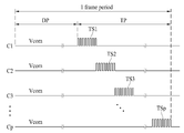
도 5는 1 프레임 기간의 디스플레이 구동기간과 터치 센싱기간 동안 공통라인들에 공급되는 공통전압과 터치신호들을 보여주는 파형도.
도 6은 도 3의 공통전압 보상부를 상세히 보여주는 회로도.
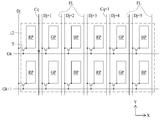
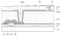
도 7은 액정표시패널의 화소들의 트랜지스터들, 화소전극들, 공통전극, 공통라인들, 및 피드백 라인들을 상세히 보여주는 일 예시도면.
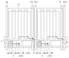
도 8은 도 7의 제j 데이터라인, 제j+1 데이터라인, 및 제k 게이트라인에 접속된 화소들을 상세히 보여주는 확대도.
도 9는 도 8의 I-I'의 단면도.
도 10은 도 8의 Ⅱ-Ⅱ'의 단면도.1 is a block diagram showing a liquid crystal display device according to an embodiment of the present invention;
FIG. 2 is an exemplary view showing details of data lines, gate lines, pixels, a gate driver, and a data driver of the liquid crystal display panel of FIG. 1;
3 is an exemplary view showing the pixel of FIG. 2 in detail;
FIG. 4 is a diagram illustrating common electrodes, common lines, feedback lines, a touch driver, and a common voltage compensating unit of the liquid crystal display panel of FIG. 1;
FIG. 5 is a waveform diagram showing common voltages and touch signals supplied to common lines during a display driving period and a touch sensing period of one frame period; FIG.
6 is a circuit diagram showing the common voltage compensation unit of FIG. 3 in detail;
7 is an exemplary view showing in detail the transistors, pixel electrodes, common electrodes, common lines, and feedback lines of pixels of a liquid crystal display panel.
8 is an enlarged view showing in detail the pixels connected to the jth data line, the (j + 1) th data line, and the kth gate line in Fig. 7;
9 is a sectional view taken along line I-I 'of Fig.
10 is a sectional view of II-II 'of FIG.
이하 첨부된 도면을 참조하여 본 발명에 따른 바람직한 실시예들을 상세히 설명한다. 명세서 전체에 걸쳐서 동일한 참조번호들은 실질적으로 동일한 구성요소들을 의미한다. 이하의 설명에서, 본 발명과 관련된 공지 기능 혹은 구성에 대한 구체적인 설명이 본 발명의 요지를 불필요하게 흐릴 수 있다고 판단되는 경우, 그 상세한 설명을 생략한다. 또한, 이하의 설명에서 사용되는 구성요소 명칭은 명세서 작성의 용이함을 고려하여 선택된 것일 수 있는 것으로서, 실제 제품의 부품 명칭과는 상이할 수 있다.
DETAILED DESCRIPTION OF THE PREFERRED EMBODIMENTS Reference will now be made in detail to the preferred embodiments of the present invention, examples of which are illustrated in the accompanying drawings. Like reference numerals throughout the specification denote substantially identical components. In the following description, a detailed description of known functions and configurations incorporated herein will be omitted when it may make the subject matter of the present invention rather unclear. In addition, the component names used in the following description may be selected in consideration of easiness of specification, and may be different from the parts names of actual products.
도 1은 본 발명의 실시예에 따른 액정표시장치를 보여주는 블록도이다. 도 2는 도 1의 액정표시패널의 데이터라인들, 게이트라인들, 화소들과 게이트 구동부, 및 데이터 구동부를 상세히 보여주는 일 예시도면이다. 도 3은 도 2의 화소를 상세히 보여주는 일 예시도면이다. 도 4는 도 1의 액정표시패널의 공통전극들, 공통라인들, 피드백 라인들과 터치 구동부, 및 공통전압 보상부를 보여주는 일 예시도면이다. 도 5는 1 프레임 기간의 디스플레이 구동기간과 터치 센싱기간 동안 공통전극들에 공급되는 공통전압과 터치신호들을 보여주는 파형도이다. 이하에서는 도 1 내지 도 5를 결부하여 본 발명의 실시예에 따른 액정표시장치에 대하여 개략적으로 설명한다.1 is a block diagram showing a liquid crystal display according to an embodiment of the present invention. FIG. 2 is an exemplary view showing details of data lines, gate lines, pixels, a gate driver, and a data driver of the liquid crystal display panel of FIG. 1; 3 is an exemplary view showing the pixel of FIG. 2 in detail. 4 is a diagram illustrating common electrodes, common lines, feedback lines, a touch driver, and a common voltage compensating unit of the liquid crystal display panel of FIG. 5 is a waveform diagram showing common voltages and touch signals supplied to common electrodes during a display driving period and a touch sensing period of one frame period. Hereinafter, a liquid crystal display according to an embodiment of the present invention will be schematically described with reference to FIGS. 1 to 5. FIG.
본 발명의 실시예에 따른 액정표시장치는 사용자가 손가락 또는 펜으로 터치를 하는 경우 사용자의 터치를 인식할 수 있는 터치 스크린 장치인 것을 중심으로 설명하였다. 특히, 본 발명의 실시예에 따른 액정표시장치는 자기 정전 용량(셀프 커패시턴스(self capacitance) 방식으로 사용자의 터치를 인식하는 것을 중심으로 설명하였다. 또한, 본 발명의 실시예에 따른 액정표시장치는 화상 표시와 터치 센싱을 모두 수행하기 위해, 도 5와 같이 디스플레이 구동기간(DP)과 터치 센싱기간(TP)을 시간적으로 분할하여 구동한다. 도 5에서는 1 프레임 기간(1 frame period)이 하나의 디스플레이 구동기간(DP)과 하나의 터치 센싱기간(TP)을 포함하는 것을 예시하였으나, 이에 한정되지 않음에 주의하여야 한다. 즉, 1 프레임 기간(1 frame period)은 복수의 디스플레이 구동기간(DP)과 복수의 터치 센싱기간(TP)을 포함할 수 있다.The liquid crystal display device according to the embodiment of the present invention has been mainly described as a touch screen device capable of recognizing the user's touch when the user touches the finger or the pen. In particular, the liquid crystal display device according to the embodiment of the present invention has been described mainly on the recognition of the user's touch by the self capacitance (self capacitance) method. 5, the display driving period DP and the touch sensing period TP are temporally divided and driven in order to perform both the image display and the touch sensing. In Fig. 5, one frame period (one frame period) The display driving period DP and the one touch sensing period TP are included but the present invention is not limited thereto. That is, one frame period is divided into a plurality of display driving periods DP, And a plurality of touch sensing periods (TP).
본 발명의 실시예에 따른 액정표시장치는 도 1과 같이 액정표시패널(10), 게이트 구동부(20), 데이터 구동부(30), 타이밍 제어부(40), 메인 프로세서(50), 터치 구동부(60), 및 공통전압 보상부(70)를 포함한다.1, a liquid crystal display device according to an embodiment of the present invention includes a liquid
액정표시패널(10)은 하부기판, 상부기판, 및 하부기판과 상부기판 사이에 개재된 액정층을 포함한다. 액정표시패널(10)의 하부기판에는 데이터라인들(D1~Dm, m은 2 이상의 양의 정수), 게이트라인들(G1~Gn, n은 2 이상의 양의 정수), 공통라인들(C1~Cp, p는 2 이상의 양의 정수), 및 피드백라인(FL)들이 형성된다. 데이터라인들(D1~Dm), 피드백라인(FL)들, 및 공통라인들(C1~Cp)은 게이트라인들(G1~Gn)과 교차될 수 있다.The liquid
데이터라인들(D1~Dm)과 게이트라인들(G1~Gn)의 교차부들에는 도 2와 같이 화소(P)들이 형성될 수 있다. 화소(P)들 각각은 데이터라인과 게이트라인에 접속될 수 있다. 화소(P)들 각각은 도 3과 같이 트랜지스터(T), 화소전극(11), 및 스토리지 커패시터(Cst)를 포함할 수 있다. 트랜지스터(T)는 제k(k는 1≤k≤n을 만족하는 양의 정수) 게이트라인(Gk)의 게이트신호에 의해 턴-온되어 제j(j는 1≤j≤m을 만족하는 양의 정수) 데이터라인(Dj)의 데이터전압을 화소전극(11)에 공급한다. 공통전극(12)은 공통라인들(C1~Cp) 중 어느 하나로부터 공통전압을 공급받는다. 이로 인해, 화소(P)들 각각은 화소전극(11)에 공급된 데이터전압과 공통전극(12)에 공급된 공통전압의 전위차에 의해 발생되는 전계에 의해 액정층(13)의 액정을 구동하여 백라이트 유닛으로부터 입사되는 빛의 투과량을 조정할 수 있다. 그 결과, 화소(P)들은 화상을 표시할 수 있다. 또한, 스토리지 커패시터(Cst)는 화소전극(11)과 공통전극(12) 사이에 마련되어 화소전극(11)과 공통전극(12) 간의 전압차를 일정하게 유지한다.Pixels P may be formed at the intersections of the data lines D1 to Dm and the gate lines G1 to Gn as shown in FIG. Each of the pixels P may be connected to the data line and the gate line. Each of the pixels P may include a transistor T, a
액정표시패널(10)에는 도 4와 같이 복수의 공통전극(12)들은 형성된다. 공통전극(12)들 각각은 도 7과 같이 복수의 화소들과 중첩되도록 형성될 수 있다. 예를 들어, 공통전극(12)들 각각은 s(s는 2 이상의 양의 정수) 개의 화소들과 중첩되도록 형성될 수 있다.A plurality of
공통전극(12)들 각각은 도 4와 같이 공통라인들(C1~Cp) 중 어느 하나에 접속될 수 있다. 공통라인들(C1~Cp) 각각은 공통전극(12)들 각각과 터치 구동부(60)를 연결한다. 이로 인해, 공통전극(12)들은 공통라인들(C1~Cp)을 통해 터치 구동부(60)로부터 도 5와 같이 디스플레이 구동기간(DP) 동안 공통전압을 공급받고, 터치 센싱기간(TP) 동안 터치신호들을 공급받을 수 있다. 공통라인들(C1~Cp)은 도 7과 같이 서로 인접한 두 개의 화소들 사이에 배치될 수 있다.Each of the
도 4와 같이 서로 인접한 두 개의 공통라인들 사이에는 피드백 라인(FL)이 배치될 수 있다. 도 4에서는 서로 인접한 두 개의 공통라인들 사이에 두 개의 피드백 라인(FL)들이 배치된 것을 예시하였으나, 이에 한정되지 않음에 주의하여야 한다. 또한, 피드백 라인(FL)들 각각은 도 7과 같이 서로 인접한 두 개의 화소들 사이에 배치될 수 있다. 피드백 라인(FL)들은 하나의 라인으로 묶여서 공통전압 보상부(70)에 접속된다.As shown in FIG. 4, a feedback line FL may be disposed between two adjacent common lines. In FIG. 4, two feedback lines (FL) are arranged between two adjacent common lines. However, it should be noted that the present invention is not limited thereto. Further, each of the feedback lines FL may be disposed between two adjacent pixels as shown in FIG. The feedback lines FL are grouped into one line and connected to the common
한편, 공통라인들(C1~Cp)로 인하여 공통전극(12)들에 공급되는 공통전압을 보상하기 위해 공통전압을 피드백받는 피드백 라인(FL)들을 설계하기 위한 공간이 부족할 수 있다. 따라서, 본 발명의 실시예는 피드백 라인(FL)들 각각을 공통전극(12)들 각각에 접속시키지 않고, 피드백 라인(FL)들 각각을 공통전극(12)들과 중첩되도록 형성한다. 피드백 라인(FL)들은 어떠한 전압도 인가되지 않는 플로팅 라인들(floating lines)일 수 있다. 플로팅 라인에는 어떠한 전압도 인가되지 않기 때문에, 플로팅 라인은 그에 인접한 라인 또는 전극의 전압 변화에 의해 쉽게 영향을 받는다. 결국, 피드백 라인(FL)들 각각은 플로팅 라인이기 때문에, 액정표시패널(10)에서 발생하는 불특정 노이즈(noise)에 의해 쉽게 영향을 받을 수 있다. 특히, 도 4와 같이 피드백 라인(FL)들 각각이 공통전극(12)들과 중첩되도록 형성되는 경우, 피드백 라인(FL)들 각각은 공통전극(12)들과 가장 인접하므로, 공통전극(12)들의 공통전압 변화량이 피드백 라인(FL)들 각각에 반영될 수 있다. 이 경우, 공통전압 보상부(70)는 액정표시패널(10)에서 발생한 불특정 노이즈(noise)에 의해 영향을 받은 공통전압 변화량을 피드백 라인(FL)들을 통해 입력받을 수 있으므로, 액정표시패널(10)의 노이즈를 반영하여 공통전압을 보상할 수 있다.On the other hand, there may be insufficient space for designing the feedback lines FL that receive the common voltage to compensate for the common voltage supplied to the
액정표시패널(10)의 상부기판에는 블랙매트릭스(black matrix)와 컬러필터(color filter) 등이 형성될 수 있다. 다만, 액정표시패널(10)이 COT(Color filter On TFT) 구조로 형성되는 경우, 블랙매트릭스와 컬러필터는 액정표시패널(10)의 하부기판에 형성될 수 있다.A black matrix, a color filter, and the like may be formed on the upper substrate of the liquid
액정표시패널(10)의 상부기판과 하부기판 각각에는 편광판이 부착되고 액정의 프리틸트각(pre-tilt angle)을 설정하기 위한 배향막이 형성된다. 액정표시패널(10)의 상부기판과 하부기판 사이에는 액정셀의 셀갭(cell gap)을 유지하기 위한 컬럼 스페이서가 형성된다.On the upper substrate and the lower substrate of the liquid
액정표시패널(10)의 하부기판의 배면 아래에는 백라이트 유닛이 배치될 수 있다. 백라이트 유닛은 에지형(edge type) 또는 직하형(Direct type) 백라이트 유닛으로 구현되어 액정표시패널(10)에 빛을 조사한다.A backlight unit may be disposed below the bottom surface of the lower substrate of the liquid
게이트 구동부(20)는 디스플레이 구동기간(DP) 동안 타이밍 제어부(40)로부터 입력되는 게이트 제어신호(GCS)에 따라 게이트신호들을 생성한다. 게이트 구동부(20)는 디스플레이 구동기간(DP) 동안 게이트신호들을 미리 정해진 순서대로 게이트라인들(G1~Gn)에 공급한다. 미리 정해진 순서는 순차적인 순서일 수 있다.The
데이터 구동부(30)는 디스플레이 구동기간(DP) 동안 타이밍 제어부(40)로부터 디지털 비디오 데이터(DATA)와 데이터 제어신호(DCS)를 입력받는다. 데이터 구동부(30)는 디스플레이 구동기간(DP) 동안 데이터 제어신호(DCS)에 따라 디지털 비디오 데이터(DATA)를 아날로그 데이터전압들로 변환한다. 데이터 구동부(30)는 디스플레이 구동기간(DP) 동안 데이터전압들을 데이터라인들(D1~Dm)에 공급한다.The
타이밍 제어부(40)는 메인 프로세서(50)로부터 디지털 비디오 데이터(DATA)와 타이밍 신호들을 입력받는다. 타이밍 신호들은 수직동기신호(vertical synchronization signal), 수평동기신호(horizontal synchronization signal), 데이터 인에이블 신호(data enable signal), 도트 클럭(dot clock) 등을 포함할 수 있다. 수직동기신호는 1 프레임 기간을 정의하는 신호이다. 수평동기신호는 액정표시패널(10)의 1 수평라인의 화소들에 데이터 전압들을 공급하는 1 수평기간을 정의하는 신호이다. 1 수평라인의 화소들은 동일한 게이트라인에 접속될 수 있다. 데이터 인에이블 신호는 유효한 디지털 비디오 데이터가 공급되는 기간을 정의하는 신호이다. 도트 클럭은 소정의 짧은 주기로 반복되는 신호이다.The
타이밍 제어부(40)는 액정표시장치를 표시모드와 센싱모드로 구분하여 동작시킨다. 타이밍 제어부(40)는 도 5와 같이 1 프레임 기간(1 frame period)의 디스플레이 구동기간(DP) 동안 액정표시장치를 표시모드로 동작시키고, 터치 센싱기간(TP) 동안 센싱모드로 동작시킬 수 있다. 타이밍 제어부(40)는 표시모드와 센싱모드를 구분하기 위해 모드신호(MODE)를 생성할 수 있다. 이 경우, 타이밍 제어부(40)는 디스플레이 구동기간(DP) 동안 제1 로직 레벨 전압의 모드신호(MODE)를 출력하고, 터치 센싱기간(TP) 동안 제2 로직 레벨 전압의 모드신호(MODE)를 출력할 수 있다.The
타이밍 제어부(40)는 타이밍 신호들에 기초하여 게이트 구동부(20)의 동작 타이밍을 제어하기 위한 게이트 제어신호(GCS)와 데이터 구동부(30)의 동작 타이밍을 제어하기 위한 데이터 제어신호(DCS)를 생성한다. 타이밍 제어부(40)는 터치 구동부(60)의 동작 타이밍을 제어하기 위한 터치 제어신호(TCS)를 생성한다. 타이밍 제어부(40)는 디스플레이 구동기간(DP) 동안 게이트 구동부(20)에 게이트 제어신호(GCS)를 출력하고, 데이터 구동부(30)에 디지털 비디오 데이터(DATA)와 데이터 타이밍 제어신호(DCS)를 출력할 수 있다. 타이밍 제어부(40)는 터치 구동부(60)에 터치 제어신호(TCS)와 모드신호(MODE)를 출력할 수 있다. 타이밍 제어부(40)는 공통전압 보상부(70)에 모드신호(MODE)를 출력할 수 있다.The
메인 프로세서(50)는 네비게이션 시스템, 셋톱박스, DVD 플레이어, 블루레이 플레이어, 개인용 컴퓨터(PC), 노트북, 홈 시어터 시스템, 방송 수신기, 스마트폰, 태블릿, 이동 단말기 중 어느 하나의 중앙처리장치(CPU), 호스트 프로세서(host processor), 어플리케이션 프로세서(application processor), 또는 그래픽 처리장치(GPU)로 구현될 수 있다. 메인 프로세서(50)은 디지털 비디오 데이터(DATA)를 액정표시패널(10)에 표시하기에 적합한 포맷으로 변환하여 타이밍 제어부(40)에 전송한다.The
또한, 메인 프로세서(50)은 터치 구동부(60)로부터 터치 좌표 데이터(CD)를 입력받을 수 있다. 메인 프로세서(50)는 터치 좌표 데이터(CD)에 따라 사용자에 의해 터치가 발생한 좌표와 연계된 응용 프로그램 또는 어플리케이션 프로그램을 실행할 수 있다. 메인 프로세서(50)는 실행 프로그램에 따른 디지털 비디오 데이터(DATA)와 타이밍 신호들을 타이밍 제어부(40)로 전송할 수 있다.In addition, the
터치 구동부(60)는 타이밍 제어부(40)로부터 터치 제어신호(TCS)와 모드신호(MODE)를 입력받는다. 터치 구동부(60)는 공통전압 보상부(70)로부터 공통전압(Vcom)을 입력받는다.The
터치 구동부(60)는 모드신호(MODE)에 따라 디스플레이 구동기간(DP)과 터치 센싱기간(TP)을 구분되어 동작할 수 있다. 터치 구동부(60)는 도 5와 같이 디스플레이 구동기간(DP) 동안 공통전압(Vcom)을 공통라인들(C1~Cp)을 통해 공통전극(12)들에 공급한다. 터치 구동부(60)는 터치 센싱기간(TP) 동안 터치 제어신호(TCS)에 따라 터치신호들(TS1~TSp)을 생성한다. 터치 구동부(60)는 도 5와 같이 터치 센싱기간(TP) 동안 터치신호들(TS1~TSp)을 공통라인들(C1~Cp)을 통해 공통전극(12)들에 공급한다.The
터치 구동부(60)는 터치신호들(TS1~TSp)을 미리 정해진 순서대로 공통라인들(C1~Cp)에 공급할 수 있다. 미리 정해진 순서는 순차적인 순서인 경우, 터치 구동부(60)는 제1 내지 제p 공통라인들(C1~Cp)에 제1 내지 제p 터치신호들(TS1~TSp)을 순차적으로 공급할 수 있다.The
터치신호들(TS1~TSp)은 복수 개의 펄스들을 포함할 수 있다. 도 5에서는 터치신호들(TS1~TSp)이 공통전압(Vcom)보다 높은 레벨의 전압을 갖는 것을 중심으로 설명하였으나, 이에 한정되지 않음에 주의하여야 한다.The touch signals TS1 to TSp may include a plurality of pulses. 5, the touch signals TS1 to TSp have a voltage higher than the common voltage Vcom. However, the present invention is not limited thereto.
터치 구동부(60)는 공통전극(12)들로부터 터치신호들(TS1~TSp)에 따른 터치 센싱신호들을 수신한다. 터치 구동부(60)는 터치 센싱신호들을 소정의 알고리즘을 이용하여 연산하여 터치 좌표(들)를 산출할 수 있다. 터치 구동부(60)는 터치 좌표(들)를 포함하는 터치 좌표 데이터(CD)를 메인 프로세서(50)로 공급한다. 이 경우, 메인 프로세서(50)는 터치 좌표 데이터(CD)에 따라 사용자에 의해 터치가 발생한 좌표와 연계된 응용 프로그램 또는 어플리케이션 프로그램을 실행하고, 실행 프로그램에 따른 디지털 비디오 데이터(DATA)와 타이밍 신호들을 타이밍 제어부(40)로 전송한다.The
공통전압 보상부(70)는 기준 공통전압라인(Vcom_REF)을 통해 전원 공급원으로부터 기준 공통전압을 입력받고, 타이밍 제어부(40)로부터 모드신호(MODE)를 입력받으며, 피드백 라인(FL)들로부터 공통전극(12)들의 공통전압 변화량을 입력받는다. 공통전압 보상부(70)는 모드신호(MODE)에 따라 디스플레이 구동기간(DP)과 터치 센싱기간(TP)으로 구분되어 동작한다. 터치 센싱기간(TP) 동안에는 공통전극(12)들에 터치신호들이 공급되기 때문에, 공통전압 보상부(70)는 디스플레이 구동기간(DP) 동안에만 피드백 라인(FL)들의 전압 변화량에 따라 공통전압을 보상한다. 구체적으로, 공통전압 보상부(70)는 기준 공통전압(Vcom_REF) 레벨에서 피드백 라인(FL)들에 반영된 공통전압 변화량을 반전 증폭함으로써, 액정표시패널(10)에서 발생한 불특정 노이즈(noise)에 의해 영향을 받은 공통전압 변화량을 보상한 공통전압을 출력할 수 있다. 공통전압 보상부(70)에 대한 자세한 설명은 도 6을 결부하여 후술한다.
The common
도 6은 도 3의 공통전압 보상부의 일 예를 상세히 보여주는 회로도이다. 본 발명의 실시예에 따른 공통전압 보상부(70)는 도 6에 도시된 바에 한정되지 않음에 주의하여야 한다. 즉, 공통전압 보상부(70)는 이미 공지된 다른 공통전압 보상회로를 이용하여 공통전압을 보상할 수 있다.FIG. 6 is a circuit diagram showing an example of the common voltage compensation unit of FIG. 3 in detail. Note that the common
도 6을 참조하면, 공통전압 보상부(70)는 제1 및 제2 입력단자들(IN1, IN2), 출력단자(OUT), 커패시터(C), 및 반전 증폭부(71)를 포함할 수 있다.6, the common
제1 입력단자(IN1)는 피드백 라인(FL)들이 묶여진 하나의 라인에 접속된다. 즉, 제1 입력단자(IN1)에는 피드백 라인(FL)들에 반영된 공통전극(12)들의 공통전압 변화량이 입력된다.The first input terminal IN1 is connected to one line to which the feedback lines FL are bundled. That is, a common voltage variation of the
제2 입력단자(IN2)는 기준 공통전압이 공급되는 기준 공통전압 라인(Vcom_REF)에 접속된다. 즉, 제2 입력단자(IN2)에는 기준 공통전압이 공급될 수 있다. 기준 공통전압은 전원 공급원에서 입력되는 직류전압이다.The second input terminal IN2 is connected to the reference common voltage line Vcom_REF to which the reference common voltage is supplied. That is, the reference common voltage may be supplied to the second input terminal IN2. The reference common voltage is the DC voltage input from the power supply source.
출력단자(OUT)는 터치 구동부(60)에 접속된다. 즉, 출력단자(OUT)로 출력되는 공통전압은 터치 구동부(60)에 입력된다.The output terminal (OUT) is connected to the touch driver (60). That is, the common voltage output to the output terminal OUT is input to the
커패시터(C)는 제1 입력단자(IN1)와 반전 증폭부(71) 사이에 마련된다. 커패시터(C)는 제1 입력단자(IN1)로 입력되는 공통전압 변화량을 반전 증폭부(71)의 OP-AMP(OP)의 반전 입력단자(-)에 공급한다.The capacitor C is provided between the first input terminal IN1 and the inverting amplifier 71. The capacitor C supplies the common voltage variation amount input to the first input terminal IN1 to the inverting input terminal (-) of the OP-AMP (OP) of the inverting amplifier 71. [
반전 증폭부(600)는 OP-AMP(OP), 제1 저항(R1) 및 제2 저항(R2)를 포함할 수 있다. OP-AMP(OP)는 제2 입력단자(IN2)에 접속되어 직류 전원전압인 기준 공통전압이 입력되는 비반전 입력단자(+), 제1 입력단자(VI1)에 접속되어 피드백전압이 입력되는 반전 입력단자(-), 및 출력 단자(o)를 포함한다. 제1 저항(R1)은 OP-AMP(OP)의 반전 입력단자(-)와 제1 전원 입력단자(VI1) 사이에 접속된다. 제2 저항(R2)는 OP-AMP(OP)의 반전 입력단자(-)와 출력 단자 사이에 접속된다. 반전 증폭부(600)는 제1 및 제2 저항들(R1, R2)의 저항비에 따라 OP-AMP(OP)의 비반전 입력단자(+)로 입력되는 기준 공통전압의 레벨에서 반전 입력단자(-)로 입력되는 공통전압 변화량을 반전 보상하여 출력단자(OUT)로 출력한다.The inverting
이상에서 살펴본 바와 같이, 본 발명의 실시예에 따른 공통전압 보상부(70)는 피드백 라인(FL)들에 반영된 공통전극(12)들의 공통전압 변화량을 입력받으므로, 공통전극(12)들이 영향을 받는 노이즈들을 모두 반영하여 공통전압(Vcom)을 보상할 수 있다.
As described above, since the common
도 7은 액정표시패널의 화소들의 트랜지스터들, 화소전극들, 공통전극, 공통라인들, 및 피드백 라인들을 상세히 보여주는 일 예시도면이다. 도 7에서는 설명의 편의를 위해 제j 내지 제j+5 데이터라인들(Dj~Dj+5), 제k 내지 제k+1 게이트라인들(Gk, Gk+1), 및 그들의 교차영역들에 마련된 트랜지스터(T)들과 화소전극들(RP, GP, BP)만을 예시하였다. 또한, 도 7에서는 화소전극이 적색 화소의 화소전극(RP), 녹색 화소의 화소전극(GP) 및 청색 화소의 화소전극(BP) 중 어느 하나인 것을 예시하였으나, 이에 한정되지 않음에 주의하여야 한다. 한편, 적색 화소의 화소전극(RP), 녹색 화소의 화소전극(GP) 및 청색 화소의 화소전극(BP)은 도 7과 같이 수평 방향(x축 방향)으로 차례로 반복하여 마련될 수 있다.7 is an exemplary view showing in detail the transistors, pixel electrodes, common electrode, common lines, and feedback lines of the pixels of the liquid crystal display panel. In FIG. 7, for convenience of explanation, the (j + 1) th to (j + 5) th data lines Dj to Dj + 5, the k to k + 1 gate lines Gk and Gk + Only the transistors T and the pixel electrodes RP, GP and BP are illustrated. In FIG. 7, the pixel electrode is one of the red pixel pixel electrode RP, the green pixel pixel electrode GP, and the blue pixel pixel electrode BP. However, the present invention is not limited thereto . On the other hand, the pixel electrode RP of the red pixel, the pixel electrode GP of the green pixel, and the pixel electrode BP of the blue pixel may be repeated in the horizontal direction (x axis direction) as shown in FIG.
도 7을 참조하면, 화소들 각각은 트랜지스터(T) 및 화소전극(RP, GP, BP)을 포함한다. 트랜지스터(T)는 게이트라인에 공급되는 게이트신호에 의해 턴-온되어 데이터라인의 데이터전압을 화소전극(RP, GP, BP)에 공급한다. 트랜지스터(T)의 게이트 전극은 게이트라인에 접속되고, 소스 전극은 데이터라인에 접속되며, 드레인 전극은 화소전극(RP, GP, BP)에 접속될 수 있다. 화소전극(RP, GP, BP)은 트랜지스터(T)를 통해 데이터전압을 공급받는다. 화소전극(RP, GP, BP)의 데이터전압과 공통전극(12)의 공통전압의 전위차에 의해 발생되는 전계에 의해 액정층(13)의 액정을 구동하여 백라이트 유닛으로부터 입사되는 빛의 투과량을 조정할 수 있다.Referring to Fig. 7, each of the pixels includes a transistor T and pixel electrodes RP, GP, BP. The transistor T is turned on by the gate signal supplied to the gate line to supply the data voltage of the data line to the pixel electrodes RP, GP, BP. The gate electrode of the transistor T may be connected to the gate line, the source electrode may be connected to the data line, and the drain electrode may be connected to the pixel electrodes RP, GP, BP. The pixel electrodes RP, GP, and BP are supplied with a data voltage through the transistor T. The liquid crystal of the
공통전극(12)은 s 개의 화소들과 중첩될 수 있다. 도 7에서는 공통전극(12)이 12 개의 화소들과 중첩된 것을 예시하였으나, 이에 한정되지 않음에 주의하여야 한다. 공통전극(12)은 도 7과 같이 제1 콘택홀(CNT1)을 통해 제q 공통라인(Cq)에 접속될 수 있다. 제1 콘택홀(CNT1)은 도 9와 같이 제2 보호막(PAS2)을 관통하여 제q 공통라인(Cq)을 노출시키는 홀이다. 공통전극(12)에 접속되지 않는 다른 공통라인(Cq+1)들은 공통전극(12)에 중첩될 수 있다.The
공통라인들(Cq, Cq+1) 각각은 서로 인접한 두 개의 화소전극들(RP, GP, BP) 사이에 배치될 수 있다. 예를 들어, 공통라인들(Cq, Cq+1) 각각은 도 7과 같이 적색 화소의 화소전극(RP)과 녹색 화소의 화소전극(GP) 사이에 배치될 수 있다. 하지만, 본 발명의 실시예는 이에 한정되지 않으며, 공통라인들(Cq, Cq+1)의 배치는 공통라인들(Cq, Cq+1)의 개수에 따라 달라질 수 있다. 공통라인들(Cq, Cq+1)의 개수는 공통전극(12)들의 개수에 의존한다. 즉, 공통라인들(Cq, Cq+1)의 개수가 많아서 적색 화소의 화소전극(RP)과 녹색 화소의 화소전극(GP) 사이마다 공통라인들(Cq, Cq+1)을 배치하더라도 공통라인들(Cq, Cq+1)을 모두 배치하지 못하는 경우, 공통라인들(Cq, Cq+1)은 녹색 화소의 화소전극(GP)과 청색 화소의 화소전극(BP) 사이들 또는 청색 화소의 화소전극(BP)과 적색 화소의 화소전극(RP) 사이들에 배치될 수 있다. 또한, 공통라인들(Cq, Cq+1)의 개수가 적은 경우 공통라인들(Cq, Cq+1)은 적색 화소의 화소전극(RP)과 녹색 화소의 화소전극(GP) 사이들 중 일부에만 배치할 수 있다.Each of the common lines Cq and Cq + 1 may be disposed between two adjacent pixel electrodes RP, GP, and BP. For example, each of the common lines Cq and Cq + 1 may be disposed between the pixel electrode RP of the red pixel and the pixel electrode GP of the green pixel, as shown in FIG. However, the embodiment of the present invention is not limited to this, and the arrangement of the common lines Cq and Cq + 1 may vary depending on the number of the common lines Cq and Cq + 1. The number of common lines (Cq, Cq + 1) depends on the number of common electrodes (12). That is, even if the common lines Cq and Cq + 1 are arranged between the pixel electrode RP of the red pixel and the pixel electrode GP of the green pixel because the number of the common lines Cq and Cq + 1 is large, The common lines Cq and Cq + 1 are not provided between the pixel electrode GP of the green pixel and the pixel electrode BP of the blue pixel or the pixel of the blue pixel And may be disposed between the electrode BP and the pixel electrode RP of the red pixel. When the number of the common lines Cq and Cq + 1 is small, the common lines Cq and Cq + 1 are formed only in a part of the space between the pixel electrode RP of the red pixel and the pixel electrode GP of the green pixel. Can be deployed.
피드백 라인(FL)은 서로 인접한 두 개의 공통라인들(Cq, Cq+1) 사이에 배치될 수 있다. 예를 들어, 두 개의 피드백 라인(FL)들이 도 7과 같이 제q 및 제q+1 공통라인들(Cq, Cq+1) 사이에 배치될 수 있다. 하지만, 본 발명의 실시예는 이에 한정되지 않으며, 피드백 라인(FL)들의 배치는 공통라인들(Cq, Cq+1)의 개수와 피드백 라인(FL)들의 개수에 따라 달라질 수 있다. 이는 공통라인들(Cq, Cq+1)의 개수가 많을수록 피드백 라인(FL)들을 설계하기 위한 공간이 부족하기 때문이다. 예를 들어, 공통라인들(Cq, Cq+1)의 개수가 피드백 라인(FL)들의 개수보다 더 많은 경우, 서로 인접한 두 개의 공통라인들(Cq, Cq+1) 사이에는 하나의 피드백 라인(FL)이 배치될 수 있다. 또한, 피드백 라인(FL)들의 개수가 공통라인들(Cq, Cq+1)의 개수보다 많은 경우 서로 인접한 두 개의 공통라인들(Cq, Cq+1) 사이에는 두 개 이상의 피드백 라인(FL)들이 배치될 수 있다.The feedback line FL may be disposed between two adjacent common lines Cq and Cq + 1. For example, two feedback lines FL may be disposed between the q-th and (q + 1) -th common lines Cq and Cq + 1 as shown in FIG. However, the embodiment of the present invention is not limited to this, and the arrangement of the feedback lines FL may vary depending on the number of the common lines Cq and Cq + 1 and the number of the feedback lines FL. This is because the larger the number of common lines Cq and Cq + 1 is, the less space is required to design the feedback lines FL. For example, when the number of common lines Cq, Cq + 1 is larger than the number of feedback lines FL, one feedback line (Cq, Cq + 1) FL may be disposed. Further, when the number of feedback lines FL is greater than the number of common lines Cq and Cq + 1, two or more feedback lines FL are formed between two adjacent common lines Cq and Cq + 1 .
피드백 라인(FL)들 각각은 서로 인접한 두 개의 화소전극들(RP, GP, BP) 사이에 배치될 수 있다. 예를 들어, 피드백 라인(FL)들은 도 7과 같이 녹색 화소의 화소전극(GP)과 청색 화소의 화소전극(BP) 사이들과 청색 화소의 화소전극(BP)과 적색 화소의 화소전극(RP) 사이들에 배치될 수 있다. 하지만, 본 발명의 실시예는 이에 한정되지 않으며, 피드백 라인(FL)들의 배치는 공통라인들(Cq, Cq+1)의 개수와 피드백 라인(FL)들의 개수에 따라 달라질 수 있다. 이는 공통라인들(Cq, Cq+1)의 개수가 많을수록 피드백 라인(FL)들을 설계하기 위한 공간이 부족하기 때문이다. 예를 들어, 공통라인들(Cq, Cq+1)의 개수가 피드백 라인(FL)들의 개수보다 더 많은 경우 피드백 라인(FL)들 각각은 녹색 화소의 화소전극(GP)과 청색 화소의 화소전극(BP) 사이들과 청색 화소의 화소전극(BP)과 적색 화소의 화소전극(RP) 사이들에 배치될 수 있다. 또한, 피드백 라인(FL)들의 개수가 공통라인들(Cq, Cq+1)의 개수보다 더 많은 경우 피드백 라인(FL)들 각각은 녹색 화소의 화소전극(GP)과 청색 화소의 화소전극(BP) 사이들 또는 청색 화소의 화소전극(BP)과 적색 화소의 화소전극(RP) 사이들에만 배치될 수 있다.Each of the feedback lines FL may be disposed between two adjacent pixel electrodes RP, GP, BP. For example, the feedback lines FL are formed between the pixel electrode GP of the green pixel and the pixel electrode BP of the blue pixel, the pixel electrode BP of the blue pixel and the pixel electrode RP of the red pixel, ). ≪ / RTI > However, the embodiment of the present invention is not limited to this, and the arrangement of the feedback lines FL may vary depending on the number of the common lines Cq and Cq + 1 and the number of the feedback lines FL. This is because the larger the number of common lines Cq and Cq + 1 is, the less space is required to design the feedback lines FL. For example, when the number of common lines Cq, Cq + 1 is greater than the number of feedback lines FL, each of the feedback lines FL is connected to the pixel electrode GP of the green pixel, (BP) and between the pixel electrode (BP) of the blue pixel and the pixel electrode (RP) of the red pixel. When the number of the feedback lines FL is larger than the number of the common lines Cq and Cq + 1, each of the feedback lines FL is connected to the pixel electrode GP of the green pixel and the pixel electrode BP of the blue pixel ) Or between the pixel electrode (BP) of the blue pixel and the pixel electrode (RP) of the red pixel.
피드백 라인(FL)들 각각은 공통전극(12)들과 중첩되도록 형성된다. 또한, 피드백 라인(FL)들은 어떠한 전압도 인가되지 않는 플로팅 라인들(floating lines)일 수 있다. 이로 인해, 피드백 라인(FL)들은 공통전극(12)들의 공통전압이 변화되는 경우 공통전압 변화량이 반영될 수 있다. 특히, 도 7과 같이 피드백 라인(FL)들 각각이 공통전극(12)들과 중첩되도록 형성되는 경우, 피드백 라인(FL)들은 공통전극(12)들에 가장 인접하므로, 공통전극(12)들의 공통전압 변화량이 피드백 라인(FL)들에 반영될 수 있다.Each of the feedback lines FL is formed to overlap with the
또한, 피드백 라인(FL)은 게이트라인들(Gk, Gk+1)과 교차되는 것이 바람직하다. 게이트라인들(Gk, Gk+1)에 게이트신호들이 미리 정해진 순서대로 공급되므로, 게이트신호들이 인가되는 게이트라인과 중첩되는 공통전극(12)이 게이트신호들 또는 화소전극에 공급되는 데이터전압에 의해 영향을 받을 가능성이 높다. 따라서, 피드백 라인(FL)들을 게이트라인들(Gk, Gk+1)과 교차되도록 설계하는 경우, 게이트신호들이 인가될때 공통전극(12)의 공통전압 변화량이 피드백 라인(FL)들에 반영될 수 있다. 그러므로, 공통전압 보상부(70)는 피드백 라인(FL)들에 반영된 공통전압 변화량을 보상한 공통전압(Vcom)을 출력할 수 있다.It is also preferable that the feedback line FL crosses the gate lines Gk and Gk + 1. Since the gate signals are supplied to the gate lines Gk and Gk + 1 in a predetermined order, the
이상에서 살펴본 바와 같이, 공통라인들(Cq, Cq+1)의 개수가 많을수록 피드백 라인(FL)들을 설계하기 위한 공간이 부족하기 때문에, 본 발명의 실시예는 피드백 라인(FL)들 각각을 공통전극(12)들 각각에 접속시키지 않고, 피드백 라인(FL)들 각각을 공통전극(12)들과 중첩되도록 형성한다. 이로 인해, 공통전극(12)과 피드백 라인(FL)들 간의 기생 용량에 의해 공통전극(12)의 공통전압 변화량이 피드백 라인(FL)들에 반영될 수 있다.
As described above, since the space for designing the feedback lines FL is insufficient as the number of the common lines Cq and Cq + 1 increases, Each of the feedback lines FL is formed so as to overlap with the
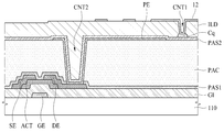
도 8은 도 7의 제j 데이터라인, 제j+1 데이터라인, 및 제k 게이트라인에 접속된 화소들을 상세히 보여주는 확대도이다. 도 9는 도 8의 I-I'의 단면도이다. 도 10은 도 8의 Ⅱ-Ⅱ'의 단면도이다. 도 8 내지 도 10에서는 본 발명의 실시예에 따른 액정표시패널(10)이 IPS(In-Plane Switching) 모드 또는 FFS(Fringe Field Switching) 모드와 같은 수평전계 구동방식으로 구현된 것을 중심으로 설명하였으나, 이에 한정되지 않음에 주의하여야 한다. 이하에서는, 도 8 내지 도 10을 결부하여 본 발명의 실시예에 따른 제q 공통라인(Cq)과 공통전극(12)의 접속, 피드백 라인(FL)에 대하여 상세히 살펴본다.8 is an enlarged view showing pixels connected to the jth data line, the (j + 1) th data line, and the kth gate line in FIG. 7 in detail. 9 is a sectional view taken along the line I-I 'in Fig. 10 is a sectional view of II-II 'of FIG. 8 to 10, the liquid
도 8 내지 도 10을 참조하면, 하부기판(110)상에 트랜지스터(T)의 게이트 전극(GE)을 포함하는 게이트 금속층이 형성된다. 게이트 금속층은 몰리브덴(Mo)으로 형성될 수 있다. 게이트 금속층은 하부기판(110)의 버퍼층(미도시) 상에 형성될 수도 있다. 게이트 금속층은 제1 금속층으로 정의될 수 있다.8 to 10, a gate metal layer including a gate electrode GE of a transistor T is formed on a
제1 금속층 상에는 게이트 절연막(GI)이 형성된다. 게이트 절연막(GI)은 실리콘나이트라이드(SiNx)로 형성될 수 있다.A gate insulating film GI is formed on the first metal layer. The gate insulating film GI may be formed of silicon nitride (SiNx).
게이트 절연막(GI) 상에는 트랜지스터(T)의 반도체층(ACT)이 형성된다. 반도체층(ACT)은 게이트 전극(GE)에 중첩되게 형성된다. 반도체층(ACT)은 a-Si, 산화물 반도체, 폴리 실리콘 중 어느 하나로 형성될 수도 있다. 제1 금속층과 반도체층(ACT)은 게이트 절연막(GI)에 의해 절연된다.A semiconductor layer (ACT) of the transistor (T) is formed on the gate insulating film (GI). The semiconductor layer ACT is formed to overlap the gate electrode GE. The semiconductor layer (ACT) may be formed of any one of a-Si, an oxide semiconductor, and polysilicon. The first metal layer and the semiconductor layer (ACT) are insulated by a gate insulating film (GI).
반도체층(ACT) 상에는 제j 및 제j+1 데이터라인들(Dj, Dj+1), 트랜지스터(T)의 소스 전극(SE)과 드레인 전극(DE)을 포함하는 소스/드레인 금속층이 형성된다. 소스/드레인 금속층은 티타늄(Ti)/알루미늄(Al)/티타늄(Ti)의 3층 구조로 형성될 수 있다. 소스/드레인 금속층은 제2 금속층으로 정의될 수 있다.A source / drain metal layer including the source electrode SE and the drain electrode DE of the jth and j + 1th data lines Dj and Dj + 1 and the transistor T is formed on the semiconductor layer ACT . The source / drain metal layer may be formed in a three-layer structure of titanium (Ti) / aluminum (Al) / titanium (Ti). The source / drain metal layer may be defined as a second metal layer.
반도체층(ACT)과 제2 금속층 상에는 제1 보호막(PAS1)과 평탄화막(PAC)이 차례로 형성될 수 있다. 제1 보호막(PAS1)은 실리콘나이트라이드(SiNx)로 형성될 수 있다. 평탄화막(PAC)은 포토 아크릴(photo acryl)로 형성할 수 있다.The first protective film PAS1 and the planarization film PAC may be sequentially formed on the semiconductor layer ACT and the second metal layer. The first protective film PAS1 may be formed of silicon nitride (SiNx). The planarizing film (PAC) may be formed of photo acryl.
평탄화막(PAC) 상에는 화소전극(PE)을 포함하는 제1 투명전극층이 형성된다. 제1 투명전극층은 ITO, IZO 중 어느 하나로 형성될 수 있다. 제1 투명전극층과 제2 금속층은 제1 보호막(PAS1)과 평탄화막(PAC)에 의해 절연된다. 다만, 화소전극(PE)과 트랜지스터(T)의 드레인 전극(DE)은 제2 콘택홀(CNT2)을 통해 접속된다. 제2 콘택홀(CNT2)은 제1 보호막(PAS1)과 평탄화막(PAC)을 관통하여 트랜지스터(T)의 드레인 전극(DE)을 노출시킨다.A first transparent electrode layer including a pixel electrode PE is formed on the planarization layer PAC. The first transparent electrode layer may be formed of any one of ITO and IZO. The first transparent electrode layer and the second metal layer are insulated by the first passivation film (PAS1) and the planarization film (PAC). However, the pixel electrode PE and the drain electrode DE of the transistor T are connected through the second contact hole CNT2. The second contact hole CNT2 exposes the drain electrode DE of the transistor T through the first passivation film PAS1 and the planarization film PAC.
제1 투명전극층 상에는 제2 보호막(PAS2)이 형성된다. 제2 보호막(PAS2)은 실리콘나이트라이드(SiNx)로 형성될 수 있다.A second protective film PAS2 is formed on the first transparent electrode layer. The second protective film PAS2 may be formed of silicon nitride (SiNx).
제2 보호막(PAS2) 상에는 제q 공통라인(Cq)과 피드백 라인(FL)을 포함하는 제3 금속층이 형성될 수 있다. 제1 투명전극층과 제3 금속층은 제2 보호막(PAS2)에 의해 절연된다.A third metal layer including the qth common line Cq and the feedback line FL may be formed on the second protective film PAS2. The first transparent electrode layer and the third metal layer are insulated by the second protective film PAS2.
제3 금속층 상에는 층간 절연막(ILD)이 형성될 수 있다. 층간 절연막(ILD)은 실리콘나이트라이드(SiNx)로 형성될 수 있다.An interlayer insulating film (ILD) may be formed on the third metal layer. The interlayer insulating film (ILD) may be formed of silicon nitride (SiNx).
층간 절연막(ILD) 상에는 공통전극(12)을 포함하는 제2 투명전극층이 형성된다. 제2 투명전극층은 ITO, IZO 중 어느 하나로 형성될 수 있다. 제1 투명전극층과 제3 금속층은 층간 절연막(ILD)에 의해 절연된다. 공통전극(12)과 제q 공통라인(Cq)은 서로 다른 금속층에 마련되므로, 공통전극(12)과 제q 공통라인(Cq)은 제1 콘택홀(CNT1)을 통해 접속된다. 제1 콘택홀(CNT1)은 층간 절연막(ILD)을 관통하여 제q 공통라인(Cq)을 노출시킨다. 공통전극(12)은 화소전극(PE)과 중첩되게 형성되며, 화소전극(PE)과 수평전계를 형성하기 위해 화소전극(PE)을 노출시키는 소정의 홀들을 포함할 수 있다.A second transparent electrode layer including the
한편, 피드백 라인(FL)은 도 10과 같이 다른 전극 또는 라인에 접속되지 않으므로, 플로팅(floating)된다. 또한, 피드백 라인(FL)은 도 10과 같이 공통전극(12)과 중첩되므로, 피드백 라인(FL)과 공통전극(12) 사이에는 기생 용량(Cp)이 존재할 수 있다. 이로 인해, 공통전극(12)의 공통전압이 액정표시패널(10) 내에서 발생하는 블특정 노이즈(noise)에 의해 영향을 받아 변화되는 경우, 공통전극(12)의 공통전압은 기생 용량(Cp)에 의해 피드백 라인(FL)에 반영될 수 있다. 특히, 본 발명의 실시예는 피드백 라인(FL)들을 공통전극(12)들 모두에 중첩되게 형성하므로, 공통전극(12)들이 영향을 받는 노이즈들을 모두 반영하여 공통전압을 보상할 수 있다.On the other hand, the feedback line FL is not connected to another electrode or line as shown in FIG. 10, and therefore, it is floated. The parasitic capacitance Cp may exist between the feedback line FL and the
이상 설명한 내용을 통해 당업자라면 본 발명의 기술사상을 일탈하지 아니하는 범위에서 다양한 변경 및 수정이 가능함을 알 수 있을 것이다. 따라서, 본 발명의 기술적 범위는 명세서의 상세한 설명에 기재된 내용으로 한정되는 것이 아니라 특허 청구의 범위에 의해 정하여져야만 할 것이다.
It will be apparent to those skilled in the art that various modifications and variations can be made in the present invention without departing from the spirit or scope of the invention. Therefore, the technical scope of the present invention should not be limited to the contents described in the detailed description of the specification, but should be defined by the claims.
10: 표시패널
11, PE: 화소전극
12: 공통전극
13: 액정층
20: 게이트 구동부
30: 데이터 구동부
40: 타이밍 제어부
50: 메인 프로세서
60: 터치 구동부
70: 공통전압 보상부
FL: 피드백 라인
C1~Cp: 공통라인10:
12: common electrode 13: liquid crystal layer
20: Gate driver 30: Data driver
40: timing controller 50: main processor
60: touch driver 70: common voltage compensator
FL: feedback line C1 to Cp: common line
Claims (10)
상기 피드백 라인들의 전압 변화량에 따라 상기 공통전압을 보상하는 공통전압 보상부를 구비하고,
상기 공통전극은 상기 화소들 중 일부에 중첩되며,
상기 피드백 라인들은 상기 공통전극에 중첩되는 것을 특징으로 하는 액정표시장치.And a plurality of common electrodes to which a common voltage is supplied, the plurality of common electrodes being supplied with data voltages, data lines, feedback lines, gate lines crossing the data lines, pixels provided at intersections of the data lines and the gate lines, A liquid crystal display panel; And
And a common voltage compensation unit for compensating for the common voltage according to a voltage change amount of the feedback lines,
The common electrode is superimposed on a part of the pixels,
And the feedback lines overlap the common electrode.
상기 피드백 라인은 서로 인접한 어느 두 개의 화소들 사이에 마련되는 것을 특징으로 하는 액정표시장치.The method according to claim 1,
Wherein the feedback line is provided between two adjacent pixels.
상기 피드백 라인들은 상기 게이트라인들과 교차하는 것을 특징으로 액정표시장치.The method according to claim 1,
And the feedback lines cross the gate lines.
상기 피드백 라인들은 어떠한 전압도 인가되지 않은 플로팅 라인들인 것을 특징으로 하는 액정표시장치.The method according to claim 1,
Wherein the feedback lines are floating lines to which no voltage is applied.
상기 액정표시패널은 상기 공통전극들에 접속되는 공통라인들을 더 포함하고,
상기 피드백 라인은 상기 공통라인들 사이에 배치되는 것을 특징으로 하는 액정표시장치.The method according to claim 1,
Wherein the liquid crystal display panel further includes common lines connected to the common electrodes,
And the feedback lines are disposed between the common lines.
상기 공통라인은 서로 인접한 또 다른 두 개의 화소들 사이에 마련되는 것을 특징으로 하는 액정표시장치.6. The method of claim 5,
Wherein the common line is provided between two adjacent pixels adjacent to each other.
상기 공통전극은 상기 공통라인을 노출시키는 콘택홀을 통해 상기 공통라인에 접속되는 것을 특징으로 하는 액정표시장치.6. The method of claim 5,
And the common electrode is connected to the common line through a contact hole exposing the common line.
상기 데이터라인들에 데이터전압들을 공급하는 데이터 구동부;
상기 게이트라인들에 미리 정해진 순서대로 게이트신호들을 공급하는 게이트 구동부; 및
표시모드에서 상기 공통라인들에 공통전압을 공급하고, 터치모드에서 상기 공통라인들에 터치신호들을 공급하는 터치 구동부를 더 구비하는 액정표시장치.6. The method of claim 5,
A data driver for supplying data voltages to the data lines;
A gate driver for supplying gate signals to the gate lines in a predetermined order; And
And a touch driver for supplying a common voltage to the common lines in a display mode and supplying touch signals to the common lines in a touch mode.
상기 게이트라인들은 제1 금속층에 마련되고, 상기 데이터라인들은 상기 제1 금속층을 덮는 게이트 절연막 상의 제2 금속층에 마련되며, 상기 화소들의 화소전극들은 상기 제2 금속층을 덮는 평탄화막 상의 제1 투명전극층에 마련되고, 상기 공통라인들과 상기 피드백 라인들은 상기 제1 투명전극층을 덮는 제2 보호막 상의 제3 금속층에 마련되며, 상기 공통전극은 상기 제3 금속층을 덮는 층간 절연막 상의 제2 투명전극층에 마련되는 것을 특징으로 하는 액정표시장치.6. The method of claim 5,
Wherein the gate lines are provided in a first metal layer, the data lines are provided in a second metal layer on a gate insulating film covering the first metal layer, pixel electrodes of the pixels are formed in a first transparent electrode layer on a planarization layer covering the second metal layer, Wherein the common lines and the feedback lines are provided in a third metal layer on a second protective film covering the first transparent electrode layer and the common electrode is provided in a second transparent electrode layer on an interlayer insulating film covering the third metal layer And the liquid crystal display device.
상기 공통전압 보상부는,
상기 피드백 라인들에 접속된 제1 입력단자;
기준 공통전압이 공급되는 제2 입력단자;
상기 제1 입력단자로 입력되는 상기 피드백 라인들의 전압 변화량을 제1 노드로 부스팅하는 커패시터;
상기 제2 입력단자로 입력되는 상기 기준 공통전압 레벨에서 상기 제1 노드에 반영된 상기 피드백 라인들의 전압 변화량을 반전 증폭하여 보상 공통전압을 출력하는 반전 증폭부; 및
상기 공통라인들에 접속되어 보상 공통전압을 상기 공통라인들로 출력하는 출력단자를 포함하는 것을 특징으로 하는 액정표시장치.The method according to claim 1,
Wherein the common-
A first input terminal connected to the feedback lines;
A second input terminal to which a reference common voltage is supplied;
A capacitor for boosting a voltage variation of the feedback lines input to the first input terminal to a first node;
An inverting amplifier for inverting and amplifying a voltage variation of the feedback lines reflected at the first node at the reference common voltage level input to the second input terminal to output a compensating common voltage; And
And an output terminal connected to the common lines and outputting a compensated common voltage to the common lines.
Priority Applications (5)
| Application Number | Priority Date | Filing Date | Title |
|---|---|---|---|
| KR1020140186117A KR102335818B1 (en) | 2014-12-22 | 2014-12-22 | Liquid crystal display device |
| US14/923,051 US10372257B2 (en) | 2014-12-22 | 2015-10-26 | Liquid crystal display device having a common voltage compensator |
| JP2015210624A JP6246774B2 (en) | 2014-12-22 | 2015-10-27 | Liquid crystal display |
| TW104135357A TWI581244B (en) | 2014-12-22 | 2015-10-28 | Liquid crystal display device |
| CN201510762965.9A CN105717717B (en) | 2014-12-22 | 2015-11-10 | Liquid crystal display device |
Applications Claiming Priority (1)
| Application Number | Priority Date | Filing Date | Title |
|---|---|---|---|
| KR1020140186117A KR102335818B1 (en) | 2014-12-22 | 2014-12-22 | Liquid crystal display device |
Publications (2)
| Publication Number | Publication Date |
|---|---|
| KR20160077302A true KR20160077302A (en) | 2016-07-04 |
| KR102335818B1 KR102335818B1 (en) | 2021-12-06 |
Family
ID=56130135
Family Applications (1)
| Application Number | Title | Priority Date | Filing Date |
|---|---|---|---|
| KR1020140186117A Active KR102335818B1 (en) | 2014-12-22 | 2014-12-22 | Liquid crystal display device |
Country Status (5)
| Country | Link |
|---|---|
| US (1) | US10372257B2 (en) |
| JP (1) | JP6246774B2 (en) |
| KR (1) | KR102335818B1 (en) |
| CN (1) | CN105717717B (en) |
| TW (1) | TWI581244B (en) |
Cited By (2)
| Publication number | Priority date | Publication date | Assignee | Title |
|---|---|---|---|---|
| KR20180059237A (en) * | 2016-11-25 | 2018-06-04 | 엘지디스플레이 주식회사 | In-cell touch display device |
| KR20210083610A (en) * | 2019-12-27 | 2021-07-07 | 엘지디스플레이 주식회사 | Image display device comprising panel stabilizing circuit and method for panel stabilizing |
Families Citing this family (24)
| Publication number | Priority date | Publication date | Assignee | Title |
|---|---|---|---|---|
| CN104820514B (en) * | 2015-04-01 | 2017-05-10 | 上海中航光电子有限公司 | Touch display panel and driving method thereof |
| CN104866153B (en) * | 2015-05-29 | 2018-01-16 | 武汉华星光电技术有限公司 | Self-capacitance in-cell touch panel and preparation method thereof, liquid crystal display |
| CN105717690A (en) * | 2016-04-27 | 2016-06-29 | 武汉华星光电技术有限公司 | Embedded touch screen, preparation method thereof and liquid crystal display |
| KR102618596B1 (en) * | 2016-09-30 | 2023-12-28 | 엘지디스플레이 주식회사 | Display Device Having Touch Sensor |
| TWI585499B (en) * | 2016-10-26 | 2017-06-01 | 友達光電股份有限公司 | Display panel |
| KR102617273B1 (en) | 2016-10-31 | 2023-12-21 | 엘지디스플레이 주식회사 | In-cell touch display device |
| CN106873204B (en) * | 2017-02-21 | 2020-04-21 | 合肥鑫晟光电科技有限公司 | Display device, manufacturing method and driving method thereof, and counter substrate |
| CN106855763B (en) * | 2017-03-10 | 2020-02-07 | 武汉华星光电技术有限公司 | Array substrate and self-contained embedded touch display panel |
| KR102364630B1 (en) * | 2017-09-11 | 2022-02-17 | 엘지디스플레이 주식회사 | Touch Display Device |
| TWI653615B (en) * | 2018-04-19 | 2019-03-11 | 瑞鼎科技股份有限公司 | Drive circuit and its operation method |
| CN108986756B (en) * | 2018-07-17 | 2020-04-28 | 深圳市华星光电半导体显示技术有限公司 | Common voltage feedback compensation circuit and method and liquid crystal display device |
| CN108957814B (en) * | 2018-08-29 | 2021-08-13 | 南京京东方显示技术有限公司 | Liquid crystal display device and circuit compensation method |
| US10788718B2 (en) * | 2018-11-28 | 2020-09-29 | Panasonic Liquid Crystal Display Co., Ltd. | Liquid crystal display device |
| CN109473078B (en) * | 2019-01-02 | 2020-08-28 | 合肥京东方显示技术有限公司 | Common voltage regulating circuit and method, display driving circuit and display device |
| US11205363B2 (en) * | 2019-10-18 | 2021-12-21 | Apple Inc. | Electronic display cross-talk compensation systems and methods |
| CN111243538B (en) * | 2020-02-14 | 2022-08-09 | 京东方科技集团股份有限公司 | Common voltage compensation method and device for display panel, display panel and device |
| CN111443826B (en) * | 2020-03-27 | 2022-05-31 | 深圳市华星光电半导体显示技术有限公司 | Display panel compensation method and device |
| KR102857714B1 (en) * | 2020-12-28 | 2025-09-09 | 엘지디스플레이 주식회사 | Touch display device, touch driving circuit and display panel |
| CN117270267A (en) | 2022-06-15 | 2023-12-22 | 瀚宇彩晶股份有限公司 | Display panel and manufacturing method thereof |
| KR20240120366A (en) | 2023-01-31 | 2024-08-07 | 엘지디스플레이 주식회사 | Display device |
| WO2024178612A1 (en) * | 2023-02-28 | 2024-09-06 | 京东方科技集团股份有限公司 | Array substrate, display apparatus and heating drive method for display apparatus |
| CN116168660B (en) * | 2023-04-26 | 2023-08-08 | 惠科股份有限公司 | Driving circuit, display device and driving method of display panel |
| KR20250019748A (en) * | 2023-08-01 | 2025-02-11 | 삼성디스플레이 주식회사 | Display device, data driver, and method of driving display device |
| CN120808723A (en) * | 2025-07-31 | 2025-10-17 | 惠科股份有限公司 | Display panel and display device |
Citations (4)
| Publication number | Priority date | Publication date | Assignee | Title |
|---|---|---|---|---|
| JPH06186530A (en) * | 1992-12-16 | 1994-07-08 | Matsushita Electric Ind Co Ltd | Active matrix liquid crystal panel and its driving method |
| US5434599A (en) * | 1992-05-14 | 1995-07-18 | Kabushiki Kaisha Toshiba | Liquid crystal display device |
| KR20010030279A (en) * | 1999-09-06 | 2001-04-16 | 마찌다 가쯔히꼬 | Active-matrix-type liquid crystal display device, data signal line driving circuit, and liquid crystal display device driving method |
| JP2013122752A (en) * | 2011-12-09 | 2013-06-20 | Lg Display Co Ltd | Touch screen integrated display device |
Family Cites Families (21)
| Publication number | Priority date | Publication date | Assignee | Title |
|---|---|---|---|---|
| JP3288142B2 (en) * | 1992-10-20 | 2002-06-04 | 富士通株式会社 | Liquid crystal display device and driving method thereof |
| JP2004191581A (en) * | 2002-12-10 | 2004-07-08 | Sharp Corp | Liquid crystal display device and driving method thereof |
| KR100847823B1 (en) | 2003-12-04 | 2008-07-23 | 엘지디스플레이 주식회사 | LCD Display |
| KR101263512B1 (en) | 2006-06-12 | 2013-05-13 | 엘지디스플레이 주식회사 | Liquid Crystal Display Device And Driving Method Thereof |
| TWI451389B (en) | 2007-07-13 | 2014-09-01 | Innolux Corp | Liquid crystal display and method of driving a common voltage |
| JP2009128825A (en) * | 2007-11-27 | 2009-06-11 | Funai Electric Co Ltd | Liquid crystal display device |
| KR101513271B1 (en) * | 2008-10-30 | 2015-04-17 | 삼성디스플레이 주식회사 | Display device |
| TW201120858A (en) | 2009-12-15 | 2011-06-16 | Innolux Display Corp | Liquid crystal display device |
| KR101398238B1 (en) * | 2010-10-01 | 2014-05-22 | 엘지디스플레이 주식회사 | Display device having touch screen panel |
| CN102650916B (en) * | 2011-02-25 | 2014-11-26 | 乐金显示有限公司 | Touch sensor integrated display device |
| KR101503103B1 (en) * | 2011-03-25 | 2015-03-17 | 엘지디스플레이 주식회사 | Touch sensor integrated type display and driving method therefrom |
| KR101971147B1 (en) * | 2012-04-09 | 2019-04-23 | 삼성디스플레이 주식회사 | Display device including touch sensor |
| CN103295540B (en) * | 2012-06-07 | 2015-06-10 | 上海天马微电子有限公司 | Driving method and driving device of active matrix display panel and display |
| KR101448498B1 (en) | 2012-06-13 | 2014-10-08 | 엘지디스플레이 주식회사 | Display device with integrated touch screen |
| KR101356968B1 (en) * | 2012-06-14 | 2014-02-03 | 엘지디스플레이 주식회사 | Display device with integrated touch screen |
| KR101977592B1 (en) * | 2012-07-24 | 2019-05-13 | 엘지디스플레이 주식회사 | Liquid crystal display device inculding common voltage compensating circiut |
| CN102842280B (en) | 2012-08-31 | 2016-03-30 | 京东方科技集团股份有限公司 | A kind of common electric voltage compensating circuit, method and liquid crystal indicator |
| CN104035615B (en) | 2014-05-20 | 2016-03-02 | 京东方科技集团股份有限公司 | A kind of touch display panel and display device |
| CN104022128B (en) | 2014-05-30 | 2017-02-15 | 京东方科技集团股份有限公司 | Array substrate, manufacturing method thereof and displaying device |
| KR102305323B1 (en) * | 2014-09-10 | 2021-09-28 | 엘지디스플레이 주식회사 | Touch sensing device |
| CN104281352B (en) * | 2014-10-13 | 2017-06-06 | 京东方科技集团股份有限公司 | A kind of In-cell touch panel and display device |
-
2014
- 2014-12-22 KR KR1020140186117A patent/KR102335818B1/en active Active
-
2015
- 2015-10-26 US US14/923,051 patent/US10372257B2/en active Active
- 2015-10-27 JP JP2015210624A patent/JP6246774B2/en active Active
- 2015-10-28 TW TW104135357A patent/TWI581244B/en active
- 2015-11-10 CN CN201510762965.9A patent/CN105717717B/en active Active
Patent Citations (5)
| Publication number | Priority date | Publication date | Assignee | Title |
|---|---|---|---|---|
| US5434599A (en) * | 1992-05-14 | 1995-07-18 | Kabushiki Kaisha Toshiba | Liquid crystal display device |
| JPH06186530A (en) * | 1992-12-16 | 1994-07-08 | Matsushita Electric Ind Co Ltd | Active matrix liquid crystal panel and its driving method |
| KR20010030279A (en) * | 1999-09-06 | 2001-04-16 | 마찌다 가쯔히꼬 | Active-matrix-type liquid crystal display device, data signal line driving circuit, and liquid crystal display device driving method |
| JP2001147420A (en) * | 1999-09-06 | 2001-05-29 | Sharp Corp | Active matrix type liquid crystal display device, data signal line driving circuit, and driving method of liquid crystal display device |
| JP2013122752A (en) * | 2011-12-09 | 2013-06-20 | Lg Display Co Ltd | Touch screen integrated display device |
Cited By (2)
| Publication number | Priority date | Publication date | Assignee | Title |
|---|---|---|---|---|
| KR20180059237A (en) * | 2016-11-25 | 2018-06-04 | 엘지디스플레이 주식회사 | In-cell touch display device |
| KR20210083610A (en) * | 2019-12-27 | 2021-07-07 | 엘지디스플레이 주식회사 | Image display device comprising panel stabilizing circuit and method for panel stabilizing |
Also Published As
| Publication number | Publication date |
|---|---|
| KR102335818B1 (en) | 2021-12-06 |
| US20160180781A1 (en) | 2016-06-23 |
| CN105717717A (en) | 2016-06-29 |
| JP2016118767A (en) | 2016-06-30 |
| US10372257B2 (en) | 2019-08-06 |
| JP6246774B2 (en) | 2017-12-13 |
| CN105717717B (en) | 2018-09-21 |
| TWI581244B (en) | 2017-05-01 |
| TW201624458A (en) | 2016-07-01 |
Similar Documents
| Publication | Publication Date | Title |
|---|---|---|
| KR102335818B1 (en) | Liquid crystal display device | |
| KR102717057B1 (en) | In-cell touch display device | |
| US10338711B2 (en) | Display device, method of driving the same, and driving circuit thereof | |
| CN104252266B (en) | Drive the apparatus and method of touch-screen | |
| CN106557195B (en) | Show equipment and its driving method | |
| US9891747B2 (en) | Multi-touch sensitive display device and method for assigning touch identification therein | |
| US9601067B2 (en) | In-cell multi-touch display panel system | |
| KR102045809B1 (en) | Touch sensor integrated type display device | |
| KR20220038653A (en) | Display device | |
| KR102045808B1 (en) | Touch sensor integrated type display device | |
| US9690420B2 (en) | Display device having touch sensor | |
| KR102020935B1 (en) | Display device having touch sensors and control method of gate driving circuit thereof | |
| US20150109227A1 (en) | Touch sensing system and driving method thereof | |
| KR20160083405A (en) | Touch screen device and method for driving the same | |
| KR102504495B1 (en) | Touch sensor integrated type display device | |
| KR20130033562A (en) | Apparatus and method for driving touch screen | |
| KR20130004658A (en) | Liquid crystal display device with interred touch screen | |
| KR101323044B1 (en) | Touch sensing apparatus and driving method thereof | |
| KR101808348B1 (en) | Data processing method and apparatus for touch screen | |
| KR20160042351A (en) | Touch sensing system | |
| KR101904471B1 (en) | Touch sensing apparatus | |
| KR102272952B1 (en) | Touch sensing device and driving method thereof | |
| KR102440138B1 (en) | Touch screen integrated display device and driving method thereof | |
| KR102285909B1 (en) | Touch sensor intergrated type display device | |
| KR20130068551A (en) | Apparatus and method for driving touch screen |
Legal Events
| Date | Code | Title | Description |
|---|---|---|---|
| PA0109 | Patent application |
St.27 status event code: A-0-1-A10-A12-nap-PA0109 |
|
| PG1501 | Laying open of application |
St.27 status event code: A-1-1-Q10-Q12-nap-PG1501 |
|
| A201 | Request for examination | ||
| PA0201 | Request for examination |
St.27 status event code: A-1-2-D10-D11-exm-PA0201 |
|
| E902 | Notification of reason for refusal | ||
| PE0902 | Notice of grounds for rejection |
St.27 status event code: A-1-2-D10-D21-exm-PE0902 |
|
| P11-X000 | Amendment of application requested |
St.27 status event code: A-2-2-P10-P11-nap-X000 |
|
| P13-X000 | Application amended |
St.27 status event code: A-2-2-P10-P13-nap-X000 |
|
| E902 | Notification of reason for refusal | ||
| PE0902 | Notice of grounds for rejection |
St.27 status event code: A-1-2-D10-D21-exm-PE0902 |
|
| E13-X000 | Pre-grant limitation requested |
St.27 status event code: A-2-3-E10-E13-lim-X000 |
|
| P11-X000 | Amendment of application requested |
St.27 status event code: A-2-2-P10-P11-nap-X000 |
|
| P13-X000 | Application amended |
St.27 status event code: A-2-2-P10-P13-nap-X000 |
|
| E701 | Decision to grant or registration of patent right | ||
| PE0701 | Decision of registration |
St.27 status event code: A-1-2-D10-D22-exm-PE0701 |
|
| GRNT | Written decision to grant | ||
| PR0701 | Registration of establishment |
St.27 status event code: A-2-4-F10-F11-exm-PR0701 |
|
| PR1002 | Payment of registration fee |
St.27 status event code: A-2-2-U10-U11-oth-PR1002 Fee payment year number: 1 |
|
| PG1601 | Publication of registration |
St.27 status event code: A-4-4-Q10-Q13-nap-PG1601 |
|
| PR1001 | Payment of annual fee |
St.27 status event code: A-4-4-U10-U11-oth-PR1001 Fee payment year number: 4 |
|
| PR1001 | Payment of annual fee |
St.27 status event code: A-4-4-U10-U11-oth-PR1001 Fee payment year number: 5 |
|
| U11 | Full renewal or maintenance fee paid |
Free format text: ST27 STATUS EVENT CODE: A-4-4-U10-U11-OTH-PR1001 (AS PROVIDED BY THE NATIONAL OFFICE) Year of fee payment: 5 |