KR20160077315A - 스캔 구동부 및 이를 이용한 표시장치 - Google Patents
스캔 구동부 및 이를 이용한 표시장치 Download PDFInfo
- Publication number
- KR20160077315A KR20160077315A KR1020140186165A KR20140186165A KR20160077315A KR 20160077315 A KR20160077315 A KR 20160077315A KR 1020140186165 A KR1020140186165 A KR 1020140186165A KR 20140186165 A KR20140186165 A KR 20140186165A KR 20160077315 A KR20160077315 A KR 20160077315A
- Authority
- KR
- South Korea
- Prior art keywords
- node
- transistor
- voltage
- electrode connected
- stage
- Prior art date
- Legal status (The legal status is an assumption and is not a legal conclusion. Google has not performed a legal analysis and makes no representation as to the accuracy of the status listed.)
- Granted
Links
Images


Classifications
-
- G—PHYSICS
- G09—EDUCATION; CRYPTOGRAPHY; DISPLAY; ADVERTISING; SEALS
- G09G—ARRANGEMENTS OR CIRCUITS FOR CONTROL OF INDICATING DEVICES USING STATIC MEANS TO PRESENT VARIABLE INFORMATION
- G09G3/00—Control arrangements or circuits, of interest only in connection with visual indicators other than cathode-ray tubes
- G09G3/20—Control arrangements or circuits, of interest only in connection with visual indicators other than cathode-ray tubes for presentation of an assembly of a number of characters, e.g. a page, by composing the assembly by combination of individual elements arranged in a matrix no fixed position being assigned to or needed to be assigned to the individual characters or partial characters
- G09G3/22—Control arrangements or circuits, of interest only in connection with visual indicators other than cathode-ray tubes for presentation of an assembly of a number of characters, e.g. a page, by composing the assembly by combination of individual elements arranged in a matrix no fixed position being assigned to or needed to be assigned to the individual characters or partial characters using controlled light sources
- G09G3/30—Control arrangements or circuits, of interest only in connection with visual indicators other than cathode-ray tubes for presentation of an assembly of a number of characters, e.g. a page, by composing the assembly by combination of individual elements arranged in a matrix no fixed position being assigned to or needed to be assigned to the individual characters or partial characters using controlled light sources using electroluminescent panels
- G09G3/32—Control arrangements or circuits, of interest only in connection with visual indicators other than cathode-ray tubes for presentation of an assembly of a number of characters, e.g. a page, by composing the assembly by combination of individual elements arranged in a matrix no fixed position being assigned to or needed to be assigned to the individual characters or partial characters using controlled light sources using electroluminescent panels semiconductive, e.g. using light-emitting diodes [LED]
-
- G—PHYSICS
- G09—EDUCATION; CRYPTOGRAPHY; DISPLAY; ADVERTISING; SEALS
- G09G—ARRANGEMENTS OR CIRCUITS FOR CONTROL OF INDICATING DEVICES USING STATIC MEANS TO PRESENT VARIABLE INFORMATION
- G09G3/00—Control arrangements or circuits, of interest only in connection with visual indicators other than cathode-ray tubes
- G09G3/20—Control arrangements or circuits, of interest only in connection with visual indicators other than cathode-ray tubes for presentation of an assembly of a number of characters, e.g. a page, by composing the assembly by combination of individual elements arranged in a matrix no fixed position being assigned to or needed to be assigned to the individual characters or partial characters
- G09G3/34—Control arrangements or circuits, of interest only in connection with visual indicators other than cathode-ray tubes for presentation of an assembly of a number of characters, e.g. a page, by composing the assembly by combination of individual elements arranged in a matrix no fixed position being assigned to or needed to be assigned to the individual characters or partial characters by control of light from an independent source
- G09G3/36—Control arrangements or circuits, of interest only in connection with visual indicators other than cathode-ray tubes for presentation of an assembly of a number of characters, e.g. a page, by composing the assembly by combination of individual elements arranged in a matrix no fixed position being assigned to or needed to be assigned to the individual characters or partial characters by control of light from an independent source using liquid crystals
-
- Y—GENERAL TAGGING OF NEW TECHNOLOGICAL DEVELOPMENTS; GENERAL TAGGING OF CROSS-SECTIONAL TECHNOLOGIES SPANNING OVER SEVERAL SECTIONS OF THE IPC; TECHNICAL SUBJECTS COVERED BY FORMER USPC CROSS-REFERENCE ART COLLECTIONS [XRACs] AND DIGESTS
- Y02—TECHNOLOGIES OR APPLICATIONS FOR MITIGATION OR ADAPTATION AGAINST CLIMATE CHANGE
- Y02D—CLIMATE CHANGE MITIGATION TECHNOLOGIES IN INFORMATION AND COMMUNICATION TECHNOLOGIES [ICT], I.E. INFORMATION AND COMMUNICATION TECHNOLOGIES AIMING AT THE REDUCTION OF THEIR OWN ENERGY USE
- Y02D10/00—Energy efficient computing, e.g. low power processors, power management or thermal management
Landscapes
- Engineering & Computer Science (AREA)
- Physics & Mathematics (AREA)
- Computer Hardware Design (AREA)
- General Physics & Mathematics (AREA)
- Theoretical Computer Science (AREA)
- Chemical & Material Sciences (AREA)
- Crystallography & Structural Chemistry (AREA)
- Control Of Indicators Other Than Cathode Ray Tubes (AREA)
Abstract
Description
도 2는 도 1에 도시된 서브 픽셀의 구성 예시도.
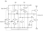
도 3은 본 발명의 실시예에 따른 시프트 레지스터의 블록 구성도.
도 4는 본 발명의 실시예에 따른 제N스테이지의 회로도.
도 5는 제N스테이지의 동작 파형을 나타난 도면.
도 6은 Q노드 전압 및 QB 노드 상의 전압을 나타나낸 파형도.
100A 표시영역
100B 비표시영역
110 타이밍 콘트롤러
120 데이터 구동부
130 레벨 시프터
130, 140 스캔 구동부
140 시프트 레지스터
Claims (9)
- 클럭신호들에 대응하여 스캔 신호를 시프트 하여 출력하는 복수의 스테이지들로 구성된 시프트 레지스터;를 포함하고,
상기 복수의 스테이지 중 제N 스테이지는,
Q 노드의 전압에 대응하여 제N 클럭신호를 출력 단자로 출력하는 풀업 트랜지스터;
QB 노드의 전압에 대응하여 저전위공급단자로부터의 저전위전압을 상기 출력 단자로 출력하는 풀다운 트랜지스터;
상기 Q노드의 전압에 의해 구동하여 고전위공급단자로부터의 고전위전압을 QH노드로 제공하는 제3 트랜지스터;
상기 QH 노드에 소스 전극이 연결되고, 상기 Q 노드에 드레인 전극이 연결되며, 상기 제N 스테이지의 다음 스테이지의 출력 단자에 게이트 전극이 연결된 제2-1 트랜지스터; 및
상기 QH 노드에 소스 전극이 연결되고, 상기 Q 노드에 드레인 전극이 연결되며, 상기 QB노드에 게이트 전극이 연결된 제4-1 트랜지스터;를 포함하는 스캔 구동부. - 제1 항에 있어서,
상기 제N 스테이지의 다음 스테이지의 출력 단자에 게이트 전극이 연결되고 상기 QH 노드에 드레인 전극이 연결되며 상기 저전위공급단자에 소스 전극이 연결된 제2-2 트랜지스터; 및
상기 QB 노드에 게이트 전극이 연결되고, 상기 QH 노드에 드레인 전극이 연결되며, 상기 저전위공급단자에 소스 전극이 연결된 제4-2 트랜지스터;를 더 포함하는 스캔 구동부. - 제2 항에 있어서,
상기 제N 스테이지의 이전 스테이지의 출력 단자에 게이트 전극이 연결되고, 상기 고전위전압을 상기 Q 노드로 제공하는 제1 트랜지스터; 및
상기 제N 스테이지의 이전 스테이지의 출력 단자에 게이트 전극이 연결되고, 상기 QB 노드로 상기 저전위전압을 제공하는 제10 트랜지스터;를 더 포함하는 스캔 구동부. - 제3 항에 있어서,
상기 QH 노드에 게이트 전극이 연결되고 상기 QB 노드에 상기 저전위전압을 제공하는 제6 트랜지스터;를 더 포함하는 스캔 구동부. - 제4 항에 있어서,
드레인 및 게이트 전극이 상기 고전위공급단자에 연결된 제7-1 트랜지스터;
상기 QH 노드에 게이트 전극이 연결되고, 상기 제7-1 트랜지스터의 소스 전극에 드레인 전극이 연결되며, 상기 저전위공급단자에 소스 전극이 연결된 제7-2 트랜지스터; 및
상기 제7-1 트랜지스터의 소스 전극에 게이트 전극이 연결되고, 상기 고전위전원공급단자와 상기 QB 노드 사이에 연결된 제5 트랜지스터;를 더 포함하는 스캔 구동부. - 제1 항에 있어서,
상기 Q 노드 전압이 제1 로우 레벨(Low level)에서 제1 하이 레벨(High level)로 변동 시 상기 QH 노드 전압은 제2 로우 레벨에서 제2 하이 레벨로 변동하고,
상기 Q 노드 전압이 상기 제1 하이 레벨로부터 변동된 제3 하이 레벨에서 상기 제1 로우 레벨로 변동 시 상기 QH 노드 전압은 제2 하이 레벨에서 제2 로우 레벨로 변동하는 스캔 구동부. - 제6 항에 있어서,
상기 QH 노드 전압은 상기 제2로우 레벨에서 상기 제1 로우 레벨로 변동하여 다시 제2 로우 레벨로 변동할 때까지 상기 Q노드 상의 전압의 최대 전압보다 낮은 전압을 유지하는 스캔 구동부. - 제5 항에 있어서,
상기 제2-1 트랜지스터 및 상기 제4-1 트랜지스터의 게이트 단자와 소스 단자 사이의 전압은 음의 값을 가지는 스캔 구동부. - 상기 제1 항에 따른 스캔 구동부; 및
상기 스캔 구동부에 연결된 복수의 스캔 라인을 포함하는 표시패널;을 포함하는 표시장치.
Priority Applications (1)
| Application Number | Priority Date | Filing Date | Title |
|---|---|---|---|
| KR1020140186165A KR102175905B1 (ko) | 2014-12-22 | 2014-12-22 | 스캔 구동부 및 이를 이용한 표시장치 |
Applications Claiming Priority (1)
| Application Number | Priority Date | Filing Date | Title |
|---|---|---|---|
| KR1020140186165A KR102175905B1 (ko) | 2014-12-22 | 2014-12-22 | 스캔 구동부 및 이를 이용한 표시장치 |
Publications (2)
| Publication Number | Publication Date |
|---|---|
| KR20160077315A true KR20160077315A (ko) | 2016-07-04 |
| KR102175905B1 KR102175905B1 (ko) | 2020-11-09 |
Family
ID=56500780
Family Applications (1)
| Application Number | Title | Priority Date | Filing Date |
|---|---|---|---|
| KR1020140186165A Active KR102175905B1 (ko) | 2014-12-22 | 2014-12-22 | 스캔 구동부 및 이를 이용한 표시장치 |
Country Status (1)
| Country | Link |
|---|---|
| KR (1) | KR102175905B1 (ko) |
Cited By (14)
| Publication number | Priority date | Publication date | Assignee | Title |
|---|---|---|---|---|
| KR20180055004A (ko) * | 2016-11-15 | 2018-05-25 | 엘지디스플레이 주식회사 | 표시패널과 이를 이용한 전계 발광 표시장치 |
| KR20180096843A (ko) * | 2017-02-20 | 2018-08-30 | 삼성디스플레이 주식회사 | 스테이지 회로 및 이를 이용한 주사 구동부 |
| WO2018201815A1 (zh) * | 2017-05-04 | 2018-11-08 | 京东方科技集团股份有限公司 | 移位寄存器及其驱动方法、栅极驱动电路和显示装置 |
| WO2018205322A1 (zh) * | 2017-05-12 | 2018-11-15 | 惠科股份有限公司 | 移位元暂存电路及其波形产生方法与其应用的显示面板 |
| CN109493783A (zh) * | 2018-12-21 | 2019-03-19 | 深圳市华星光电半导体显示技术有限公司 | Goa电路及显示面板 |
| KR20190036447A (ko) * | 2018-05-28 | 2019-04-04 | 엘지디스플레이 주식회사 | 표시패널과 이를 이용한 oled 표시 장치 |
| KR20190037860A (ko) * | 2017-09-29 | 2019-04-08 | 엘지디스플레이 주식회사 | 게이트 구동 회로 및 이를 구비한 평판 표시 장치 |
| KR20200020328A (ko) * | 2018-08-17 | 2020-02-26 | 엘지디스플레이 주식회사 | Oled 표시패널과 이를 이용한 oled 표시 장치 |
| US10957755B2 (en) | 2016-11-15 | 2021-03-23 | Lg Display Co., Ltd. | Display panel having a gate driving circuit arranged distributively in a display region of the display panel and organic light-emitting diode display device using the same |
| CN113436580A (zh) * | 2021-06-18 | 2021-09-24 | 武汉华星光电半导体显示技术有限公司 | 栅极驱动电路及显示面板 |
| KR20220095896A (ko) * | 2020-12-30 | 2022-07-07 | 엘지디스플레이 주식회사 | 게이트 구동부, 표시장치 및 이의 구동방법 |
| CN114999384A (zh) * | 2018-07-31 | 2022-09-02 | 乐金显示有限公司 | 栅极驱动器和使用栅极驱动器的电致发光显示装置 |
| US11735117B2 (en) | 2017-05-15 | 2023-08-22 | Samsung Display Co., Ltd. | Stage and scan driver using the same |
| WO2024020727A1 (zh) * | 2022-07-25 | 2024-02-01 | 京东方科技集团股份有限公司 | 移位寄存器单元、栅极驱动电路和栅极驱动方法 |
Citations (2)
| Publication number | Priority date | Publication date | Assignee | Title |
|---|---|---|---|---|
| KR20100083370A (ko) * | 2009-01-13 | 2010-07-22 | 삼성전자주식회사 | 게이트 구동회로 및 이를 갖는 표시장치 |
| KR20130115908A (ko) * | 2012-04-13 | 2013-10-22 | 엘지디스플레이 주식회사 | 표시장치 |
-
2014
- 2014-12-22 KR KR1020140186165A patent/KR102175905B1/ko active Active
Patent Citations (2)
| Publication number | Priority date | Publication date | Assignee | Title |
|---|---|---|---|---|
| KR20100083370A (ko) * | 2009-01-13 | 2010-07-22 | 삼성전자주식회사 | 게이트 구동회로 및 이를 갖는 표시장치 |
| KR20130115908A (ko) * | 2012-04-13 | 2013-10-22 | 엘지디스플레이 주식회사 | 표시장치 |
Cited By (23)
| Publication number | Priority date | Publication date | Assignee | Title |
|---|---|---|---|---|
| KR101878189B1 (ko) * | 2016-11-15 | 2018-07-16 | 엘지디스플레이 주식회사 | 표시패널과 이를 이용한 전계 발광 표시장치 |
| US11282428B2 (en) | 2016-11-15 | 2022-03-22 | Lg Display Co., Ltd. | Display panel including at least part of a gate driving circuit arranged in a display region, and organic light-emitting diode display device using the same |
| KR20180055004A (ko) * | 2016-11-15 | 2018-05-25 | 엘지디스플레이 주식회사 | 표시패널과 이를 이용한 전계 발광 표시장치 |
| US10957755B2 (en) | 2016-11-15 | 2021-03-23 | Lg Display Co., Ltd. | Display panel having a gate driving circuit arranged distributively in a display region of the display panel and organic light-emitting diode display device using the same |
| US10614732B2 (en) | 2017-02-20 | 2020-04-07 | Samsung Display Co., Ltd. | Stage circuit and scan driver using the same |
| KR20180096843A (ko) * | 2017-02-20 | 2018-08-30 | 삼성디스플레이 주식회사 | 스테이지 회로 및 이를 이용한 주사 구동부 |
| WO2018201815A1 (zh) * | 2017-05-04 | 2018-11-08 | 京东方科技集团股份有限公司 | 移位寄存器及其驱动方法、栅极驱动电路和显示装置 |
| US11120729B1 (en) | 2017-05-04 | 2021-09-14 | Boe Technology Group Co., Ltd. | Shift register, driving method thereof, gate driving circuit and display apparatus |
| WO2018205322A1 (zh) * | 2017-05-12 | 2018-11-15 | 惠科股份有限公司 | 移位元暂存电路及其波形产生方法与其应用的显示面板 |
| US10453412B2 (en) | 2017-05-12 | 2019-10-22 | HKC Corporation Limited | Shift register circuit, waveform generating method for same, and display panel using the same |
| US12236894B2 (en) | 2017-05-15 | 2025-02-25 | Samsung Display Co., Ltd. | Stage and scan driver using the same |
| US11735117B2 (en) | 2017-05-15 | 2023-08-22 | Samsung Display Co., Ltd. | Stage and scan driver using the same |
| KR20190037860A (ko) * | 2017-09-29 | 2019-04-08 | 엘지디스플레이 주식회사 | 게이트 구동 회로 및 이를 구비한 평판 표시 장치 |
| KR20190036447A (ko) * | 2018-05-28 | 2019-04-04 | 엘지디스플레이 주식회사 | 표시패널과 이를 이용한 oled 표시 장치 |
| CN114999384A (zh) * | 2018-07-31 | 2022-09-02 | 乐金显示有限公司 | 栅极驱动器和使用栅极驱动器的电致发光显示装置 |
| KR20200020328A (ko) * | 2018-08-17 | 2020-02-26 | 엘지디스플레이 주식회사 | Oled 표시패널과 이를 이용한 oled 표시 장치 |
| CN109493783A (zh) * | 2018-12-21 | 2019-03-19 | 深圳市华星光电半导体显示技术有限公司 | Goa电路及显示面板 |
| KR20220095896A (ko) * | 2020-12-30 | 2022-07-07 | 엘지디스플레이 주식회사 | 게이트 구동부, 표시장치 및 이의 구동방법 |
| WO2022262037A1 (zh) * | 2021-06-18 | 2022-12-22 | 武汉华星光电半导体显示技术有限公司 | 栅极驱动电路及显示面板 |
| US11955084B2 (en) | 2021-06-18 | 2024-04-09 | Wuhan China Star Optoelectronics Semiconductor Display Technology Co., Ltd. | Gate driver circuit and display panel |
| CN113436580A (zh) * | 2021-06-18 | 2021-09-24 | 武汉华星光电半导体显示技术有限公司 | 栅极驱动电路及显示面板 |
| WO2024020727A1 (zh) * | 2022-07-25 | 2024-02-01 | 京东方科技集团股份有限公司 | 移位寄存器单元、栅极驱动电路和栅极驱动方法 |
| US12614522B2 (en) | 2022-07-25 | 2026-04-28 | Hefei Boe Joint Technology Co., Ltd. | Shift register unit, gate driving circuit, and gate driving method |
Also Published As
| Publication number | Publication date |
|---|---|
| KR102175905B1 (ko) | 2020-11-09 |
Similar Documents
| Publication | Publication Date | Title |
|---|---|---|
| KR102175905B1 (ko) | 스캔 구동부 및 이를 이용한 표시장치 | |
| EP3029665B1 (en) | Display panel and method of driving the same | |
| US10078983B2 (en) | Scan driver, display device, and method of driving display device | |
| KR102656430B1 (ko) | 시프트 레지스터 및 이를 이용한 표시장치 | |
| CN108122523B (zh) | 栅极驱动电路和使用该栅极驱动电路的显示装置 | |
| KR101352289B1 (ko) | 표시장치 | |
| KR102020932B1 (ko) | 스캔 구동부 및 이를 이용한 표시장치 | |
| EP3330958B1 (en) | Display device having an integrated type scan driver | |
| KR20160000097A (ko) | 스캔 구동부 및 이를 이용한 표시장치 | |
| KR101366877B1 (ko) | 표시장치 | |
| KR20110102627A (ko) | 쉬프트 레지스터와 이를 이용한 표시장치 | |
| US11961480B2 (en) | Scan driver and organic light emitting display apparatus including the same | |
| KR102040659B1 (ko) | 스캔 구동부 및 이를 이용한 표시장치 | |
| KR102557841B1 (ko) | 게이트 구동회로와 이를 이용한 표시장치 | |
| KR102040650B1 (ko) | 스캔 구동부 및 이를 이용한 표시장치 | |
| KR20120044084A (ko) | 게이트 쉬프트 레지스터와 이를 이용한 표시장치 | |
| KR102051389B1 (ko) | 액정표시장치 및 이의 구동회로 | |
| KR20150086771A (ko) | 게이트 드라이버 및 그것을 포함하는 표시 장치 | |
| KR102222277B1 (ko) | 표시장치 | |
| KR101363194B1 (ko) | 표시장치 | |
| KR102634769B1 (ko) | 시프트 레지스터 및 이를 이용한 표시장치 | |
| KR102495831B1 (ko) | 게이트 구동부, 표시장치 및 이의 구동방법 | |
| KR102031365B1 (ko) | 스캔 구동부 및 이를 이용한 표시장치 | |
| KR102710414B1 (ko) | 게이트 구동회로와 이를 이용한 표시장치 | |
| KR101721260B1 (ko) | 레벨 쉬프터와 이를 이용한 표시장치 |
Legal Events
| Date | Code | Title | Description |
|---|---|---|---|
| PA0109 | Patent application |
St.27 status event code: A-0-1-A10-A12-nap-PA0109 |
|
| R17-X000 | Change to representative recorded |
St.27 status event code: A-3-3-R10-R17-oth-X000 |
|
| PG1501 | Laying open of application |
St.27 status event code: A-1-1-Q10-Q12-nap-PG1501 |
|
| R17-X000 | Change to representative recorded |
St.27 status event code: A-3-3-R10-R17-oth-X000 |
|
| P22-X000 | Classification modified |
St.27 status event code: A-2-2-P10-P22-nap-X000 |
|
| A201 | Request for examination | ||
| PA0201 | Request for examination |
St.27 status event code: A-1-2-D10-D11-exm-PA0201 |
|
| D13-X000 | Search requested |
St.27 status event code: A-1-2-D10-D13-srh-X000 |
|
| D14-X000 | Search report completed |
St.27 status event code: A-1-2-D10-D14-srh-X000 |
|
| E902 | Notification of reason for refusal | ||
| PE0902 | Notice of grounds for rejection |
St.27 status event code: A-1-2-D10-D21-exm-PE0902 |
|
| P22-X000 | Classification modified |
St.27 status event code: A-2-2-P10-P22-nap-X000 |
|
| E13-X000 | Pre-grant limitation requested |
St.27 status event code: A-2-3-E10-E13-lim-X000 |
|
| P11-X000 | Amendment of application requested |
St.27 status event code: A-2-2-P10-P11-nap-X000 |
|
| P13-X000 | Application amended |
St.27 status event code: A-2-2-P10-P13-nap-X000 |
|
| E701 | Decision to grant or registration of patent right | ||
| PE0701 | Decision of registration |
St.27 status event code: A-1-2-D10-D22-exm-PE0701 |
|
| GRNT | Written decision to grant | ||
| PR0701 | Registration of establishment |
St.27 status event code: A-2-4-F10-F11-exm-PR0701 |
|
| PR1002 | Payment of registration fee |
St.27 status event code: A-2-2-U10-U11-oth-PR1002 Fee payment year number: 1 |
|
| PG1601 | Publication of registration |
St.27 status event code: A-4-4-Q10-Q13-nap-PG1601 |
|
| PR1001 | Payment of annual fee |
St.27 status event code: A-4-4-U10-U11-oth-PR1001 Fee payment year number: 4 |
|
| PR1001 | Payment of annual fee |
St.27 status event code: A-4-4-U10-U11-oth-PR1001 Fee payment year number: 5 |
|
| PR1001 | Payment of annual fee |
St.27 status event code: A-4-4-U10-U11-oth-PR1001 Fee payment year number: 6 |
|
| U11 | Full renewal or maintenance fee paid |
Free format text: ST27 STATUS EVENT CODE: A-4-4-U10-U11-OTH-PR1001 (AS PROVIDED BY THE NATIONAL OFFICE) Year of fee payment: 6 |