KR20160090761A - Apparatus and method for dynamic control of plated uniformity with the use of remote electric current - Google Patents
Apparatus and method for dynamic control of plated uniformity with the use of remote electric current Download PDFInfo
- Publication number
- KR20160090761A KR20160090761A KR1020160007387A KR20160007387A KR20160090761A KR 20160090761 A KR20160090761 A KR 20160090761A KR 1020160007387 A KR1020160007387 A KR 1020160007387A KR 20160007387 A KR20160007387 A KR 20160007387A KR 20160090761 A KR20160090761 A KR 20160090761A
- Authority
- KR
- South Korea
- Prior art keywords
- ion
- anode
- substrate
- plating
- electroplating
- Prior art date
- Legal status (The legal status is an assumption and is not a legal conclusion. Google has not performed a legal analysis and makes no representation as to the accuracy of the status listed.)
- Granted
Links
Images





Classifications
-
- C—CHEMISTRY; METALLURGY
- C25—ELECTROLYTIC OR ELECTROPHORETIC PROCESSES; APPARATUS THEREFOR
- C25D—PROCESSES FOR THE ELECTROLYTIC OR ELECTROPHORETIC PRODUCTION OF COATINGS; ELECTROFORMING; APPARATUS THEREFOR
- C25D7/00—Electroplating characterised by the article coated
- C25D7/12—Semiconductors
-
- C—CHEMISTRY; METALLURGY
- C25—ELECTROLYTIC OR ELECTROPHORETIC PROCESSES; APPARATUS THEREFOR
- C25D—PROCESSES FOR THE ELECTROLYTIC OR ELECTROPHORETIC PRODUCTION OF COATINGS; ELECTROFORMING; APPARATUS THEREFOR
- C25D17/00—Constructional parts, or assemblies thereof, of cells for electrolytic coating
- C25D17/001—Apparatus specially adapted for electrolytic coating of wafers, e.g. semiconductors or solar cells
-
- C—CHEMISTRY; METALLURGY
- C25—ELECTROLYTIC OR ELECTROPHORETIC PROCESSES; APPARATUS THEREFOR
- C25D—PROCESSES FOR THE ELECTROLYTIC OR ELECTROPHORETIC PRODUCTION OF COATINGS; ELECTROFORMING; APPARATUS THEREFOR
- C25D5/00—Electroplating characterised by the process; Pretreatment or after-treatment of workpieces
- C25D5/04—Electroplating with moving electrodes
-
- C—CHEMISTRY; METALLURGY
- C25—ELECTROLYTIC OR ELECTROPHORETIC PROCESSES; APPARATUS THEREFOR
- C25D—PROCESSES FOR THE ELECTROLYTIC OR ELECTROPHORETIC PRODUCTION OF COATINGS; ELECTROFORMING; APPARATUS THEREFOR
- C25D17/00—Constructional parts, or assemblies thereof, of cells for electrolytic coating
- C25D17/002—Cell separation, e.g. membranes, diaphragms
-
- C—CHEMISTRY; METALLURGY
- C25—ELECTROLYTIC OR ELECTROPHORETIC PROCESSES; APPARATUS THEREFOR
- C25D—PROCESSES FOR THE ELECTROLYTIC OR ELECTROPHORETIC PRODUCTION OF COATINGS; ELECTROFORMING; APPARATUS THEREFOR
- C25D17/00—Constructional parts, or assemblies thereof, of cells for electrolytic coating
- C25D17/005—Contacting devices
-
- C—CHEMISTRY; METALLURGY
- C25—ELECTROLYTIC OR ELECTROPHORETIC PROCESSES; APPARATUS THEREFOR
- C25D—PROCESSES FOR THE ELECTROLYTIC OR ELECTROPHORETIC PRODUCTION OF COATINGS; ELECTROFORMING; APPARATUS THEREFOR
- C25D17/00—Constructional parts, or assemblies thereof, of cells for electrolytic coating
- C25D17/007—Current directing devices
-
- C—CHEMISTRY; METALLURGY
- C25—ELECTROLYTIC OR ELECTROPHORETIC PROCESSES; APPARATUS THEREFOR
- C25D—PROCESSES FOR THE ELECTROLYTIC OR ELECTROPHORETIC PRODUCTION OF COATINGS; ELECTROFORMING; APPARATUS THEREFOR
- C25D17/00—Constructional parts, or assemblies thereof, of cells for electrolytic coating
- C25D17/008—Current shielding devices
-
- C—CHEMISTRY; METALLURGY
- C25—ELECTROLYTIC OR ELECTROPHORETIC PROCESSES; APPARATUS THEREFOR
- C25D—PROCESSES FOR THE ELECTROLYTIC OR ELECTROPHORETIC PRODUCTION OF COATINGS; ELECTROFORMING; APPARATUS THEREFOR
- C25D17/00—Constructional parts, or assemblies thereof, of cells for electrolytic coating
- C25D17/06—Suspending or supporting devices for articles to be coated
-
- C—CHEMISTRY; METALLURGY
- C25—ELECTROLYTIC OR ELECTROPHORETIC PROCESSES; APPARATUS THEREFOR
- C25D—PROCESSES FOR THE ELECTROLYTIC OR ELECTROPHORETIC PRODUCTION OF COATINGS; ELECTROFORMING; APPARATUS THEREFOR
- C25D17/00—Constructional parts, or assemblies thereof, of cells for electrolytic coating
- C25D17/10—Electrodes, e.g. composition, counter electrode
-
- C—CHEMISTRY; METALLURGY
- C25—ELECTROLYTIC OR ELECTROPHORETIC PROCESSES; APPARATUS THEREFOR
- C25D—PROCESSES FOR THE ELECTROLYTIC OR ELECTROPHORETIC PRODUCTION OF COATINGS; ELECTROFORMING; APPARATUS THEREFOR
- C25D17/00—Constructional parts, or assemblies thereof, of cells for electrolytic coating
- C25D17/10—Electrodes, e.g. composition, counter electrode
- C25D17/12—Shape or form
-
- C—CHEMISTRY; METALLURGY
- C25—ELECTROLYTIC OR ELECTROPHORETIC PROCESSES; APPARATUS THEREFOR
- C25D—PROCESSES FOR THE ELECTROLYTIC OR ELECTROPHORETIC PRODUCTION OF COATINGS; ELECTROFORMING; APPARATUS THEREFOR
- C25D21/00—Processes for servicing or operating cells for electrolytic coating
- C25D21/12—Process control or regulation
-
- C—CHEMISTRY; METALLURGY
- C25—ELECTROLYTIC OR ELECTROPHORETIC PROCESSES; APPARATUS THEREFOR
- C25D—PROCESSES FOR THE ELECTROLYTIC OR ELECTROPHORETIC PRODUCTION OF COATINGS; ELECTROFORMING; APPARATUS THEREFOR
- C25D7/00—Electroplating characterised by the article coated
- C25D7/06—Wires; Strips; Foils
- C25D7/0614—Strips or foils
-
- C—CHEMISTRY; METALLURGY
- C25—ELECTROLYTIC OR ELECTROPHORETIC PROCESSES; APPARATUS THEREFOR
- C25F—PROCESSES FOR THE ELECTROLYTIC REMOVAL OF MATERIALS FROM OBJECTS; APPARATUS THEREFOR
- C25F5/00—Electrolytic stripping of metallic layers or coatings
-
- C—CHEMISTRY; METALLURGY
- C25—ELECTROLYTIC OR ELECTROPHORETIC PROCESSES; APPARATUS THEREFOR
- C25D—PROCESSES FOR THE ELECTROLYTIC OR ELECTROPHORETIC PRODUCTION OF COATINGS; ELECTROFORMING; APPARATUS THEREFOR
- C25D7/00—Electroplating characterised by the article coated
- C25D7/12—Semiconductors
- C25D7/123—Semiconductors first coated with a seed layer or a conductive layer
Landscapes
- Chemical & Material Sciences (AREA)
- Engineering & Computer Science (AREA)
- Chemical Kinetics & Catalysis (AREA)
- Electrochemistry (AREA)
- Materials Engineering (AREA)
- Metallurgy (AREA)
- Organic Chemistry (AREA)
- Life Sciences & Earth Sciences (AREA)
- Sustainable Development (AREA)
- Electroplating Methods And Accessories (AREA)
- Electrodes Of Semiconductors (AREA)
- Automation & Control Theory (AREA)
Abstract
Description
본 개시물은 일반적으로 반도체 웨이퍼 상에 금속 층을 전기도금하기 위한 방법 및 장치에 관한 것이다. 더 구체적으로, 본 명세서에 기술된 방법 및 장치는 도금 균일도를 제어하는데 유용하다.The present disclosure generally relates to methods and apparatus for electroplating metal layers on semiconductor wafers. More specifically, the methods and apparatus described herein are useful for controlling plating uniformity.
집적 회로 (IC) 제조에서 알루미늄으로부터 구리로의 전이는 프로세스 "아키텍처"의 변화 (다마신 (damascene) 및 듀얼-다마신으로) 뿐만 아니라 완전히 새로운 프로세스 기술들의 세트를 요구한다. 구리 다마신 회로들을 생성하는데 사용되는 일 프로세스 단계는 상부에 구리가 전기도금되는 ("전해 충진 (electrofill)") 기저 층으로서 사용되는, "씨드층" 또는 "스트라이크층"의 형성이다. 씨드층은 전기 도금 전류를 (전기 콘택트가 이루어지는) 웨이퍼의 에지 구역으로부터 웨이퍼 표면에 걸쳐 위치된 모든 트렌치들 및 비아 구조체들로 운반한다. 다른 전도성 재료들이 애플리케이션에 따라 사용될 수 있지만, 씨드 막은 통상적으로 얇은 전도성 구리 층이다. 씨드 막은 배리어 층에 의해 절연 실리콘 다이옥사이드 또는 다른 유전체로부터 분리된다. 씨드 층 증착 프로세스는 양호한 전반적인 접착력, 우수한 단차 커버리지 (보다 구체적으로, 금속의 컨포멀하고 (conformal) 연속적인 층들이 임베딩된 (embedded) 리세스된 피처의 측벽들 상에 증착되어야 함), 및 임베딩된 리세스된 피처의 상단의 최소 폐쇄 또는 "넥킹 (necking)" 을 가진 층을 산출해야 한다. The transition from aluminum to copper in integrated circuit (IC) manufacturing requires a whole new set of process technologies as well as changes in the process "architecture" (with damascene and dual-damascene). One process step used to create copper damascene circuits is the formation of a "seed layer" or "strike layer ", which is used as a base layer in which copper is electroplated on top (" electrofill " The seed layer carries an electroplating current to all the trenches and via structures located across the wafer surface from the edge region of the wafer (where electrical contact is made). While other conductive materials may be used depending on the application, the seed film is typically a thin conductive copper layer. The seed layer is separated from the insulating silicon dioxide or other dielectric by the barrier layer. The seed layer deposition process requires good overall adhesion, excellent step coverage (more specifically, it must be deposited on the sidewalls of the recessed features embedded in conformal continuous layers of metal), and embedding Quot; necking "at the top of the recessed features.
점점 더 보다 작은 피처들의 시장 동향들 및 대안적인 씨드 프로세스들은 점점 더 얇은 씨드 층들 상에 높은 정도의 균일도로 도금하는 능력을 필요로 한다. 미래에는, 씨드 막이 단순히 (예를 들어, 원자 층 증착 (ALD) 또는 유사한 프로세스에 의해 증착된) 구리 및 매우 얇은 배리어의 바이레이어 (bilayer) 또는 루테늄과 같은, 도금 가능한 (plateable) 배리어 막으로 이루어질 수도 있다는 것이 예상된다. 이러한 맴브레인들은 엔지니어가 심각한 터미널 효과 (terminal effect) 상황을 겪게한다. 예를 들어, 3 암페어의 총 전류를 정사각형 루테늄 씨드 층 (30 내지 50 Å 막에 대한 적당한 값) 당 30 ohm 내로 균일하게 흘릴 때, 금속 내에서 발생한 중심 대 에지 (방사상) 전압 강하는 2 볼트 이상일 것이다. 큰 표면적을 효과적으로 도금하기 위해서, 도금 툴은 웨이퍼 기판의 에지 구역 내에서만 전도성 씨드에 전기적으로 콘택트한다. 기판의 중심 구역에 대한 직접적인 콘택트는 없다. 따라서, 매우 저항성인 씨드 층들에 대해, 층의 에지에서의 전위는 층의 중심 구역에서보다 보다 상당히 크다. 저항 및 전압 보상의 적절한 수단 없이, 이 큰 에지-대-중심 전압 강하는 주로 웨이퍼 에지에서의 보다 두꺼운 도금에서 특징으로 하는, 극도로 불균일한 도금 레이트 및 불균일한 도금 두께 분포를 야기할 수 있다. 이 도금 불균일도는 방사상 불균일도, 즉, 원형 웨이퍼의 반경을 따르는 균일도 변동이다.Market trends of increasingly smaller features and alternative seed processes require the ability to plate with increasingly uniform uniformity over increasingly thin seed layers. In the future, the seed film may be made of a plate-like barrier film, such as bilayer or ruthenium, of copper and a very thin barrier (e. G., Deposited by atomic layer deposition (ALD) It is expected that it may be. These membranes cause engineers to experience severe terminal effects. For example, when the total current of 3 amperes flows uniformly within 30 ohms per square ruthenium seed layer (suitable for 30 to 50 占 film), the center-to-edge (radial) voltage drop that occurs in the metal is greater than 2 volts will be. In order to effectively coat a large surface area, the plating tool electrically contacts the conductive seed only within the edge region of the wafer substrate. There is no direct contact to the central region of the substrate. Thus, for highly resistant seed layers, the potential at the edge of the layer is significantly greater than at the center region of the layer. Without adequate means of resistance and voltage compensation, this large edge-to-center voltage drop can result in an extremely non-uniform plating rate and a non-uniform plating thickness distribution, which is characterized mainly by thicker plating at the wafer edge. This plating non-uniformity is radial non-uniformity, i. E. Uniformity variation along the radius of the circular wafer.
완화되어야 하는 또 다른 타입의 불균일도는 방위각 불균일도이다. 명료성을 위해, 우리는 두께 변동들이 웨이퍼 중심으로부터 고정된 방사상 위치에서 워크피스 상의 상이한 각 위치들에서 나타나기 때문에, 극 좌표들을 사용하여, 방위각 불균일도, 즉, 웨이퍼의 주변 내의 원형의 부분 또는 주어진 원형을 따른 불균일도를 규정한다. 이 타입의 불균일도는 방사상 불균일도와 관계없이 전기도금 애플리케이션들에서 존재할 수 있고, 일부 애플리케이션들에서 제어될 필요가 있는 불균일도의 주된 타입일 수도 있다. 이 타입의 불균일도는 종종 웨이퍼의 주요한 부분이 포토레지스트 코팅 또는 유사한 도금-방지 층으로 마스킹되는 경우에 레지스트 도금을 통해 발생하고, 피처들 또는 피처 밀도들의 마스킹된 패턴은 웨이퍼 에지 근방에서 방위각으로 균일하지 않다. 예를 들어, 일부 경우들에서 웨이퍼 넘버링 또는 핸들링을 허용하도록 웨이퍼의 노치 근방의 없어진 패턴 피처들의 기술적으로 요구된 익현 (chord) 구역이 있을 수도 있다. 없어진 구역 내부의 방사상으로 그리고 방위각으로 가변 가능한 도금 레이트들은 칩 다이로 하여금 비-기능적으로 되게 할 수도 있고, 그러므로 이 상황을 피하기 위한 방법들 및 장치가 필요하다.Another type of non-uniformity that needs to be mitigated is azimuth non-uniformity. For the sake of clarity, we use azimuthal azimuths, i.e., the portion of the circle in the periphery of the wafer, or the radius of the circle in the periphery of the wafer, because the thickness variations appear at different angular positions on the workpiece at fixed radial positions from the wafer center. And the like. This type of non-uniformity may be present in electroplating applications irrespective of radial nonuniformity, and may be the main type of non-uniformity that needs to be controlled in some applications. This type of non-uniformity often occurs through resist plating when a major portion of the wafer is masked with a photoresist coating or similar anti-deposit layer, and the masked pattern of features or feature densities is uniformly azimuthally near the wafer edge I do not. For example, there may be a technically required chord region of missing pattern features near the notch of the wafer to permit wafer numbering or handling in some cases. Plating rates that are radially and azimuthally variable within a missing area may cause the chip die to become non-functional, and therefore methods and apparatus are needed to avoid this situation.
이제 전기 화학 증착은 WLP (wafer level packaging) 및 TSV (through silicon via) 전기 연결 기술로서 일반적으로 공지된 멀티칩 상호접속 기술들 및 정교한 패키징에 대한 상업적 필요를 충족시키도록 준비된다. 이들 기술들은 기술들 자체의 매우 상당한 과제들을 나타낸다.Electrochemical deposition is now being prepared to meet the commercial needs for commonly known multi-chip interconnect technologies and sophisticated packaging as wafer level packaging (WLP) and through silicon via (TSV) electrical interconnect technologies. These techniques represent very significant challenges in the technologies themselves.
일반적으로, TSV를 생성하는 프로세스들은 다마신 프로세싱과 대략 유사하지만 상이한 보다 큰 사이즈 스케일에서 실시되고 보다 고 종횡비 리세스된 피처들을 활용한다. TSV 프로세싱에서 캐비티 또는 리세스는 유전체 층 (예를 들어 실리콘 다이옥사이드 층) 내로 먼저 에칭되고; 이어서 리세스된 피처의 내부의 표면과 기판의 필드 구역 양자는 확산 배리어 및/또는 접착 (스틱 (stick)) 층 (예를 들어 Ta, Ti, TiW, TiN, TaN, Ru, Co, Ni, W), 및 "전기도금 가능한 씨드 층" (예를 들어 물리적 기상 증착 (PVD) 프로세스, 화학적 기상 증착 (CVD) 프로세스, ALD 프로세스, 또는 무전해 도금 프로세스에 의해 증착될 수 있는 예를 들어 Cu, Ru, Ni, Co) 으로 금속화된다. 다음에, 금속화된 리세스된 피처들은 예를 들어, "상향식" 구리 전기도금을 사용하여, 금속으로 충진된다. 대조적으로, 쓰루 레지스트 WLP 피처 형성은 통상적으로 상이하게 진행된다. 프로세스는 통상적으로 일부 저 종횡비 비아들 또는 패드들을 포함할 수도 있는 실질적으로 평면인 기판을 사용하여 시작된다. 실질적으로 평면인 유전체 기판은 접착 층, 이어서 (통상적으로 PVD에 의해 증착된) 씨드 층으로 코팅된다. 이어서 씨드 층이 노출되는 도금-마스킹 포토레지스트 없이, 개방 영역들의 패턴을 생성하도록 씨드 층 위에 포토레지스트 층이 증착되고, 패터닝된다. 다음에, 금속은 포토레지스트를 벗긴 후, 및 에칭에 의한 씨드 층의 제거 후, 기판 위에 다양한 전기적으로 절연된 올록볼록한 구조체들을 남기는 기판 상에 필라 (pillar), 라인, 또는 또 다른 피처를 형성하도록 개방 영역들 내로 전기도금된다.Generally, the processes for generating the TSV are similar to the damascene processing, but are performed on different larger size scales and utilize the higher aspect ratio recessed features. In TSV processing, the cavity or recess is first etched into a dielectric layer (e.g., a silicon dioxide layer); Both the interior surface of the recessed features and the field areas of the substrate are then subjected to diffusion barrier and / or adhesion (stick) layers (e.g., Ta, Ti, TiW, TiN, TaN, Ru, ), Which can be deposited by an electroless plating process, an " electroplated seed layer "(e.g., a physical vapor deposition (PVD) process, a chemical vapor deposition (CVD) process, an ALD process, , Ni, Co). The metallized recessed features are then filled with metal, for example, using "bottom-up" copper electroplating. In contrast, through resist WLP feature formation typically proceeds differently. The process begins with a substantially planar substrate, which may typically include some low aspect ratio vias or pads. A substantially planar dielectric substrate is coated with an adhesive layer followed by a seed layer (typically deposited by PVD). A photoresist layer is then deposited and patterned over the seed layer to produce a pattern of open areas, without a plating-masking photoresist where the seed layer is exposed. The metal may then be patterned to form a pillar, line, or other feature on the substrate leaving the various electrically isolated, convex structures on the substrate after the photoresist is stripped and after removal of the seed layer by etching Electroplated into the open areas.
이들 기술들 (TSV 및 쓰루 레지스트 도금) 양자는 다마신 애플리케이션들보다 상당히 보다 큰 사이즈의 스케일의 전기도금을 필요로 한다. 패키징 피처들 (예를 들어 쓰루 칩 연결 TSV, 상호접속 재분포 배선, 또는 보드 또는 칩에 대한 칩 결합, 예를 들어, 플립-칩 필라들) 의 타입 및 애플리케이션에 따라, 도금된 피처들은 보통 현재 기술에서, 직경에 있어서 약 2 마이크로미터 초과이고 통상적으로 직경에 있어서 5 내지 100 마이크로미터이다 (예를 들어, 필라들은 직경에 있어서 약 50 마이크로미터일 수도 있음). 전력 버스들과 같은 일부 온-칩 (on-chip) 구조체들에 대해, 도금될 피처는 100 마이크로미터보다 보다 클 수도 있다. 쓰루 레지스트 WLP 피처들의 종횡비들은 통상적으로 약 2:1 (높이 대 폭) 이하이고, 보다 통상적으로 1:1 이하이고, 반면에 TSV 구조체들은 매우 높은 종횡비들 (예를 들어, 약 10:1 또는 20:1) 을 가질 수 있다.Both of these techniques (TSV and through resist plating) require electroplating of scales of significantly larger size than damascene applications. Depending on the type and application of the packaging features (e.g., through-chip connection TSV, interconnect redistribution wiring, or chip combination for the board or chip, for example, flip-chip pillars) (For example, the pillars may be about 50 micrometers in diameter), which is about 2 micrometers in diameter and typically 5 to 100 micrometers in diameter. For some on-chip structures, such as power busses, the features to be plated may be greater than 100 micrometers. The aspect ratios of through resist WLP features are typically less than or equal to about 2: 1 (height to width) and more typically less than or equal to 1: 1, while TSV structures have very high aspect ratios (e.g., about 10: 1 or 20 : 1).
상대적으로 많은 양의 증착될 재료를 고려해 볼 때, 피처 사이즈뿐만 아니라 도금 속도는 다마신 애플리케이션들로부터 WLP 애플리케이션 및 TSV 애플리케이션을 구별한다. 많은 WLP 애플리케이션들에 대해, 도금은 적어도 약 2 마이크로미터/분, 및 통상적으로 적어도 약 4 마이크로미터/분의 레이트로, 그리고 일부 애플리케이션들에 대해 적어도 약 7 마이크로미터/분의 레이트로 피처들을 충진해야 한다. 실제 레이트들은 증착되는 특정한 금속에 따라 가변할 것이다. 하지만 이들 보다 고 도금 레이트 레짐들 (regimes) 에서, 도금 표면으로의 전해액 내의 금속 이온들의 효율적인 대량 전달 (mass transfer) 은 매우 중요하다. 보다 고 도금 레이트들은 적합한 피처 형상을 유지하는 것뿐만 아니라 다이 및 웨이퍼 스케일 두께 균일도를 제어하는 것에 관하여 수많은 과제들을 야기한다. Considering the relatively large amount of material to be deposited, the feature size as well as the plating rate distinguish WLP applications and TSV applications from damascene applications. For many WLP applications, the plating may fill the features at a rate of at least about 2 micrometers per minute, and typically at least about 4 micrometers per minute, and at a rate of at least about 7 micrometers per minute for some applications Should be. The actual rates will vary depending on the particular metal being deposited. However, at higher plating rate regimes, efficient mass transfer of metal ions in the electrolyte to the plating surface is very important. Higher plating rates cause numerous challenges with respect to controlling die and wafer scale thickness uniformity as well as maintaining the proper feature shape.
또 다른 균일도 제어 과제는 일 전기도금 툴 내에서 연속적으로 프로세싱될 필요가 있을 수도 있는 이종 기판들에 의해 야기된다. 예를 들어, 상이한 생성물을 위해 각각 타깃된 2개의 상이한 반도체 프로세스-내 웨이퍼들은, 반도체 웨이퍼의 에지 구역 근방의 리세스된 피처들의 실질적으로 상이한 방사상 분포를 가질 수도 있고, 그러므로 양자를 위해 목표된 균일도를 달성하도록 상이한 보상들을 요구할 것이다. 따라서, 우수한 도금 균일도 및 최소 도금 툴 다운시간으로 이종 기판들을 연속적으로 프로세싱할 수 있을 전기도금 장치가 필요하다.Another uniformity control problem is caused by heterogeneous substrates that may need to be continuously processed within a single electroplating tool. For example, two different semiconductor process-in-wafers, each targeted for a different product, may have a substantially different radial distribution of recessed features in the vicinity of the edge region of the semiconductor wafer, and therefore the desired uniformity Lt; / RTI > Therefore, there is a need for an electroplating apparatus that is capable of continuously processing dissimilar substrates with good plating uniformity and minimum plating tool down time.
방사상 불균일도, 방위각 불균일도 또는 양자와 같은, 도금 불균일도를 제어하면서 기판 상에 금속을 전기도금하기 위한 방법 및 장치가 기술된다. 본 명세서에 기술된 장치 및 방법들은 TSV 또는 WLP 리세스된 피처들을 가진 반도체 웨이퍼 기판들을 포함하는 다양한 기판들 상에서 전기도금하기 위해 사용될 수 있다. 장치 및 방법들은 장치가 방사상 및/또는 방위각 균일도 제어를 허용하도록 설계되고 하드웨어 변화들 없이 기판들에서 광범위한 차이들을 수용할 수 있기 때문에, 이종 기판들 상의 금속의 순차적인 도금을 위해 특히 유용하다. 그러므로, 이종 기판들을 프로세싱하는 전기도금 툴의 다운시간은 실질적으로 감소될 수 있다.A method and apparatus for electroplating metal on a substrate while controlling the plating non-uniformity, such as radial non-uniformity, azimuthal non-uniformity, or both, is described. The devices and methods described herein can be used for electroplating on a variety of substrates including semiconductor wafer substrates with TSV or WLP recessed features. The apparatus and methods are particularly useful for sequential plating of metals on heterogeneous substrates because the apparatus is designed to allow radial and / or azimuthal uniformity control and can accommodate a wide variety of differences in substrates without hardware variations. Therefore, the downtime of the electroplating tool for processing heterogeneous substrates can be substantially reduced.
발명의 제 1 양태에서, 기판 상에 금속을 전기도금하기 위한 전기도금 장치가 제공되고, 장치는: (a) 전해액 (금속 이온들 및 보통 산을 포함함) 을 포함하도록 구성된 도금 챔버로서, 도금 챔버는 캐소드액 격실 및 애노드액 격실을 포함하고, 애노드액 격실 및 캐소드액 격실은 이온-투과성 맴브레인 (일부 실시예들에서 맴브레인은 기전력 하에서 애노드액으로부터 캐소드액으로 맴브레인을 통해 금속 이온 이동을 허용하지만, 맴브레인을 걸친 전해액 플로우 및 금속 이온 대류적 이동을 실질적으로 방지함) 에 의해 분리되는, 도금 챔버; (b) 전기도금 동안 캐소드액 격실 내에서 기판을 홀딩하고 회전시키도록 구성된 기판 홀더; (c) 도금 챔버의 애노드액 격실 내에 배치된 1차 애노드; (d) 이온-투과성 맴브레인과 기판 홀더 사이에 배치된 이온 저항성 이온 투과성 엘리먼트로서, 전기도금 동안 엘리먼트를 통해 이온 이송을 제공하도록 구성되는, 이온 저항성 이온 투과성 엘리먼트; 및 (e) 기판의 대략적인 주변으로 도금 전류 (또한 여기서 이온 전류로 지칭됨) 를 공여하고 (donate) 그리고/또는 기판의 대략적인 주변으로부터의 도금 전류를 방향 전환하도록 구성된 2차 전극으로서, 2차 전극은 공여되고 그리고/또는 방향 전환된 도금 전류가 애노드액 격실 및 캐소드액 격실을 분리하는 이온-투과성 맴브레인을 넘어가지 않도록 배치되고, 2차 전극은 이온 저항성 이온 투과성 엘리먼트를 통해 도금 전류를 공여하고 그리고/또는 방향 전환하도록 배치되는, 2차 전극을 포함한다.In a first aspect of the invention, there is provided an electroplating apparatus for electroplating metal on a substrate, the apparatus comprising: (a) a plating chamber configured to include an electrolyte (including metal ions and usually an acid) The chamber includes a cathode liquid compartment and an anode liquid compartment, wherein the anode liquid compartment and the cathode liquid compartment are ion-permeable membranes (in some embodiments, the membranes allow metal ion transfer through the membrane from the anode liquid to the cathode liquid under electromotive force , Substantially preventing electrolytic flow and metal ion convective migration across the membrane); (b) a substrate holder configured to hold and rotate the substrate in the cathode liquid compartment during electroplating; (c) a primary anode disposed in the anode liquid compartment of the plating chamber; (d) an ion-resistant ion-permeable element disposed between the ion-permeable membrane and the substrate holder, the ion-resistant ion-permeable element being configured to provide ion transport through the element during electroplating; And (e) a secondary electrode configured to donate a plating current (also referred to herein as an ion current) to the approximate periphery of the substrate and / or to divert the plating current from the approximate periphery of the substrate, The secondary electrode is disposed such that the donor and / or redirected plating current does not cross the ion-permeable membrane separating the anode liquid compartment and the cathode liquid compartment, and the secondary electrode donates the plating current through the ion- And / or are arranged to redirect and / or redirect.
일부 실시예들에서 2차 전극은 기판으로 도금 전류를 공여하도록 구성된 방위각으로 대칭인 애노드이다. 예를 들어, 2차 애노드는 일반적으로 환형 형상을 가질 수도 있다. 2차 애노드는 불활성 애노드 또는 소모성 (활성의) 애노드 (예를 들어, 구리를 포함하는 소모성 애노드) 일 수도 있다. 일부 실시예들에서 2차 애노드는 도금 챔버의 주변 둘레에서, 2차 애노드 실 내에 배치될 수도 있고, 2차 애노드 실은 이온-투과성 맴브레인에 의해 캐소드액 격실로부터 분리될 수도 있다. 다른 실시예들에서, 캐소드액으로부터 그리고 기판으로부터 2차 애노드를 분리하기 위한 맴브레인은 사용되지 않는다. 일부 실시예들에서 장치는 2차 애노드 실 내에서 2차 애노드를 세척하기 (irrigate) 위한 하나 이상의 채널들을 포함한다. 일부 실시예들에서 장치는 2차 애노드 실로부터 버블들을 수집하고 제거하기 위한 하나 이상의 채널들을 포함한다. 장치는 전기도금 동안 2차 애노드를 동적으로 제어하도록 구성될 수도 있다.In some embodiments, the secondary electrode is an azimuthally symmetric anode configured to donate plating current to the substrate. For example, the secondary anode may have a generally annular shape. The secondary anode may be an inert anode or a consumable (active) anode (e.g., a consumable anode comprising copper). In some embodiments, the secondary anode may be disposed in the secondary anode chamber, around the periphery of the plating chamber, and the secondary anode chamber may be separated from the cathode liquid compartment by an ion-permeable membrane. In other embodiments, the membrane for separating the secondary anode from the cathode solution and from the substrate is not used. In some embodiments, the apparatus includes one or more channels for irrigating the secondary anode in the secondary anode chamber. In some embodiments, the apparatus includes one or more channels for collecting and removing bubbles from the secondary anode chamber. The apparatus may be configured to dynamically control the secondary anode during electroplating.
일부 실시예들에서 1차 애노드는 기판의 도금 면의 직경 또는 폭보다 보다 작은 직경 또는 폭을 갖도록 장치가 설계된다. 이 설계에서 1차 애노드를 하우징하는 도금 챔버의 일부분은 기판의 도금 면의 직경 또는 폭보다 보다 작은 직경 또는 폭을 가질 수도 있다.In some embodiments, the device is designed such that the primary anode has a diameter or width less than the diameter or width of the plating surface of the substrate. In this design, a portion of the plating chamber housing the primary anode may have a smaller diameter or width than the diameter or width of the plating surface of the substrate.
장치의 일부 실시예들에서 이온 저항성 이온 투과성 엘리먼트는 적어도 3개의 부분들: (a) 외측 이온 투과성 부분; (b) 중간의, 이온 불투과성 부분; 및 (c) 내측 이온 투과성 부분을 포함하고, 장치는 2차 애노드로부터 내측 이온 투과성 부분이 아닌, 외측 이온 투과성 부분을 통해 도금 전류를 공여하도록 구성된다. 일부 실시예들에서 이온 저항성 이온 투과성 엘리먼트의 중간의, 이온 불투과성 부분은 엘리먼트의 반대 측면 상에서보다 기판에 가장 가까운 이온 저항성 이온 투과성 엘리먼트의 표면 상에서 보다 작도록 형성된다. 일부 실시예들에서, 이온 저항성 이온 투과성 엘리먼트의 중간의, 이온 불투과성 부분은, 기판과 대면하는 이온 저항성 이온 투과성 엘리먼트의 표면 상의 채널 개구들이 이온 저항성 이온 투과성 엘리먼트의 반경을 따라 실질적으로 균일하게 분포되고, 그리고 외측 부분 및 중심 부분의 채널 개구들 사이의 가장 가까운 평균 거리보다 보다 큰 이온 불투과성 부분이 있기 위해 기판에 반대되는 이온 저항성 이온 투과성 엘리먼트의 표면 상의 채널 개구들이 분포되도록, 내측 부분과 외측 부분의 채널들 사이에 형성되고, 이 이온 불투과성 부분은 이온 저항성 이온 투과성 엘리먼트의 중간의 이온 불투과성 부분에 대응한다.In some embodiments of the apparatus, the ion-resistant ion-permeable element comprises at least three portions: (a) an outer ion-permeable portion; (b) an intermediate, ion impermeable portion; And (c) an inner ion permeable portion, wherein the device is configured to donate plating current through an outer ion permeable portion, rather than an inner ion permeable portion, from the secondary anode. In some embodiments, the intermediate, impermeable portion of the ion-resistant ion-permeable element is formed to be smaller on the surface of the ion-resistant ion-permeable element closest to the substrate than on the opposite side of the element. In some embodiments, the ion-impermeable portion, intermediate the ion-resistant ion-permeable element, has channel openings on the surface of the ion-resistant ion-permeable element facing the substrate substantially uniformly distributed along the radius of the ion- And the channel openings on the surface of the ion-resistant ion-permeable element opposite to the substrate are distributed so that there is a larger ion-impermeable portion than the nearest average distance between the channel portions of the outer portion and the central portion, And the ion-impermeable portion corresponds to an ion-impermeable portion in the middle of the ion-resistant ion-permeable element.
증착 동안, 이온 저항성 이온 투과성 엘리먼트는 기판에 아주 근접하여 바람직하게 배치되고, 통상적으로 10 ㎜ 이하의 갭에 의해 기판의 도금 표면으로부터 분리되고, 보다 작은 갭들 (예를 들어 5 ㎜ 이하) 은 보다 작은 기판들 (예를 들어 300 ㎜ 직경 웨이퍼들) 을 프로세싱하는 장치들에서 바람직하고 보다 큰 갭들은 보다 큰 기판들 (예를 들어 450 ㎜ 이상의 직경을 가진 웨이퍼들) 을 프로세싱하기 위해 구성된 장치들에서 유용하다. 기판 직경 대 통상적으로 기판의 도금 가능한 표면과 이온 저항성 이온 투과성 엘리먼트의 가장 가까운 표면 사이의 갭의 사이즈의 무차원 비 (dimensionless ratio) 는 약 30:1 초과이어야 한다. 일부 실시예들에서 장치는 갭으로 흐르는 전해액을 도입하기 위한 갭에 대한 유입부 및 갭을 통해 흐르는 전해액을 수용하기 위한 갭에 대한 유출부를 더 포함하고, 유입부 및 유출부는 기판의 도금 면의 방위각으로 반대되는 주변 위치들에 근접하게 배치되고, 유입부 및 유출부는 갭에서 전해액의 크로스-플로우를 생성하도록 구성된다.During deposition, the ion-resistant ion-permeable element is preferably disposed in close proximity to the substrate and is typically separated from the plating surface of the substrate by a gap of 10 mm or less, and smaller gaps (e.g., 5 mm or less) In devices that process substrates (e.g., 300 mm diameter wafers), preferred and larger gaps are useful in devices configured for processing larger substrates (e.g., wafers having a diameter of 450 mm or more) Do. The dimensionless ratio of the size of the substrate to the gap typically between the platable surface of the substrate and the nearest surface of the ion-resistant ion-permeable element should be greater than about 30: 1. In some embodiments, the apparatus further comprises an inlet for a gap for introducing the electrolyte flowing into the gap and an outlet for a gap for receiving the electrolyte flowing through the gap, wherein the inlet and outlet are configured such that the azimuth angle And the inlet and outlet are configured to produce a cross-flow of the electrolyte in the gap.
일부 실시예들에서 (예를 들어, 2차 전극이 방위각으로 비대칭인 전극 또는 방위각 불균일도를 정정하도록 구성된 세그먼트화된 (segmented) 전극일 때), 장치는 방위각 균일도를 부가적으로 제어하기 위해 구성된 3차 전극을 더 포함할 수도 있고, 3차 전극은 애노드, 캐소드 및 애노드-캐소드로 구성된 그룹으로부터 선택되고, 그리고 3차 전극은 동일한 평균 호 길이 및 동일한 평균 방사상 위치를 갖고 상이한 방위각 각 위치에 있는 기판의 제 2 부분과 상이하게 기판의 선택된 방위각 위치에서의 기판의 제 1 (방위각) 부분으로 도금 전류를 공여하고 그리고/또는 방향 전환하도록 구성된 방위각으로 비대칭이거나 멀티-세그먼트화된 전극이다. 일부 실시예들에서 3차 전극은 기판으로 도금 전류를 공여하고 그리고/또는 기판으로부터 이온 저항성 이온 투과성 엘리먼트를 통해 도금 전류를 방향 전환하도록 구성되고, 3차 전극은 공여되고 그리고/또는 방향 전환된 도금 전류가 애노드액 격실 및 캐소드액 격실을 분리하는 이온-투과성 맴브레인을 넘어가지 않도록 배치된다. 일부 실시예들에서, 2차 전극 및 3차 전극은 2차 전극 및 3차 전극이 이온 저항성 이온 투과성 엘리먼트 아래지만 애노드액과 캐소드액을 분리하는 맴브레인 위인 2개의 상이한 방위각 구역들로 전류를 공여함으로써 (또는 방향 전환함으로써), 기판의 2개의 상이한 방위각 구역들로 도금 전류를 공여하도록 (또는 방향 전환하도록) 각각 별도로 전력 공급되고 동작된다. 일부 실시예들에서 2차 전극과 3차 전극의 조합은 전류가 기판의 주변의 360도를 넘어 실질적으로 수정되는 구성을 발생시킬 수도 있고, 2차 전극 및 3차 전극 각각은 전극의 방위각 세그먼트를 제어하고, 방위각 위치들의 전체에 걸쳐 전체적인 정정을 발생시킨다. 다른 실시예들에서, 2차 전극과 3차 전극의 조합은 방위각으로 비대칭인 세그먼트를 제어한다. 예를 들어 2차 전극은 180도를 넘어 도금 전류를 제어할 수도 있고, 3차 전극은 오버랩하지 않는 50도 (방위각 위치 지칭) 에 대해 도금 전류를 제어할 수도 있다. In some embodiments (e.g., when the secondary electrode is an azimuthally asymmetric electrode or a segmented electrode configured to correct for azimuthal unevenness), the apparatus may be configured to additionally control the azimuthal angle uniformity And the tertiary electrode is selected from the group consisting of the anode, the cathode and the anode-cathode, and the tertiary electrode has the same average arc length and the same average radial position and at different azimuth angular positions Angled asymmetric or multi-segmented electrodes configured to donate and / or redirect plating current to a first (azimuth) portion of the substrate at a selected azimuthal position of the substrate differently from the second portion of the substrate. In some embodiments, the tertiary electrode is configured to donate the plating current to the substrate and / or to divert the plating current from the substrate through the ion-resistant ion-permeable element, wherein the tertiary electrode is donated and / So that the current does not cross the ion-permeable membrane separating the anode liquid compartment and the cathode liquid compartment. In some embodiments, the secondary and tertiary electrodes are formed by supplying current to two different azimuthal zones, the secondary and tertiary electrodes being below the ion-resistant ion-permeable element but above the membrane separating the anode liquid and the cathode liquid (Or redirected), separately powered and operated to provide (or redirect) the plating current to the two different azimuthal zones of the substrate. In some embodiments, the combination of the secondary and tertiary electrodes may result in a configuration in which the current is substantially modified beyond 360 degrees around the periphery of the substrate, and each of the secondary and tertiary electrodes may have an azimuthal segment of the electrode And generates a global correction over the entire azimuthal positions. In other embodiments, the combination of the secondary and tertiary electrodes controls the azimuthally asymmetric segment. For example, the secondary electrode may control the plating current beyond 180 degrees, and the tertiary electrode may control the plating current for the non-overlapping 50 degrees (azimuthal position designation).
일부 실시예들에서 2차 전극은 전기도금 동안 애노드 및 웨이퍼에 대해 네거티브로 바이어스되도록 구성되고 기판으로부터의 전류를 방향 전환하도록 구성되는 캐소드이다.In some embodiments, the secondary electrode is a cathode configured to be negatively biased with respect to the anode and wafer during electroplating and configured to redirect current from the substrate.
일부 실시예들에서 2차 전극은 전기도금 동안 네거티브로 바이어스되고 그리고 포지티브로 바이어스되도록 구성되는 애노드-캐소드이다. 일부 실시예들에서, 단일의 기판의 전기도금 동안, 2차 전극은 도금 시간의 일부분 동안 2차 애노드의 역할을 하고 도금 시간의 또 다른 부분 동안 2차 캐소드의 역할을 한다. 다른 실시예들에서, 2차 애노드-캐소드는 제 1 기판 상에서 도금 동안 애노드의 역할을 할 수도 있고, 제 2, 이종 기판 상에서 도금 동안 캐소드의 역할을 할 수도 있다.In some embodiments, the secondary electrode is an anode-cathode configured to be negatively biased and positively biased during electroplating. In some embodiments, during the electroplating of a single substrate, the secondary electrode serves as a secondary anode during a portion of the plating time and serves as a secondary cathode during another portion of plating time. In other embodiments, the secondary anode-cathode may serve as an anode during plating on the first substrate and serve as a cathode during plating on the second, dissimilar substrate.
일부 실시예들에서 2차 전극 (애노드, 캐소드 또는 애노드/캐소드) 은 일반적으로 방위각으로 대칭이고 방위각 위치와 상관없이, 동일한 방사상 위치를 가진 기판의 모든 부분들에 동일한 양의 도금 전류를 실질적으로 공여하고 그리고/또는 방향 전환하도록 구성된다. 다른 실시예들에서 2차 전극 (애노드, 캐소드 또는 애노드-캐소드) 은 동일한 평균 호 길이 및 동일한 평균 방사상 위치를 갖고 상이한 방위각 각 위치에 있는 기판의 제 2 부분과 상이하게 기판의 선택된 방위각 위치에서의 기판의 제 1 부분으로 상이한 양의 도금 전류를 공여하고 그리고/또는 방향 전환하도록 구성된다. 일부 실시예들에서 이러한 2차 애노드, 캐소드 또는 애노드-캐소드는 방위각으로 비대칭이다 (예를 들어 C-형상임). 일부 실시예들에서 이러한 2차 전극은 세그먼트화되고, 세그먼트들은 기판 회전, 각 위치 및 시간과의 조정 방식으로 별도로 제어 및 에너자이징될 (energized) 수 있다.In some embodiments, the secondary electrode (anode, cathode or anode / cathode) is generally symmetric with azimuthal azimuth and is substantially donated to all portions of the substrate having the same radial position, regardless of azimuthal position, And / or redirected. In other embodiments, the secondary electrode (anode, cathode, or anode-cathode) has the same average arc length and the same average radial position, and at a selected azimuthal position of the substrate differently from the second portion of the substrate at different azimuthal angular positions And is configured to donate and / or redirect a different amount of plating current to the first portion of the substrate. In some embodiments, such a secondary anode, cathode, or anode-cathode is azimuthally asymmetric (e.g., C-shaped). In some embodiments, such a secondary electrode may be segmented and the segments may be separately controlled and energized in a coordinated manner with substrate rotation, angular position and time.
일부 실시예들에서 장치는 도금 전류를 차단하도록 구성된 하나 이상의 방위각으로 비대칭인 실드들 (shield) 을 포함한다. 일부 실시예들에서 장치는 웨이퍼의 선택된 방위각 위치가 방위각으로 비대칭인 실드 위로 지나갈 때, 상이한 속도로 회전하도록 구성되고, 이로써 불균일도의 방위각 정정을 발생시킨다. 일부 실시예들에서 (방위각으로 비대칭인 실드들의 사용 대신에 또는 방위각으로 비대칭인 실드들의 사용에 더하여), 이온 저항성 이온 투과성 엘리먼트는 방위각으로 비대칭이고 도금 전류로 하여금 이온 저항성 이온 투과성 엘리먼트를 통과하게 하도록 하지 않는 방위각으로 비대칭으로 배치된 부분을 포함한다. 예를 들어, 일반적으로 원형인 엘리먼트는 차단된 채널들을 갖거나 채널들이 없는 방위각으로 비대칭인 부분을 포함할 수도 있다.In some embodiments, the apparatus includes at least one azimuthal asymmetric shield configured to block the plating current. In some embodiments, the apparatus is configured to rotate at different speeds when the selected azimuthal position of the wafer passes over an asymmetric shield that is azimuthal, thereby causing azimuthal correction of the non-uniformity. In some embodiments (in addition to the use of azimuthally asymmetric shields or in addition to the use of azimuthally asymmetric shields), the ion-resistant ion-permeable element may be asymmetric azimuthally and cause the plating current to pass through the ion- And an asymmetrically arranged portion at an azimuth angle that does not exist. For example, an element that is generally circular may have portions that are asymmetric with azimuthal angles that have blocked channels or no channels.
발명의 또 다른 양태에서, 캐소드로 바이어스된 기판 상에 금속을 전기도금하는 방법이 제공되고, 방법은: (a) 전기도금 동안 기판을 회전시키기 위해 구성된 전기도금 장치 내로 기판을 제공하는 단계; 및 (b) 기판을 회전시키는 동안, 그리고 2차 전극 및 1차 애노드에 전력을 제공하는 동안 기판 상에 금속을 전기도금하는 단계를 포함하고, 장치는: (i) 전해액을 담도록 구성된 도금 챔버로서, 도금 챔버는 캐소드액 격실 및 애노드액 격실을 포함하고, 애노드액 격실 및 캐소드액 격실은 이온-투과성 맴브레인에 의해 분리되는, 도금 챔버; (ii) 전기도금 동안 캐소드액 격실 내에서 기판을 홀딩하고 회전시키도록 구성된 기판 홀더; (iii) 도금 챔버의 애노드액 격실 내에 배치된 1차 애노드; (iv) 이온-투과성 맴브레인과 기판 홀더 사이에 배치된 이온 저항성 이온 투과성 엘리먼트로서, 전기도금 동안 엘리먼트를 통해 이온 이송을 제공하도록 구성되는, 이온 저항성 이온 투과성 엘리먼트; 및 (v) 기판으로 도금 전류를 공여하고 그리고/또는 기판으로부터의 도금 전류를 방향 전환하도록 구성된 2차 전극으로서, 2차 전극은 공여되고 그리고/또는 방향 전환된 도금 전류가 애노드액 격실 및 캐소드액 격실을 분리하는 이온-투과성 맴브레인을 넘어가지 않도록 배치되고, 2차 전극은 이온 저항성 이온 투과성 엘리먼트를 통해 도금 전류를 공여하고 그리고/또는 방향 전환하도록 배치되는, 2차 전극을 포함한다. 방법은: 기판 상에 금속을 전기도금한 후에, 장치 내에서 어떠한 기계적 실드들 (mechanical shields) 도 교체하지 않고, 제 1 기판보다 제 2 기판의 외측 부분 내에 리세스된 피처들의 상이한 분포를 갖는 제 2 기판 상에 금속을 전기도금하는 단계를 더 포함할 수도 있다. 2차 전극에 제공된 전력은 전기도금 동안 동적으로 가변될 수도 있다 (예를 들어, 증가되거나, 감소되거나 펄싱될 수도 있음). 기판은 전기도금 동안 회전된다.In another aspect of the invention, there is provided a method of electroplating metal on a substrate biased with a cathode, the method comprising: (a) providing a substrate into an electroplating apparatus configured to rotate the substrate during electroplating; And (b) electroplating the metal on the substrate while rotating the substrate and while providing power to the secondary electrode and the primary anode, the apparatus comprising: (i) a plating chamber configured to contain an electrolyte, Wherein the plating chamber comprises a cathode liquid compartment and an anode liquid compartment, the anode liquid compartment and the cathode liquid compartment being separated by an ion-permeable membrane; (ii) a substrate holder configured to hold and rotate the substrate in the cathode liquid compartment during electroplating; (iii) a primary anode disposed in the anode liquid compartment of the plating chamber; (iv) an ion-resistant ion-permeable element disposed between the ion-permeable membrane and the substrate holder, the ion-resistant ion-permeable element being configured to provide ion transport through the element during electroplating; And (v) a secondary electrode configured to donate a plating current to the substrate and / or redirect the plating current from the substrate, wherein the secondary electrode is donated and / or the redirected plating current is applied to the anode liquid compartment and the cathode liquid Permeable membrane separating the compartment and the secondary electrode comprises a secondary electrode arranged to donate and / or redirect the plating current through the ion-resistant ion-permeable element. The method includes the steps of: after electroplating the metal on the substrate, removing any mechanical shields in the apparatus, and removing the mechanical shields from the substrate, 2 < / RTI > substrate. The power provided to the secondary electrode may be dynamically variable (e.g., increased, decreased, or pulsed) during electroplating. The substrate is rotated during electroplating.
발명의 또 다른 양태에서, 기판 상에 금속을 전기도금하기 위한 전기도금 장치가 제공되고, 장치는 (a) 전해액을 담도록 구성된 도금 챔버로서, 도금 챔버는 캐소드액 격실 및 애노드액 격실을 포함하고, 애노드액 격실 및 캐소드액 격실은 이온-투과성 맴브레인에 의해 분리되는, 도금 챔버; (b) 전기도금 동안 캐소드액 격실 내에서 기판을 홀딩하고 회전시키도록 구성된 기판 홀더; (c) 도금 챔버의 애노드액 격실 내에 배치된 1차 애노드; (d) 이온-투과성 맴브레인과 기판 홀더 사이에 배치된 이온 저항성 이온 투과성 엘리먼트로서, 전기도금 동안 엘리먼트를 통해 이온 이송을 제공하도록 구성되는, 이온 저항성 이온 투과성 엘리먼트; 및 (e) 기판으로 도금 전류를 공여하도록 구성된 방위각으로 대칭인 2차 애노드로서, 2차 애노드는 공여된 도금 전류가 애노드액 격실 및 캐소드액 격실을 분리하는 이온-투과성 맴브레인을 넘어가지 않도록 배치되고, 2차 애노드는 도금 전류를 통과시키지 않고 이온 저항성 이온 투과성 엘리먼트를 통해 도금 전류를 공여하도록 배치되는, 방위각으로 대칭인 2차 애노드를 포함한다.In another aspect of the invention, there is provided an electroplating apparatus for electroplating metal on a substrate, the apparatus comprising: (a) a plating chamber configured to contain an electrolyte, wherein the plating chamber includes a cathode liquid compartment and an anode liquid compartment , The anode liquid compartment and the cathode liquid compartment being separated by an ion-permeable membrane; (b) a substrate holder configured to hold and rotate the substrate in the cathode liquid compartment during electroplating; (c) a primary anode disposed in the anode liquid compartment of the plating chamber; (d) an ion-resistant ion-permeable element disposed between the ion-permeable membrane and the substrate holder, the ion-resistant ion-permeable element being configured to provide ion transport through the element during electroplating; And (e) a secondary anode symmetrically azimuthally configured to impart a plating current to the substrate, wherein the secondary anode is arranged such that the donated plating current does not cross an ion-permeable membrane separating the anode liquid compartment and the cathode liquid compartment , And the secondary anode includes a secondary anode that is azimuthally symmetric, disposed to donate the plating current through the ion-resistant ion-permeable element without passing a plating current.
발명의 또 다른 양태에서, 캐소드로 바이어스된 기판 상에 금속을 전기도금하는 방법이 제공되고, 방법은: (a) 전기도금 동안 기판을 회전시키기 위해 구성된 전기도금 장치 내로 기판을 제공하는 단계; 및 (b) 기판을 회전시키는 동안, 그리고 2차 전극 및 1차 애노드에 전력을 제공하는 동안 기판 상에 금속을 전기도금하는 단계를 포함하고, 장치는: (i) 전해액을 담도록 구성된 도금 챔버로서, 도금 챔버는 캐소드액 격실 및 애노드액 격실을 포함하고, 애노드액 격실 및 캐소드액 격실은 이온-투과성 맴브레인에 의해 분리되는, 도금 챔버; (ii) 전기도금 동안 캐소드액 격실 내에서 기판을 홀딩하고 회전시키도록 구성된 기판 홀더; (iii) 도금 챔버의 애노드액 격실 내에 배치된 1차 애노드; (iv) 이온-투과성 맴브레인과 기판 홀더 사이에 배치된 이온 저항성 이온 투과성 엘리먼트로서, 전기도금 동안 엘리먼트를 통해 이온 이송을 제공하도록 구성되는, 이온 저항성 이온 투과성 엘리먼트; 및 (v) 기판으로 도금 전류를 공여하도록 구성된 방위각으로 대칭인 2차 애노드로서, 2차 애노드는 공여된 도금 전류가 애노드액 격실 및 캐소드액 격실을 분리하는 이온-투과성 맴브레인을 넘어가지 않도록 배치되고, 2차 애노드는 도금 전류를 통과시키지 않고 이온 저항성 이온 투과성 엘리먼트를 통해 도금 전류를 공여하도록 배치되는, 방위각으로 대칭인 2차 애노드를 포함한다. 방법은 기판 상에 금속을 전기도금한 후에, 장치 내에서 어떠한 기계적 실드들도 교체하지 않고, 제 1 기판보다 제 2 기판의 외측 부분 내에 리세스된 피처들의 상이한 분포를 갖는 제 2 기판 상에 금속을 전기도금하는 단계를 더 포함할 수도 있다. In another aspect of the invention, there is provided a method of electroplating metal on a substrate biased with a cathode, the method comprising: (a) providing a substrate into an electroplating apparatus configured to rotate the substrate during electroplating; And (b) electroplating the metal on the substrate while rotating the substrate and while providing power to the secondary electrode and the primary anode, the apparatus comprising: (i) a plating chamber configured to contain an electrolyte, Wherein the plating chamber comprises a cathode liquid compartment and an anode liquid compartment, the anode liquid compartment and the cathode liquid compartment being separated by an ion-permeable membrane; (ii) a substrate holder configured to hold and rotate the substrate in the cathode liquid compartment during electroplating; (iii) a primary anode disposed in the anode liquid compartment of the plating chamber; (iv) an ion-resistant ion-permeable element disposed between the ion-permeable membrane and the substrate holder, the ion-resistant ion-permeable element being configured to provide ion transport through the element during electroplating; And (v) a secondary anode symmetrically azimuthally configured to impart a plating current to the substrate, wherein the secondary anode is arranged such that the donated plating current does not cross an ion-permeable membrane separating the anode liquid compartment and the cathode liquid compartment , And the secondary anode includes a secondary anode that is azimuthally symmetric, disposed to donate the plating current through the ion-resistant ion-permeable element without passing a plating current. The method includes depositing a metal on a second substrate having a different distribution of features recessed in the outer portion of the second substrate than in the first substrate without electroplating the metal on the substrate, And then electroplating.
일부 실시예들에서, 본 명세서에 기술된 방법들 중 임의의 방법들은 포토리소그래피 디바이스 프로세싱과 함께 사용된다. 예를 들어, 방법들은 기판에 포토레지스트를 도포하는 단계; 광에 포토레지스트를 노출시키는 단계; 포토레지스트를 패터닝하고 기판으로 패턴을 전사하는 단계; 및 기판으로부터 포토레지스트를 선택적으로 제거하는 단계를 더 수반할 수도 있다. 일부 실시예들에서, 시스템이 제공되고, 시스템은 본 명세서에 기술된 장치들 중 임의의 것 및 스텝퍼를 포함한다.In some embodiments, any of the methods described herein are used in conjunction with photolithographic device processing. For example, methods include applying a photoresist to a substrate; Exposing the photoresist to light; Patterning the photoresist and transferring the pattern to the substrate; And selectively removing the photoresist from the substrate. In some embodiments, a system is provided, and the system includes any of the devices and steppers described herein.
본 명세서에 기술된 장치들은 통상적으로 본 명세서에 기술된 전기도금 방법들 중 임의의 방법을 수행하기 위한 빌트-인 로직 (built-in logic) 또는 프로그램 인스트럭션들을 포함하는 제어기를 더 포함한다.The devices described herein further include a controller that typically includes built-in logic or program instructions for performing any of the electroplating methods described herein.
또 다른 양태에서, 비일시적인 컴퓨터 머신-판독 가능한 매체는 본 명세서에 제공된 장치를 제어하도록 제공된다. 머신-판독 가능한 매체는 (a) 1차 애노드에 전력을 제공하는 동안 기판 상에 금속을 전기도금하는 단계; 및 장치 내의 기계적 실드들을 변화시키지 않고 동일한 장치 내에서 제 2, 이종 기판 상에 금속을 전기도금하는 단계를 포함하는 방법과 같은, 본 명세서에 기술된 방법들 중 임의의 방법을 수행하기 위한 코드를 포함하고, 여기서 (a) 및 (b) 중 적어도 하나는 도금 균일도를 제어하도록 2차 전극에 전력을 제공하는 단계를 포함한다.In another aspect, a non-transitory computer-machine-readable medium is provided for controlling an apparatus provided herein. The machine-readable medium includes (a) electroplating a metal on a substrate while providing power to the primary anode; And electroplating the metal on the second, dissimilar substrate in the same apparatus without changing the mechanical shields within the apparatus. The method of any one of the methods described herein Wherein at least one of (a) and (b) comprises providing power to the secondary electrode to control the plating uniformity.
발명의 또 다른 양태에서, 시스템 기능 및 장치 기능은 일반적으로 뒤바뀌는데, 즉, 웨이퍼 기판은 전해 에칭 또는 전해 폴리싱이 기판 상에서 수행되는 동안 애노드로서 동작되고 포지티브로 바이어스된다. 이 장치 내에서 상대 전극은 캐소드로서 동작하고 네거티브로 바이어스되고 활성 또는 불활성 (예를 들어 가스 용해) 캐소드일 수도 있다. 상기에 기술된 바와 같이 배치된 2차 전극 또는 3차 전극은 웨이퍼 프로세싱의 과정 동안 애노드, 캐소드, 또는 애노드와 캐소드 양자로서 기능할 수 있다. 전해 폴리싱 또는 에칭에 적합한 전해액들이 도금 셀 및 상대 전극 챔버들 내에 홀딩되고 순환되고 대체로 점성이 있는, 물을 적게 함유한 용액들이고 용액 내의 애노드로 형성된 금속 이온들과의 착화합물들을 형성하고 애노드로 형성된 금속 이온들을 용해하는 용매들을 포함할 수도 있다. 전해 에칭 및 전해 폴리싱에 적합한 전해액들 또는 예들은 이로 제한되지 않지만, 농축된 인산, 농축된 하이드록시에틸리덴디포스폰산 (hydroxyethylidenediphosphonic acid), 농축된 황산, 및 이들의 조합들을 포함한다. In another aspect of the invention, system functions and device functionality are generally reversed, i.e., the wafer substrate is operated as an anode and positively biased while electrolytic etching or electrolytic polishing is performed on the substrate. In this device, the counter electrode may be a cathode that operates as a cathode and is negatively biased and active or inactive (e.g., gas-dissolving). The secondary or tertiary electrodes disposed as described above may function as an anode, a cathode, or both an anode and a cathode during the course of wafer processing. Electrolytes suitable for electrolytic polishing or etching are held in a plating cell and counter electrode chambers and are circulated and are generally viscous and contain less water and form complexes with the metal ions formed by the anodes in the solution, And may include solvents that dissolve ions. Electrolytes or examples suitable for electrolytic etching and electrolytic polishing include, but are not limited to, concentrated phosphoric acid, concentrated hydroxyethylidenediphosphonic acid, concentrated sulfuric acid, and combinations thereof.
본 발명의 이들 및 다른 특징들 및 이점들은 연관된 도면들을 참조하여 이하에 보다 상세히 기술될 것이다.These and other features and advantages of the present invention will be described in more detail below with reference to the associated drawings.
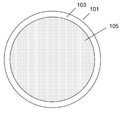
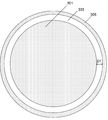
도 1a 및 도 1b는 본 명세서에 제공된 장치 내에서 프로세싱될 수 있는 2개의 이종 웨이퍼 기판들의 개략적인 평면도들을 도시한다.
도 2a는 본 명세서에 제공된 제 1 구성에 따른 전기도금 장치의 개략적인 단면도이다.
도 2b는 본 명세서에 제공된 제 2 구성에 따른 전기도금 장치의 개략적인 단면도이다.
도 3a는 본 명세서에 제공된 일 실시예에 따른, 세그먼트화된 이온 저항성 이온 투과성 엘리먼트의 평면도를 도시한다.
도 3b는 본 명세서에 제공된 실시예에 따른, 세그먼트화된 이온 저항성 이온 투과성 엘리먼트의 평면도를 도시한다.
도 3c는 도 3b에 예시된 세그먼트화된 이온 저항성 이온 투과성 엘리먼트의 일부분의 단면도이다.
도 3d는 본 명세서에 제공된 장치들 내에서 사용될 수 있는 웨이퍼의 표면에서의 전해액의 측면의 플로우를 제공하기 위한 어셈블리의 도면을 도시한다.
도 3e는 본 명세서에 제공된 장치들 내에서 사용될 수 있는 웨이퍼의 표면에서의 전해액의 측면의 플로우를 제공하기 위한 어셈블리의 또 다른 실시예의 도면을 도시한다.
도 4는 도금 챔버의 애노드액 부분과 캐소드액 부분을 분리하는 맴브레인 및 도금 챔버의 캐소드액 부분으로부터 2차 전극 챔버를 분리하는 맴브레인을 포함하는 어셈블리의 등축도이다.
도 5는 본 명세서에 제공된 실시예에 따른 2차 전극 챔버의 개략적인 단면도를 제공한다.
도 6은 본 명세서에 제공된 실시예에 따른 버블 제거 메커니즘을 예시하는 2차 전극 챔버의 개략적인 단면도를 제공한다.
도 7은 2차 애노드가 있거나 없는 시스템들 내의 방사상 도금 균일도를 예시하는 연산 모델링에 의해 제공된 플롯을 도시한다.
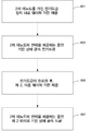
도 8은 본 명세서에 제공된 실시예들 중 일 실시예에 따른 프로세스에 대한 프로세스 흐름도이다.
도 9는 본 발명의 일부 실시예들에 따른, 방위각으로 비대칭으로 배치된 이온 불투과성 부분을 가진 방위각으로 비대칭인 이온 저항성 이온 투과성 엘리먼트의 평면도이다.Figures 1A and 1B show schematic plan views of two different wafer substrates that can be processed in the apparatus provided herein.
2A is a schematic cross-sectional view of an electroplating apparatus according to the first configuration provided herein.
2B is a schematic cross-sectional view of the electroplating apparatus according to the second configuration provided herein.
3a shows a top view of a segmented ion-resistant ion-permeable element, according to one embodiment provided herein.
3B shows a top view of a segmented ion-resistant ion-permeable element, according to an embodiment provided herein.
3C is a cross-sectional view of a portion of the segmented ion-resistant ion-permeable element illustrated in FIG. 3B.
FIG. 3D shows a diagram of an assembly for providing a side flow of electrolyte at a surface of a wafer that can be used in the devices provided herein.
3E shows a view of another embodiment of an assembly for providing a side flow of electrolyte at a surface of a wafer that can be used in the devices provided herein.
4 is an isometric view of an assembly including a membrane separating the anode liquid portion and the cathode liquid portion of the plating chamber and a membrane separating the secondary electrode chamber from the cathode liquid portion of the plating chamber.
Figure 5 provides a schematic cross-sectional view of a secondary electrode chamber in accordance with the embodiment provided herein.
Figure 6 provides a schematic cross-sectional view of a secondary electrode chamber illustrating a bubble removal mechanism in accordance with the embodiment provided herein.
Figure 7 shows plots provided by computational modeling illustrating radial plating uniformity in systems with and without secondary anodes.
8 is a process flow diagram for a process according to an embodiment of the presently disclosed embodiments.
9 is a plan view of an azimuthally asymmetric ion-resistant ion-permeable element having an ion-impermeable portion disposed azimuthally asymmetrically, in accordance with some embodiments of the present invention.
방사상 균일도, 방위각 균일도, 또는 양자와 같은, 전기도금된 층의 균일도를 제어하면서 기판 상에 금속을 전기도금하기 위한 방법들 및 장치가 제공된다. 방법들은 표면 상의 리세스된 피처들의 분포 또는 상이한 패턴들을 가진 반도체 웨이퍼들과 같은, 이종 기판들 상에 금속을 연속적으로 전기도금하는데 특히 유용하다. 방법들은 원격으로 배치된 2차 전극을 사용하여 기판에서 도금 전류 (이온 전류) 를 제어한다.Methods and apparatus are provided for electroplating metal on a substrate while controlling the uniformity of the electroplated layer, such as radial uniformity, azimuthal uniformity, or both. The methods are particularly useful for continuously electroplating metal on heterogeneous substrates, such as semiconductor wafers with a distribution of recessed features on the surface or different patterns. The methods use a remotely located secondary electrode to control the plating current (ion current) in the substrate.
일반적으로 기판이 반도체 웨이퍼인 실시예들이 기술되지만; 본 발명은 이로 제한되지 않는다. 제공된 장치 및 방법들은 TSV 및 WLP 애플리케이션들에서 금속들을 전기도금하는데 유용하지만, 또한 다마신 피처들 내의 구리의 증착을 포함하는 다양한 다른 전기도금 프로세스들에서 사용될 수 있다. 제공된 방법들을 사용하여 전기도금될 수 있는 금속들의 예들은, 제한 없이, 구리, 은, 주석, 인듐, 크롬, 주석-납 합성물, 주석-은 합성물, 니켈, 코발트, 니켈 코발트 합금, 텅스텐을 가진 니켈 및/또는 코발트 합금들, 주석-구리 합성물, 주석-은-구리 합성물, 금, 팔라듐, 및 이들 금속들 및 합성물들을 포함하는 다양한 합금들을 포함한다.Although embodiments in which the substrate is a semiconductor wafer are generally described; The present invention is not limited thereto. The devices and methods provided are useful for electroplating metals in TSV and WLP applications, but can also be used in a variety of other electroplating processes including deposition of copper in damascene features. Examples of metals that can be electroplated using the methods provided include, but are not limited to, copper, silver, tin, indium, chromium, tin-lead compounds, tin-silver compounds, nickel, cobalt, nickel cobalt alloys, nickel with tungsten And / or various alloys including cobalt alloys, tin-copper composites, tin-silver-copper composites, gold, palladium, and metals and composites thereof.
통상적인 전기도금 프로세스에서, 반도체 웨이퍼 기판의 표면 상에 하나 이상의 리세스된 피처들을 가질 수도 있는 반도체 웨이퍼 기판은 웨이퍼 홀더 내로 배치되고, 반도체 웨이퍼 기판의 도금 가능한 (작업) 표면은 전기도금 욕 내에 포함된 전해액 내로 침지된다. 웨이퍼 기판은 웨이퍼 기판이 전기도금 동안 캐소드의 역할을 하도록 네거티브로 바이어스된다. 전해액 내에 포함되는 (상기에 나열된 금속들의 이온들과 같은) 도금 가능한 금속의 이온들은 전기도금 동안 네거티브로 바이어스된 기판의 표면에서 감소되고, 이로써 도금된 금속의 층을 형성한다. 통상적으로 전기도금 동안 회전되는 웨이퍼는 다양한 이유들로 불균일할 수도 있는 전기장 (전해액의 이온 전류장) 을 겪는다. 이것은 금속의 불균일한 증착을 야기할 수도 있다. 불균일도의 타입들 중 일 타입은 동일한 방위각 (각) 위치에서 웨이퍼 상의 상이한 방사상 위치들에서의 도금의 상이한 두께들을 나타내는 중심-대-에지 (또는 방사상) 불균일도이다. 방사상 불균일도는 웨이퍼 기판 상의 전기 콘택트들 부근에 증착되는 보다 많은 양의 금속에 기인하여, 터미널 효과로부터 발생할 수도 있다. 전기 콘택트들이 웨이퍼의 주변에서 이루어지기 때문에, 웨이퍼의 에지 둘레에서, "터미널 효과"로서 지칭되는, 금속 씨드 층 내의 전류의 플로우에 대한 저항은, 기판의 중심과 비교할 때 웨이퍼 기판의 에지에서 보다 두꺼운 도금을 나타낸다. 터미널 효과에 기인하여 방사상 불균일도를 감소시킬 수 있는 방법들 중 일 방법은 기판에 아주 근접하여 배치된 이온 저항성 이온 투과성 엘리먼트의 사용이고, 엘리먼트는 엘리먼트의 중심으로부터 특정한 방사상 위치에서 종료하는 이온 투과성 (예를 들어, 다공성) 구역 및 선택된 방사상 위치를 넘어 이온 불투과성 구역을 가진다. 이것은 엘리먼트가 선택된 반경을 넘어 투과성이 아니기 때문에 선택된 반경을 넘어 엘리먼트를 통해 이온 전류의 플로우를 억제하는 것을 발생시킨다. 단독으로 또는 조합하여 사용되는 또 다른 방법은 웨이퍼 기판의 에지로부터 보다 중심 위치로 도금 전류를 차단하거나 방향 전환하는 환형 실드의 배치이다.In a typical electroplating process, a semiconductor wafer substrate, which may have one or more recessed features on the surface of the semiconductor wafer substrate, is placed into the wafer holder and the platable (working) surface of the semiconductor wafer substrate is contained within the electroplating bath And then immersed in the electrolytic solution. The wafer substrate is negatively biased such that the wafer substrate serves as a cathode during electroplating. Ions of the platable metal (such as the ions of the metals listed above) contained in the electrolyte are reduced at the surface of the negatively biased substrate during electroplating, thereby forming a layer of plated metal. The wafer, which is typically rotated during electroplating, suffers from an electric field (ion current field of the electrolyte) which may be uneven for various reasons. This may cause non-uniform deposition of the metal. One type of type of non-uniformity is center-to-edge (or radial) non-uniformity that represents different thicknesses of plating at different radial positions on the wafer at the same azimuth (angular) position. Radial non-uniformity may also result from terminal effects due to the greater amount of metal deposited near electrical contacts on the wafer substrate. Because electrical contacts are made at the periphery of the wafer, the resistance to the flow of current in the metal seed layer, referred to as "terminal effect ", around the edge of the wafer is greater than at the edge of the wafer substrate Plated. One method of reducing radial inhomogeneities due to terminal effects is the use of an ion-resistant ion-permeable element disposed in close proximity to the substrate, wherein the element has an ion permeability (" E. G., Porous) zone and an ion-impermeable zone beyond the selected radial position. This results in suppressing the flow of ion current through the element beyond the selected radius because the element is not transparent beyond the selected radius. Another method used alone or in combination is the placement of an annular shield that blocks or redirects the plating current from the edge of the wafer substrate to a more central position.
그러나, 많은 경우들에서, 이종 기판들, 예를 들어, 기판들의 표면 상에 리세스된 피처들의 상이한 분포를 갖는 기판들은 기판들의 표면에서 도금 전류의 상이한 분포를 겪을 것이고 불균일도를 감소시키도록 상이한 실드들을 필요로 할 수도 있다. 리세스된 피처들의 상이한 분포를 가진 2개의 반도체 웨이퍼들은 도 1a 및 도 1b에 개략적으로 예시된다. 도 1a에 도시된 웨이퍼 (101) 는 도금 가능하지 않고 포토레지스트로 커버되는 외측 구역 (103), 및 도금 가능한 리세스된 피처들을 포함하는 중심 구역 (105) 을 가진다. 이종 웨이퍼 (107) 는 도 1b에 도시된다. 이 웨이퍼는 실질적으로 모든 웨이퍼 위에서 도금 가능한 피처들을 가진다. 이러한 이종 웨이퍼들이 일 전기도금 툴을 사용하여 연속적으로 프로세싱될 때, 방사상 불균일도 문제에 부닥친다. 툴이 웨이퍼 (107) 의 균일한 도금을 위해 최적화된 개구를 가진 환형 실드를 사용한다면, 웨이퍼 (101) 상의 전기도금을 위한 동일한 툴의 사용은 도금 불가능한 외측 구역 (103) 의 존재에 기인하여 구역 (105) 에 모이는 전류 때문에, 구역 (105) 의 주변 둘레에서 에지-두꺼운 도금을 발생시킬 것이다. 이 효과를 보상하도록, 개구의 보다 작은 직경을 가진 환형 실드는 웨이퍼 (101) 를 프로세싱할 때 사용되어야 한다. 따라서, 웨이퍼들 (101 및 107) 이 연속적으로 프로세싱될 때, 중심 개구의 상이한 직경들을 가진 실드들은 종래의 방법으로 최적의 불균일도를 달성하도록 사용될 필요가 있다. 예를 들어, 300 ㎜ 웨이퍼가 사용될 때, 11.45 인치 (290.8 ㎜) 의 내측 개구의 직경을 가진 실드는 "완전한 대면 노출된" 웨이퍼 (107) 를 프로세싱하기 위해 사용될 수도 있고, 반면에 10.80 인치 (274.3 mm) 의 내측 개구의 직경을 가진 실드는 에지에서 패터닝되지 않은 포토레지스트의 구역을 가진 웨이퍼 (101) 를 프로세싱하는데 잘 맞을 것이다. 그러나, 실딩 (shielding) 사이즈 및 실딩 엘리먼트의 이 변화는 툴 하드웨어의 변화가 상당한 조작자 개입 및 연관된 비생산적인 툴 다운시간을 필요로 하기 때문에 바람직하지 않고 실현 불가능하다. 그러므로 실드 변화들 또는 다른 하드웨어 수정들과 같은 수동 개입의 필요 없이 이종 웨이퍼들을 프로세싱할 수 있을 장치가 필요하다. 보다 일반적으로, 본 명세서에 제공된 장치들 및 방법들을 사용하여 프로세싱될 수 있는 이종 웨이퍼들은 상이한 직경들, 씨드 층들의 상이한 저항률들, 및 리세스된 피처들의 상이한 분포들을 가진 웨이퍼들을 포함한다. 일부 실시예들에서, 웨이퍼들 사이의 차이들은 방사상 균일도에만 영향을 미친다. 다른 실시예들에서, 웨이퍼들 사이의 패턴 레이아웃의 차이들은 방위각 균일도에만 또는 방위각 균일도 및 방사상 균일도에 영향을 미친다.In many cases, however, the substrates with different distributions of the recessed features on the surfaces of the dissimilar substrates, for example, the substrates, will experience different distributions of plating current at the surfaces of the substrates, Shields may be needed. Two semiconductor wafers with different distributions of the recessed features are schematically illustrated in Figs. 1A and 1B. The
도금 전류를 웨이퍼 기판으로 공여하고 그리고/또는 도금 전류를 웨이퍼 기판으로부터 방향 전환하도록 구성되는 적절하게 배치된 제 2 전극은 본 명세서에 제공된 실시예들에서 도금 균일도를 조절하도록 사용된다. 전기도금 시스템의 다른 컴포넌트들 (components) 에 관하여 전극의 위치는 제작 복잡성 및 비용의 최소화, 신뢰도의 개선, 및 어셈블리 및 유지 보수의 용이성을 포함하는 복수의 이유들에 있어서 매우 중요하다. 전기도금 장치의 2개의 메인 구성들이 도시된다. 구성들은 제 2 전극이 맴브레인에 의해 분리되는 애노드액 격실과 캐소드액 격실을 포함하는 전기도금 시스템 내에 어떻게 통합될 수 있는지를 예시한다. 구성들은 2차 전극이 기판의 부근에 배치된 CIRP (channeled ionically resistive plate) 와 같은 이온 저항성 이온 투과성 엘리먼트와 어떻게 통합될 수 있는지를 더 도시한다. 구성들 양자는 Lam Research Corporation으로부터 입수 가능한 Sabre 3DTM 시스템에서 구현될 수 있다.A suitably disposed second electrode configured to donate plating current to the wafer substrate and / or to divert the plating current from the wafer substrate is used to adjust the plating uniformity in the embodiments provided herein. The location of the electrodes with respect to other components of the electroplating system is of great importance for a number of reasons, including fabrication complexity and cost minimization, reliability improvement, and ease of assembly and maintenance. Two main arrangements of the electroplating apparatus are shown. The configurations illustrate how the second electrode can be integrated in an electroplating system comprising an anode liquid compartment and a cathode liquid compartment separated by a membrane. The configurations further illustrate how the secondary electrode can be integrated with an ion-resistant ion-permeable element such as a channeled ionically resistive plate (CIRP) disposed in the vicinity of the substrate. Both configurations can be implemented in a Saber 3D TM system available from Lam Research Corporation.
도금 용기의 애노드액 부분 및 캐소드액 부분The anode liquid portion of the plating vessel and the cathode liquid portion
본 명세서에 제공된 장치의 구성들 양자에서, 전기도금 장치는 전해액을 홀딩하도록 구성된 도금 챔버를 포함하고, 도금 챔버는 이온-투과성 맴브레인에 의해 애노드액 격실 및 캐소드액 격실로 분리된다. 1차 애노드는 애노드액 부분 내에 하우징되지만, 기판은 맴브레인을 넘어 캐소드액 부분 내의 전해액 내로 침지된다. 애노드액의 조성물 (애노드액 격실 내의 전해액) 및 캐소드액의 조성물 (캐소드액 격실 내의 전해액) 은 동일하거나 상이할 수 있다.In both of the arrangements of the apparatus provided herein, the electroplating apparatus includes a plating chamber configured to hold an electrolyte solution, and the plating chamber is separated into an anode liquid compartment and a cathode liquid compartment by an ion-permeable membrane. The primary anode is housed in the anode liquid portion, but the substrate is immersed in the electrolyte solution in the cathode liquid portion beyond the membrane. The composition of the anode liquid (electrolytic solution in the anode liquid compartment) and the composition of the cathode liquid (electrolytic solution in the cathode liquid compartment) may be the same or different.
맴브레인은 1차 애노드에서 생성된 입자들이 웨이퍼의 부근에 들어가고 웨이퍼를 오염시키는 것을 방지하는 동안, 도금 셀의 애노드액 구역 및 캐소드액 구역 사이의 이온 연통을 허용한다. 일부 실시예들에서, 맴브레인은 이온 이동 (전기장의 인가에 응답하는 운동) 을 통해 전해액 내에 포함된 하나 이상의 대전된 종의 상대적으로 자유로운 이동을 허용하는 동안, 압력 구배들의 영향 하에서 용해된 컴포넌트들 및 용매의 물리적인 이동을 실질적으로 방지할 수 있는 나노다공성 맴브레인 (이로 제한되지 않지만 역삼투 맴브레인, 카티온 (cationic) 맴브레인 또는 아니온 (anionic) 맴브레인을 포함) 이다. 적합한 애노드의 맴브레인들의 상세한 기술들은 모든 목적들을 위해 참조로서 본 명세서에 인용되는 Reid 등에 허여된 미국 특허들 6,126,798 호 및 6,569,299 호에 제공된다. 카티온 교환 맴브레인들과 같은 이온 교환 맴브레인들은 이들 애플리케이션들에 특히 적합하다. 이들 맴브레인들은 통상적으로 설폰기들을 포함하는 퍼플루오리네이트 코-폴리머들 (예를 들어 나피온), 설포네이트 폴리이미드들과 같은 이오노머 (ionomeric) 재료들, 및 카티온 (cation) 교환에 적합한 것으로 당업자에게 알려진 다른 재료들로 이루어진다. 적합한 나피온 맴브레인들의 선택된 예들은 Dupont de Nemours Co.로부터 입수 가능한 N324 맴브레인 및 N424 맴브레인을 포함한다. 캐소드액과 애노드액을 분리하는 맴브레인은 상이한 카티온들에 대해 상이한 선택도를 가질 수도 있다. 예를 들어, 맴브레인은 금속 이온들 (예를 들어 구리 이온들) 의 통과 레이트보다 보다 빠른 레이트로 양성자들의 통과를 허용할 수도 있다.The membrane permits ionic communication between the anode liquid zone and the cathode liquid zone of the plating cell while preventing particles generated in the primary anode from entering the vicinity of the wafer and contaminating the wafer. In some embodiments, the membrane may be configured to allow dissolved components and / or components to flow under the influence of pressure gradients, while allowing the relatively free movement of the one or more charged species contained in the electrolyte through ion movement (movement in response to application of the electric field) (Including, but not limited to, reverse osmosis membrane, cationic membrane, or anionic membrane) capable of substantially preventing physical migration of the solvent. Detailed descriptions of suitable anode membranes are provided in U.S. Patent Nos. 6,126,798 and 6,569,299 to Reid et al., Which are hereby incorporated by reference for all purposes. Ion exchange membranes such as cation exchange membranes are particularly suitable for these applications. These membranes are typically suitable for ionomeric materials such as perfluorinated co-polymers (e.g., Nafion), sulfonate polyimides including sulfonic groups, and cation exchange And other materials known to those skilled in the art. Selected examples of suitable Nafion membranes include N324 membranes and N424 membranes available from Dupont de Nemours Co. The membrane separating the catholyte and the anolyte may have different selectivities for different cations. For example, the membrane may allow the passage of protons at a faster rate than the pass rate of metal ions (e.g., copper ions).
맴브레인-분리된 캐소드액 격실 및 애노드액 격실을 가진 전기도금 장치는 캐소드액과 애노드액의 분리를 달성하고 캐소드액 격실 및 애노드액 격실로 하여금 별개의 조성물들을 갖게 한다. 예를 들어, 유기 첨가제들은 캐소드액 내에 포함될 수 있지만, 애노드액은 본질적으로 첨가제 없이 남아 있을 수 있다. 또한, 애노드액 및 캐소드액은 예를 들어, 맴브레인의 이온 선택도에 기인하여, 상이한 농도들의 금속 염 및 산을 가질 수도 있다. 맴브레인을 가진 전기도금 장치는 모든 목적들을 위해 참조로서 본 명세서에 인용되는 Mayer 등에 허여된 미국 특허 6,527,920 호에 상세히 기술된다.An electroplating apparatus having a membrane-separated cathode liquid compartment and an anode liquid compartment achieves separation of the cathode liquid and the anode liquid and allows the cathode liquid compartment and the anode liquid compartment to have separate compositions. For example, organic additives may be included in the catholyte, but the anolyte may remain essentially free of additives. In addition, the anolyte and the catholyte may have different concentrations of the metal salt and acid, for example due to the ion selectivity of the membrane. Electroplating apparatuses with membranes are described in detail in US Patent 6,527,920 to Mayer et al., Which is hereby incorporated by reference for all purposes.
본 명세서에 제공된 전기도금 장치의 구성들 양자에서, 2차 전극은 2차 전극에 의해 공여되고 그리고/또는 방향 전환된 도금 전류가 도금 챔버의 애노드액 부분 및 캐소드액 부분을 분리하는 맴브레인을 통과하지 않도록 배치된다.In both of the configurations of the electroplating apparatus provided herein, the secondary electrode is donated by the secondary electrode and / or a plating current that is redirected does not pass through the membrane separating the anode liquid portion and the cathode liquid portion of the plating chamber .
이온 저항성 이온 투과성 엘리먼트Ion-resistant ion-permeable element
본 명세서에 제공된 장치의 구성들 양자에서, 장치는 도금 챔버의 캐소드액 격실 내의 기판의 근처에 배치된 이온 저항성, 이온 투과성 엘리먼트를 포함한다. 이것은 엘리먼트를 통한 전해액의 이송 및 자유 플로우를 허용하지만, 도금 시스템 내로 상당한 이온 저항을 도입하고, 그리고 중심-대-에지 (방사상) 균일도를 개선할 수도 있다. 일부 실시예들에서, 이온 저항성 이온 투과성 엘리먼트는 기판의 작업 면에 실질적으로 수직인 방향으로 엘리먼트를 나가는 전해액 플로우 (충돌 플로우) 의 소스의 역할을 더 하고, 그리고 주로 플로우-성형 엘리먼트로서 기능한다. 일부 실시예들에서 엘리먼트는 웨이퍼 기판의 도금 가능한 표면에 수직인 채널들 또는 홀들을 포함한다. 일부 실시예들에서 엘리먼트는 웨이퍼 기판의 도금 가능한 표면에 대해 90 도와 상이한 각에 있는 채널들 또는 홀들을 포함한다. 통상적인 이온 저항성 이온 투과성 엘리먼트는 도금 셀 시스템의 전체 전압 강하의 80 % 이상을 차지한다. 대조적으로, 이온 저항성 이온 투과성 엘리먼트는 매우 낮은 유체 플로우 저항을 갖고 셀 및 보조적인 지지 배관 네트워크 시스템의 압력 강하에 매우 적게 기여한다. 이것은 엘리먼트 (예를 들어, 직경에 있어서 약 12 인치 또는 700 ㎠) 의 큰 피상적인 표면적 및 적당한 다공률 및 구멍 사이즈들 때문이다 (예를 들어 엘리먼트는 약 0.4 내지 0.8 ㎜의 직경을 가질 수도 있는 적절한 수의 드릴링된 채널들 (또한 구멍들 또는 홀들로서 지칭됨) 에 의해 생성된 약 1 내지 5 %의 다공률을 가질 수도 있다). 예를 들어, 4.5 %의 다공률 및 0.5 인치의 두께를 가진 다공성 플레이트 (예를 들어, 0.026" 직경을 가진 9600개의 드릴링된 홀들을 포함하는 플레이트) 를 통해 20 리터/분으로 흘리기 위해 계산된 압력 강하는 1 인치 미만의 수압 (대략 0.036 psi와 동일) 이다. 적합한 이온 저항성 이온 투과성 엘리먼트들은 예를 들어, 전체가 참조로서 본 명세서에 인용되는 2012년 11월 13일에 허여된 미국 특허 제 8,308,931 호에 상세히 기술된다. 일반적으로 이온 저항성 이온 투과성 엘리먼트는 엘리먼트의 바디 내에서 상호 연결된 채널들을 형성하는 구멍들을 포함할 수도 있지만 많은 실시예들에서 엘리먼트의 바디 내에서 상호 연결되지 않은 채널들을 가진 엘리먼트를 사용하는 것 (예를 들어, 상호 연결되지 않은 드릴링된 홀들을 가진 플레이트를 사용하는 것) 이 보다 바람직하다. 후자의 실시예는 CIRP로서 지칭된다. CIRP의 2개의 특징들은 특히 중요하다: 기판에 대해 아주 근접하게 CIRP 배치, 및 CIRP 내의 쓰루홀들이 서로로부터 공간적으로 그리고 이온 절연되고 CIRP의 바디 내에서 상호 연결된 채널들을 형성하지 않는다는 사실. 이러한 쓰루홀들은 쓰루홀들이 1차원으로, 종종, 반드시 그러한 것은 아니지만, 기판의 도금된 표면에 수직으로 연장하기 때문에 1-D 쓰루홀들로서 지칭될 것이다 (일부 실시예에서 1-D 홀들은 CIRP 전면에 대체로 평행인 웨이퍼에 대해 비스듬히 있음). 채널들이 3차원으로 연장하고 상호 연결된 구멍 구조체들을 형성하는 경우에, 이들 쓰루홀들은 3-D 다공성 네트워크들로부터 구별된다. CIRP의 예는 약 6,000 내지 12,000개의 1-D 쓰루홀들을 가진, 폴리에틸렌, 폴리프로필렌, PVDF (polyvinylidene difluoride), 폴리테트라플루오로에틸렌, 폴리설폰, PVC (polyvinyl chloride), 폴리카보네이트, 등과 같은 이온 저항성 재료로 이루어진 디스크이다. 많은 실시예들에서, 디스크는 (예를 들어, 300 ㎜ 웨이퍼가 사용될 때 약 300 ㎜의 직경을 가진) 웨이퍼와 실질적으로 동일한 공간에 걸치고 웨이퍼와 아주 근접하여, 예를 들어, 단지 웨이퍼-대면-하향 전기도금 장치 내에서 웨이퍼 아래에 존재한다. 바람직하게, 웨이퍼의 도금된 표면은 약 10 ㎜ 내에, 더 바람직하게 가장 가까운 CIRP 표면의 약 5 ㎜ 내에 존재한다. 본 명세서에 기술될 장치의 제 2 구성에서 CIRP는 적어도 3개의 세그먼트들: 1차 애노드로부터 도금 전류를 통과시키도록 구성된 내측 세그먼트, 2차 전극으로부터 전류를 통과시키도록 구성된 외측 세그먼트, 및 내측 세그먼트와 외측 세그먼트를 서로 전기적으로 절연하고 도금 전류들이 CIRP 또는 CIRP의 바디 내에 들어가기 전에 1차 애노드 및 2차 전극으로부터의 도금 전류들로 하여금 혼합되게 하지 않는 내측 세그먼트와 외측 세그먼트 사이의 데드 존 (dead zone) 을 포함한다.In both of the arrangements of the apparatus provided herein, the apparatus comprises an ion-resistant, ion-permeable element disposed in the vicinity of the substrate in the cathode liquid compartment of the plating chamber. This allows transfer and free flow of electrolyte through the element, but may introduce significant ionic resistance into the plating system and improve center-to-edge (radial) uniformity. In some embodiments, the ion-resistant ion-permeable element acts as a source of electrolyte flow (impingement flow) exiting the element in a direction substantially perpendicular to the working surface of the substrate, and functions primarily as a flow-shaping element. In some embodiments, the element comprises channels or holes perpendicular to the platable surface of the wafer substrate. In some embodiments, the element includes angled channels or holes that are 90 degrees different than the platable surface of the wafer substrate. Typical ion-resistant ion-permeable elements account for more than 80% of the total voltage drop of the plating cell system. In contrast, the ion-resistant ion-permeable element has a very low fluid flow resistance and contributes very little to the pressure drop of the cell and ancillary support piping network systems. This is due to the large superficial surface area and appropriate porosity and pore sizes of the elements (e.g., about 12 inches or 700 cm2 in diameter) (e.g., the elements may have a diameter of about 0.4 to 0.8 mm And may have a porosity of about 1 to 5% produced by a number of drilled channels (also referred to as holes or holes). For example, calculated pressures to flow at 20 liters / minute through porous plates with a porosity of 4.5% and a thickness of 0.5 inches (e.g., plates containing 9600 drilled holes with 0.026 "diameter) The drop is a water pressure of less than one inch (equivalent to approximately 0.036 psi). Suitable ion resistive ion permeable elements are described, for example, in U.S. Patent No. 8,308,931, issued November 13, 2012, In general, the ion-resistant ion-permeable element may include holes that form interconnected channels in the body of the element, but in many embodiments use an element having channels that are not interconnected in the body of the element (E. G., Using plates with drilled holes that are not interconnected) Two features of the CIRP are particularly important: the CIRP placement in close proximity to the substrate, and the through-holes in the CIRP are spatially and ionically isolated from each other and within the body of the CIRP These through-holes will be referred to as 1-D through-holes because the through-holes extend in one dimension, often, but not necessarily, perpendicular to the plated surface of the substrate In the example, 1-D holes are oblique to a wafer that is generally parallel to the front of the CIRP.) In the case where the channels extend in three dimensions and form interconnected interconnect structures, these through holes are distinguished from 3-D porous networks . Examples of CIRPs include polyethylene, polypropylene, polyvinylidene difluoride (PVDF), polyvinylidene difluoride (PVDF) (For example, a 300 mm wafer when a 300 mm wafer is used), a disk made of an ion resistant material such as polytetrafluoroethylene, polysulfone, polyvinyl chloride, polycarbonate, etc. In many embodiments, Mm) and is in close proximity to the wafer, for example, just below the wafer in a wafer-facing-down electroplating apparatus. Preferably, the plated surface of the wafer is within about 10 mm, more preferably within about 5 mm of the nearest CIRP surface. In a second configuration of the device described herein, the CIRP comprises at least three segments: an inner segment configured to pass a plating current from the primary anode, an outer segment configured to pass current from the secondary electrode, A dead zone between the inner and outer segments that electrically isolates the outer segments from one another and does not allow the plating currents from the primary anode and the secondary electrode to mix before the plating currents enter the body of the CIRP or CIRP, .
기판과 가까운, 저항성이지만 이온 투과성 엘리먼트의 존재는 터미널 효과의 영향을 실질적으로 감소시키고 터미널 효과를 보상하고 방사상 도금 균일도를 개선한다. 또한 동시에 플로우 확산 매니폴드 플레이트로서 역할을 함으로써 웨이퍼 표면으로 상향으로 지향된 전해액의 실질적으로 공간적으로-균일한 충돌 플로우를 갖는 능력을 제공한다. 중요하게, 동일한 엘리먼트가 웨이퍼로부터 멀리 배치된다면, 플로우 개선들 및 이온 전류의 균일도는 상당히 덜 단언되거나 (pronounce) 존재하지 않게 된다. 추가로, 1-D 쓰루홀들이 CIRP 내에서 유체 운동 또는 이온 전류의 측면 이동을 허용하지 않기 때문에, 중심-대-에지 전류 및 플로우 이동들은 CIRP 내에서 차단되고, 방사상 도금 균일도의 추가의 개선을 야기한다.The presence of a resistive but ion-permeable element close to the substrate substantially reduces the effect of the terminal effect, compensates for terminal effects and improves radial plating uniformity. And also provides the ability to have a substantially spatially-homogeneous impingement flow of the electrolyte upward directed to the wafer surface by acting as a flow diffusion manifold plate at the same time. Significantly, if the same element is placed away from the wafer, the flow improvements and the uniformity of the ion current become much less pronounced or absent. In addition, since 1-D through holes do not allow fluid movement or lateral movement of ion currents within the CIRP, the center-to-edge current and flow movements are blocked within the CIRP, further improving radial plating uniformity It causes.
CIRP 구조체의 또 다른 중요한 특징은 쓰루홀들의 직경 또는 주요 치수 및 CIRP와 기판 사이의 거리에 대한 쓰루홀의 관계이다. 바람직하게 쓰루홀 (또는 다수의 쓰루홀들) 각각의 직경은 도금된 기판 표면으로부터 CIRP의 가장 가까운 표면으로의 거리보다 짧아야 한다. 따라서, 쓰루홀들의 직경 또는 주요 치수는 CIRP가 도금된 웨이퍼 표면의 약 5 ㎜ 내에 배치될 때 5 ㎜를 초과해서는 안된다.Another important feature of the CIRP structure is the diameter or major dimension of the through holes and the relationship of the through holes to the distance between the CIRP and the substrate. Preferably, the diameter of each of the through holes (or multiple through holes) should be less than the distance from the plated substrate surface to the nearest surface of the CIRP. Thus, the diameter or major dimension of the through holes should not exceed 5 mm when the CIRP is placed within about 5 mm of the plated wafer surface.
일부 실시예들에서 이온 저항성 이온 투과성 엘리먼트 (예를 들어, CIRP) 는 기판의 도금된 표면과 평행한 상단 표면을 가진다. 다른 실시예들에서, 이온 저항성 이온 투과성 엘리먼트의 상단 표면은 오목하거나 볼록하다.In some embodiments, the ion-resistant ion-permeable element (e.g., CIRP) has a top surface parallel to the plated surface of the substrate. In other embodiments, the upper surface of the ion-resistant ion-permeable element is concave or convex.
장치는 또한 도금 유체가 이온 저항성 이온 투과성 엘리먼트의 표면과 실질적으로 평행한 방향으로 주입될 때에도, 이온 저항성 엘리먼트를 통한 후방으로의 도금 유체의 플로우가 실질적으로 방지되도록 구성된다. 물과 같은 비압축성 유체들의 운동이 관성력과 점성력의 밸런스 및 스케일링의 다양한 레벨들을 수반한다는 것을 유념하는 것은 중요하다. 유체 동적인 Navier-Stokes 방정식들 및 유체 플로우 거동이 중요한 관성 항들을 가진 텐서 (tensor) (벡터) 방정식들에 의해 지배된다는 사실을 고려하면, 도금 액체가 아래의 매니폴드로부터 이온 저항성 이온 투과성 엘리먼트를 통해 그리고 매니폴드를 통해 "상향으로" 흐르게 하는 것이 손쉬울 수도 있지만 (저압이 상당한 양의 플로우를 얻도록 요구되기 때문에), 대조적으로, 표면에 평행하게 흐르는 유체는 동일한 정압에서 다공성 재료를 통과하는 것에 대해 매우 적은 경향 및 "고 저항"을 가질 수도 있다는 것이 이해될 수 있다. 표면과 수직인 이동으로, 표면과 평행한 신속한 이동으로부터 직각으로의 유체의 이동의 방향을 변화시키는 것은, 유체의 에너지의 점성 소실 및 유체의 감속을 수반하고, 그러므로 매우 적합하지 않을 수 있다. 배경에 대해, 이 발명의 다른 실시예들에서, 이온 저항성 이온 투과성 엘리먼트는 웨이퍼 및 CIRP 표면과 평행한 축과 평행한 방향으로 상대적으로 고속으로 유체를 이동시키기 위한 주변의 보조적인 수단 (예를 들어 유체 주입기) 을 갖고, 상기 CIRP 엘리먼트는 유체가 엘리먼트를 통해 이동하는 것 및 엘리먼트 내로 통과함으로써 엘리먼트들의 채널들의 출구측으로, 엘리먼트 아래 및 맴브레인 위의 매니폴드를 통해, 그리고 이어서 후방으로 셀의 크로스-플로우 배기측 근방의 엘리먼트를 통해 전이하는 것을 실질적으로 방지한다. 즉, 이온 저항성 이온 투과성 엘리먼트의 구멍 사이즈, 다공률 및 평행한 플로우 속도와 결합된 이온 저항성 이온 투과성 엘리먼트의 존재는 평행한 플로우의 이러한 우회 (circumvention) 가 발생하는 것을 방지할 수 있다. 임의의 특정한 모델 또는 이론에 매이지 않고, 고속 유체는 이온 저항성 엘리먼트와 평행한 운동의 방향으로 상당한 양의 관성을 갖고, 엘리먼트의 구멍들에 들어가도록 직각으로 턴하고 감속될 필요가 있을 것이고, 이와 같이, 이온 저항성 엘리먼트는 유체가 방향을 바꾸고 이온 저항성 엘리먼트를 통과하는 것을 방지하는 매우 양호한 배리어로서 주로 역할을 한다고 여겨진다. 본 명세서에 제공된 전기도금 장치의 2개의 구성들은 이온 저항성 이온 투과성 엘리먼트에 대한 2차 전극의 위치가 다르다. 본 명세서에 제공된 제 1 구성에 따르면, 제 2 전극은 이온 저항성 이온 투과성 엘리먼트 (예를 들어, CIRP) 를 통해 그리고 애노드액 격실과 캐소드액 격실을 분리하는 맴브레인을 통해 공여된 전류를 통과시키지 않고 기판으로 도금 전류를 공여하도록 배치되는 방위각으로 대칭인 애노드 (예를 들어, 링) 이다. 이 구성은 주로 방사상 균일도를 제어하도록 사용되지만, 예를 들어, 부가적인 방위각으로 비대칭이거나 세그먼트화된 3차 전극을 사용하여, 방위각 균일도 제어의 능력을 부가적으로 가질 수 있다.The device is also configured to substantially prevent the flow of plating fluid backward through the ion-resistant element, even when the plating fluid is injected in a direction substantially parallel to the surface of the ion-resistant ion-permeable element. It is important to note that the motion of incompressible fluids such as water involves various levels of balance and scaling of inertial and viscous forces. Taking into account the fact that fluid dynamic Navier-Stokes equations and fluid flow behavior are dominated by tensor (vector) equations with important inertial terms, it is clear that the plating liquid will flow from the underlying manifold to the ion- Flow through the manifold may be handy (since the low pressure is required to obtain a significant amount of flow), but in contrast, the fluid flowing parallel to the surface will pass through the porous material at the same static pressure It can be understood that there may be a very low tendency and "high resistance" Changing the direction of fluid movement from rapid to parallel perpendicular movement to the surface at right angles involves viscous dissipation of the energy of the fluid and slowing of the fluid and may therefore not be very suitable. In contrast to the background, in other embodiments of the present invention, the ion-resistant ion-permeable element is surrounded by ancillary means for moving the fluid at a relatively high velocity in a direction parallel to the axis parallel to the wafer and the CIRP surface Fluid injector), the CIRP element having fluid flow through the element and through the element to the outlet side of the channels of the elements, through the manifold below the element and above the membrane, and then back to the cross- Thereby substantially preventing transition through the element in the vicinity of the exhaust side. That is, the presence of the ion-resistant ion-permeable element combined with the pore size, porosity and parallel flow rate of the ion-resistant ion-permeable element can prevent this circumvention of the parallel flow from occurring. Without being bound to any particular model or theory, the high velocity fluid will have a significant amount of inertia in the direction of motion parallel to the ion resistive element, and will need to be turned and decelerated at right angles to enter the apertures of the element, , It is believed that the ion-resistant element plays a major role as a very good barrier to prevent the fluid from changing direction and passing through the ion-resistant element. The two configurations of the electroplating apparatus provided herein differ in the position of the secondary electrode relative to the ion-resistant ion-permeable element. According to the first configuration provided herein, the second electrode is electrically connected to the substrate through the ion-resistant ion-permeable element (e.g., CIRP) and through the membrane separating the anode liquid compartment and the cathode liquid compartment, (E. G., A ring) symmetrically disposed at an azimuth angle that is arranged to impart a plating current to the anode. This configuration is mainly used to control radial uniformity, but it may additionally have the ability of azimuthal uniformity control, for example, using an asymmetric or segmented tertiary electrode at additional azimuth angles.
전기도금 장치의 제 1 구성의 예Example of First Configuration of Electroplating Apparatus
애노드액 격실과 캐소드액 격실을 분리하는 맴브레인, 웨이퍼에 아주 근접한 저항성 엘리먼트, 및 2차 애노드 양자를 채용하는 제 1 구성의 도금 시스템의 예시가 도 2a에 도시된다. 이것은 도금 시스템의 일 예이고, 도금 시스템은 첨부된 청구항들의 정신 및 범위 내에서 수정될 수 있다는 것이 이해된다. 예를 들어, 환형 실드는 모든 실시예들에서 나타날 필요가 없고, 나타날 때, 실드는 CIRP 아래, CIRP 위에 배치될 수도 있거나, CIRP와 통합될 수 있다.An example of a plating system of a first configuration employing both a membrane separating the anode liquid compartment and the cathode liquid compartment, a resistive element very close to the wafer, and a secondary anode is shown in FIG. It is understood that this is an example of a plating system, and that the plating system can be modified within the spirit and scope of the appended claims. For example, an annular shield need not be present in all embodiments, and when it appears, the shield may be placed below the CIRP, over the CIRP, or may be integrated with the CIRP.
도 2a를 참조하면, 전기도금 장치 (201) 의 개략적인 단면도가 도시된다. 도금 용기 (203) 는 통상적으로 금속 이온들과 산의 소스를 포함하는 도금 용액을 담고있다. 웨이퍼 (205) 는 도금 용액 내로 침지되고 웨이퍼 (205) 와 함께 크램셸 (207) 의 양방향 회전을 허용하는, 회전 가능한 스핀들 (209) 상에 장착된, "크램셸 (clamshell)" 홀딩 픽스처 (207) 에 의해 홀딩된다. 이 발명을 사용하는데 적합한 양태들을 가진 크램셸-타입 도금 장치의 일반적인 기술은 이전에 참조로서 인용된, Patton 등에 허여된 미국 특허 6,156,167 호, 및 Reid 등에 허여된 미국 특허 6,800,187 호에 상세히 기술된다. (불활성 또는 소모성 애노드일 수도 있는) 1차 애노드 (211) 는 도금 욕 (203) 내의 웨이퍼 아래에 배치되고 맴브레인 (213), 바람직하게 이온 선택적 맴브레인에 의해 웨이퍼 구역으로부터 분리된다. 애노드의 맴브레인 아래의 구역 (215) 은 종종 "애노드 챔버" 또는 "애노드액 격실" 및 "애노드액"으로서 이 챔버 내의 전해액으로서 지칭된다. 맴브레인 (213) 위의 구역 (217) 은 "캐소드액 격실"로서 지칭된다. 이온-선택적 애노드 맴브레인 (213) 은 애노드에서 생성된 입자들이 웨이퍼의 부근에 들어가는 것 및 입자들 및/또는 캐소드액 전해액 내에 존재하는 바람직하지 않은 화학 종을 오염시키는 것을 방지하고, 애노드 (211) 와 콘택트하는 것을 방지하는 동안, 도금 셀의 애노드 구역과 캐소드 구역 사이의 이온 연통을 허용한다.Referring to FIG. 2A, a schematic cross-sectional view of an
도금 용액은 펌프 (미도시) 에 의해 도금 욕 (203) 에 연속적으로 제공된다. 일부 실시예들에서, 도금 용액은 웨이퍼와 아주 근접하여 위치된 CIRP (219) (또는 다른 이온 저항성 이온 투과성 엘리먼트) 및 맴브레인 (213) 을 통해 상향으로 흐른다. 다른 실시예들에서, 맴브레인 (213) 이 도금 유체의 플로우에 일반적으로 불투과성일 때 (예를 들어 카티온 맴브레인과 같은 나노다공성 매체) 와 같이, 도금 유체는 맴브레인 (213) 과 CIRP (219) 사이의 도금 챔버, 예를 들어 챔버 주변에 들어가고, 그리고 CIRP를 통해 흐른다. 이 경우에, 애노드 챔버 내의 도금 유체는 순환될 수도 있고 압력은 CIRP 및 캐소드 챔버로부터 별도로 조절될 수 있다. 이러한 분리된 조절은 예를 들어, 전체가 참조로서 본 명세서에 인용되는, 2013년 12월 10일 허여된 미국 특허 제 8,603,305 호 및 2003년 3월 4일 허여된 미국 특허 제 6,527,920 호에 기술된다.The plating solution is continuously supplied to the
2차 애노드 (223) 를 하우징하는 2차 애노드 챔버 (221) 는 도금 용기 (203) 의 외측 및 웨이퍼 주변에 위치된다. 특정한 실시예들에서, 2차 애노드 챔버 (221) 는 이온-투과성 맴브레인 (225) 에 의해 커버된 복수의 개구들을 가진 벽 (맴브레인 지지 구조체) 에 의해 도금 욕 (203) 으로부터 분리된다. 맴브레인은 도금 셀과 2차 애노드 챔버 사이의 이온 연통을 허용하고, 이로써 도금 전류가 제 2 애노드에 의해 공여되게 한다. 이 맴브레인의 다공률은 맴브레인이 미립자 재료로 하여금 2차 애노드 챔버 (221) 로부터 도금 욕 (203) 으로 넘어가게 하지 않고 웨이퍼 오염이 발생하게 하지 않도록 결정된다. 2차 애노드 챔버와 메인 도금 용기 사이의 유체 및/또는 이온 연통을 허용하기 위한 다른 메커니즘들은 이 발명의 범위 내에 있다. 예들은 불투과성 벽보다는 맴브레인이 제 2 캐소드 챔버 내의 도금 용액과 메인 도금 용기 내의 도금 용액 사이에 대부분의 배리어를 제공하는 설계들을 포함한다. 단단한 프레임워크는 이러한 실시예들에서 맴브레인에 지지를 제공할 수도 있다.The
부가적으로, 환형 실드 (227) 와 같은 하나 이상의 실드들이 챔버 내에 배치될 수 있다. 실드들은 보통 모든 목적들을 위해 전체가 참조로서 본 명세서에 인용되는 Broadbent에 허여된 미국 특허 6,027,631 호에 기술된 것들과 같이, 전류 프로파일을 성형하고 도금의 균일도를 개선하기 위해 사용되는, 링-형상의 유전체 삽입부들이다. 물론 다른 실드 설계들 및 형상들이 당업자들에게 공지된 바와 같이 채용될 수도 있다. Additionally, one or more shields, such as the
일반적으로, 실드들은 웨지들, 바들, 원들, 타원들 및 다른 기하학적 설계들의 형상을 포함하는 임의의 형상을 취할 수도 있다. 링-형상의 삽입부들은 또한 삽입부들의 내경에서 패턴들을 가질 수도 있고, 이는 목표된 방식으로 전류 플럭스를 성형할 실드들의 능력을 개선한다. 실드들의 기능은 도금 셀 내의 실드들의 위치에 따라 상이할 수도 있다. 본 발명의 장치는 스태틱 (static) 실드들, 뿐만 아니라 Mayer 등에 허여된 미국 특허 6,402,923 호에 기술된 것들과 같은, 가변 가능한 필드 성형 엘리먼트들, 또는 Woodruff 등에 허여된 미국 특허 6,497,801 호 및, Mayer 등에 허여된 미국 특허 6,773,571 호에 기술된 바와 같은 세그먼트화된 애노드들 중 임의의 것을 포함할 수 있고, 각각은 전체가 참조로서 본 명세서에 인용된다.In general, the shields may take any shape, including shapes of wedges, bars, circles, ellipses, and other geometric designs. The ring-shaped inserts may also have patterns in the inner diameter of the inserts, which improves the ability of the shields to shape the current flux in the desired manner. The function of the shields may differ depending on the position of the shields in the plating cell. The apparatus of the present invention can be used in conjunction with static shields as well as variable field shaping elements such as those described in US Patent 6,402,923 to Mayer et al. Or US Patent 6,497,801 to Woodruff et al. And may include any of the segmented anodes as described in U.S. Patent 6,773,571, each of which is incorporated herein by reference in its entirety.
2개의 DC 전력 공급부들 (미도시) 은 웨이퍼 (205), 1차 애노드 (211) 로 그리고 2차 애노드 (223) 로 각각 전류 플로우를 제어하도록 사용될 수 있다. 대안적으로, 복수의 독립적으로 제어 가능한 전기 유출부들을 가진 일 전력 공급부는 웨이퍼로 그리고 2차 애노드로 상이한 레벨들의 전류를 제공하도록 사용될 수 있다. 전력 공급부 또는 공급부들은 웨이퍼 (205) 를 네거티브로 바이어스하고 1차 애노드 (211) 및 2차 애노드 (223) 를 포지티브로 바이어스하도록 구성된다. 장치는 전기도금 셀의 엘리먼트들에 제공된 전류 및/또는 전위의 조절을 허용하는 제어기 (229) 를 더 포함한다. 제어기는 도금 셀의 다양한 엘리먼트들에 인가될 필요가 있는 전류 레벨 및 전압 레벨, 뿐만 아니라 이들 레벨들이 변화될 필요가 있는 시간들을 명시하는 프로그램 인스트럭션들을 포함할 수도 있다. 예를 들어, 제어기는 2차 애노드에 전력을 공급하기 위한 프로그램 인스트럭션, 및 선택 가능하게 전기도금 동안 2차 애노드에 공급된 전력을 동적으로 가변하기 위한 프로그램 인스트럭션을 포함할 수도 있다.Two DC power supplies (not shown) may be used to control the current flow to the
화살표들은 예시된 장치 내의 도금 전류를 도시한다. 1차 애노드로부터 비롯된 전류는 상향으로 지향되고, 애노드액 격실과 캐소드액 격실을 분리하는 맴브레인과 CIRP를 통과한다. 2차 애노드로부터 비롯된 전류는 도금 용기의 주변으로부터 중심으로 지향되고 애노드액 격실과 캐소드액 격실을 분리하는 맴브레인과 CIRP를 통과하지 않는다.The arrows show the plating current in the illustrated apparatus. The current from the primary anode is directed upward and passes through the membrane and the CIRP separating the anode liquid compartment and the cathode liquid compartment. Current from the secondary anode is directed from the periphery of the plating vessel to the center and does not pass through the membrane and the CIRP separating the anode liquid compartment and the cathode liquid compartment.
상기에 기술된 장치 구성은 본 발명의 일 실시예의 예시이다. 당업자들은 적절하게 배치된 제 2 캐소드를 포함하는 대안적인 도금 셀 구성들이 사용될 수도 있다는 것을 이해할 것이다. 실딩 삽입부들이 도금 균일도를 개선하는데 유용하지만, 일부 실시예들에서 실딩 삽입부들은 요구되지 않을 수도 있거나 대안적인 실딩 구성들이 채용될 수도 있다. 기술된 구성에서 도금 용기 및 1차 애노드는 웨이퍼 기판과 실질적으로 동일한 공간에 걸친다. 다른 실시예들에서, 도금 용기의 직경 및/또는 1차 애노드의 직경은 웨이퍼 기판의 직경보다 보다 작을 수도 있고, 예를 들어, 적어도 약 5 %보다 작을 수도 있다.The device configuration described above is an example of an embodiment of the present invention. Those skilled in the art will appreciate that alternative plating cell configurations, including appropriately disposed second cathodes, may be used. While shielding inserts are useful for improving plating uniformity, in some embodiments the shielding inserts may not be required or alternative shielding configurations may be employed. In the described configuration, the plating vessel and the primary anode span substantially the same space as the wafer substrate. In other embodiments, the diameter of the plating vessel and / or the diameter of the primary anode may be less than the diameter of the wafer substrate and may be, for example, less than at least about 5%.
전기도금 장치의 제 2 구성의 예Example of Second Configuration of Electroplating Apparatus
본 명세서에 제공된 장치의 제 2 구성에서, 방위각으로 대칭이거나 비대칭일 수 있는, 2차 전극 (애노드, 캐소드, 또는 애노드-캐소드) 은, 이러한 전극에 의해 공여되고 그리고/또는 방향 전환된 전류가 애노드액 격실과 캐소드액 격실을 분리하는 맴브레인을 통과하지 않지만, 이온 저항성 이온 투과성 엘리먼트를 통과하도록 배치된다. 전기도금 장치의 제 2 구성은 도 2b에 예시된다. 방위각으로 대칭인 링-형상의 2차 애노드를 가진 장치는 이 특정한 예에 도시된다. 보다 일반적으로, 2차 전극에 의해 공여되고 그리고/또는 방향 전환된 전류가 이온 저항성 이온 투과성 엘리먼트를 통과하도록 배치된 다른 타입들의 2차 전극들이 이 구성의 범위 내에 있다. 예를 들어, 2차 전극은 방사상 균일도를 제어하도록 구성된 대칭인 캐소드, 또는 대칭인 애노드-캐소드일 수도 있다. 일부 실시예들에서, 2차 전극은 방위각 균일도를 제어하도록 구성된 방위각으로 비대칭인 애노드, 캐소드 또는 애노드-캐소드, 또는 세그먼트화된 애노드, 캐소드 또는 애노드-캐소드이다. 이 구성에서 사용될 수 있는 방위각 균일도를 제어하기 위한 전극들 및 방법들은 전체가 참조로서 본 명세서에 인용되는 2014년 10월 14일 허여된 발명의 명칭이 "Electroplating Apparatus for Tailored Uniformity Profile"이고 Mayer 등에 의한 미국 특허 제 8,858,774 호에 상세히 기술된다. 이들 전극들은 일정 위치에 배치될 때, 이온 저항성 이온 투과성 엘리먼트를 통해 전극들의 공여되고 그리고/또는 방향 전환된 전류를 통과시키도록 기판들 상의 방위각 균일도를 조절하기 위해 효과적으로 사용될 수 있다.In a second configuration of the device provided herein, the secondary electrode (anode, cathode, or anode-cathode), which may be symmetric or asymmetric in azimuth, is supplied by such an electrode and / But do not pass through the membrane separating the liquid compartment and the cathode liquid compartment, but are arranged to pass through the ion-resistant ion-permeable element. A second configuration of the electroplating apparatus is illustrated in Fig. 2B. Devices with ring-shaped secondary anodes that are azimuthally symmetric are shown in this particular example. More generally, other types of secondary electrodes, arranged such that a current donated and / or redirected by the secondary electrode passes through the ion-resistant ion-permeable element, are within the scope of this configuration. For example, the secondary electrode may be a symmetric cathode configured to control radial uniformity, or a symmetric anode-cathode. In some embodiments, the secondary electrode is an azimuthally asymmetric anode, cathode or anode-cathode configured to control azimuthal uniformity, or a segmented anode, cathode, or anode-cathode. Electrodes and methods for controlling the azimuthal uniformity that can be used in this configuration are described in the " Electroplating Apparatus for Tailored Uniformity Profile "issued October 14, 2014, which is incorporated herein by reference in its entirety, Is described in detail in U.S. Patent No. 8,858,774. These electrodes can be effectively used to adjust the azimuthal uniformity on the substrates to pass donated and / or redirected currents of the electrodes through the ion-resistant ion-permeable element when placed in a certain location.
도 2b를 다시 참조하면, 장치의 제 2 구성은 방위각으로 대칭인 링-형상의 2차 애노드를 가진 장치에 의해 예시된다. 도 2b에 도시된 예시에서, 2차 애노드 (223) 는 도금 용기 (203) 의 주변 둘레에서 2차 애노드 챔버 (221) 내에 배치된다. 2차 애노드 챔버는 2차 애노드가 측방향으로 맴브레인 (225) 을 통해 그리고 이어서 수직으로 웨이퍼를 향해 CIRP (219) 를 통해 통과하는 도금 전류를 공여하도록, 도금 용기의 캐소드액 부분과 이온 연통한다. 전류가 이온 저항성 이온 투과성 엘리먼트를 통과하도록 2차 전극을 배치하는 것은 특히 웨이퍼 기판의 에지-근방 구역에서 개선된 균일도와 연관되는 것으로 판명되었다. 전류가 이온 저항성 이온 투과성 엘리먼트를 통과하도록 2차 전극이 배치될 때, 이온 저항성 이온 투과성 엘리먼트는 1차 애노드로부터의 전류를 통과시키는 구역이 2차 전극으로부터의 전류를 통과시키는 구역으로부터 전기적으로 절연되는 경우에, 이온 저항성 이온 투과성 엘리먼트가 적어도 3개의 별개의 구역들을 포함하도록 구성된다. 일부 실시예들에 따라, 이러한 이온 저항성 이온 투과성 엘리먼트의 평면도는 도 3a에 도시된다. 중심 부분 (301) 은 통상적으로 1차 애노드와 실질적으로 동일한 공간에 걸치고 이온 투과성이고 (예를 들어, 플레이트를 통해 드릴링된 연통하지 않는 채널들을 포함함); "데드 존" 부분 (303) 은 중심 부분 (301) 을 둘러싸고 내측 이온 투과성 부분 (301) 과 외측 이온 투과성 부분 (305) 사이의 전기 연통 및 유체 연통을 방지하는 역할을 한다. 일부 실시예들에서 "데드 존" 부분은 이온 불투과성이다 (즉, "데드 존" 부분은 어떠한 쓰루홀들도 갖지 않거나 쓰루홀들이 차단됨). 일부 실시예들에서 "데드 존"의 사이즈는 약 1 내지 4 ㎜이다. 이온 저항성 이온 투과성 엘리먼트의 외측 부분 (305) 은 이온 투과성이다. 외측 부분은 웨이퍼 기판과 대면하는 측면에 반대되는 이온 저항성 이온 투과성 엘리먼트의 측면 상의 2차 전극 챔버에 유체 도관을 통해 연결된다. 이 구성에서, 1차 애노드 및 2차 전극으로부터의 전류들은 전류들을 전기적으로 분리하는 "데드 존" 부분의 존재에 기인하여 엘리먼트의 바디 내에서 그리고 이온 저항성 이온 투과성 엘리먼트 아래에서 혼합되지 않는다. 도 2b에 예시된 장치의 또 다른 특징은 도금 용기의 감소된 직경 및 1차 애노드의 감소된 직경이다. 예를 들어, 일부 실시예들에서, 도금 용기의 직경 및 1차 애노드의 직경은 웨이퍼 기판의 직경보다 약 1 내지 10 %보다 작다. 일부 실시예들에서 1차 애노드는 세그먼트화된 CIRP의 내측 부분과 실질적으로 동일한 공간에 걸친다.Referring again to Figure 2b, the second configuration of the device is illustrated by an apparatus having a ring-shaped secondary anode symmetrically azimuthally. In the example shown in FIG. 2B, a
데드 존의 존재는 1차 애노드와 2차 전극으로부터 전류들의 혼합을 방지할 필요와 연관된다. 내측 부분과 외측 부분이 만나는 경우에, 이온 저항성 이온 투과성 엘리먼트는 애노드 챔버의 경계 및 2차 전극 챔버의 경계를 가진 시일 (seal) 을 만들어야 한다. 이것은 도 2b에서 데드 존 (231) 에 의해 예시된다. 내측 이온 투과성 부분과 외측 이온 투과성 부분 사이의 전기 연통 및 유체 연통의 방지가 이온 저항성 이온 투과성 엘리먼트의 하부 부분에서 필수적이지만, 엘리먼트들의 상부 표면과 직접적으로 웨이퍼 아래 사이의 갭에서, 필요에 의해 캐소드액 내에 이온 연통 및 유체 연통이 있다. 데드 존은 기판으로부터 가장 먼 엘리먼트의 하부 표면에서 CIRP를 시일하고 연통을 분리할 필요로부터 발생한다. 큰 데드 존 (예를 들어, 데드 존이 웨이퍼 거리에 대해 CIRP와 동일한 사이즈이거나 CIRP보다 보다 클 때) 을 갖는 영향은 웨이퍼 상의 전류 분포가 CIRP로부터 나오는 이온 플럭스의 불연속적인 방사상 소스에 기인하여 데드 존 위에 직접 웨이퍼의 구역에서 전류가 덜 있기 때문에 목표된 것보다 다소 보다 불균일할 것이라는 것이다. 이 결함을 정정하기 위해서, 일부 실시예들에서, 없어진 홀들의 "데드 존" 구역은 이온 투과성 이온 저항성 엘리먼트의 하부 표면 상에서만 (즉, 애노드에 가장 가까운 표면 상에) 존재하도록 만들어진다. 이 실시예는 도 3a 내지 도 3c를 참조하여 예시될 수 있다. 이 실시예에서, 상단 표면 상의 데드 존은 사이즈가 감소되거나 제거되는 반면, CIRP의 하단 표면에서의 데드 존은 존재하는 경우에, CIRP의 상단 표면 (기판에 가장 가까운 표면) 및 CIRP의 하단 표면 (기판으로부터 보다 멀리 제거되고 상단 표면에 반대되는 표면) 은 채널 개구들의 상이한 공간 분포를 갖는다. 이 특정한 실시예를 참조하면, 도 3a는 중심 구역 (301), 데드 존 (303) 및 외측 구역 (305) 을 예시하는, CIRP의 하단 표면의 도면을 예시하고; 도 3b는 CIRP의 상단 표면 상의 채널 개구들의 균일한 분포를 예시하는 동일한 CIRP의 평면도를 예시하고, 그리고 도 3c는 CIRP의 외측 부분, 데드 존, 및 내측 부분의 일부를 포함하는 CIRP 구역 (304) 의 단면도를 예시한다. 알 수 있는 바와 같이, 이 실시예에서 CIRP의 하단 표면에서의 데드 존은 폭 (D1) 을 갖고, 훨씬 보다 작거나 본질적으로 상단 표면에 부재한다. 예를 들어, 일부 실시예들에서, 이온 저항성 이온 투과성 엘리먼트의 중간의, 이온 불투과성 부분은 기판과 대면하는 이온 저항성 이온 투과성 엘리먼트의 표면 상의 채널 개구들이 이온 저항성 이온 투과성 엘리먼트의 반경을 따라 실질적으로 균일하게 분포되도록, 그리고 외측 부분 및 중심 부분 내의 채널 개구들 사이의 가장 가까운 평균 거리보다 보다 긴 이온 불투과성 부분이 있도록, 기판에 반대되는 이온 저항성 이온 투과성 엘리먼트의 표면 상의 채널 개구들이 분포되도록, 중심 부분의 채널과 외측 부분의 채널 사이에 형성되고, 이온 불투과성 부분은 이온 저항성 이온 투과성 엘리먼트의 중간의 이온 불투과성 부분에 대응한다.The presence of a dead zone is associated with the need to prevent mixing of currents from the primary anode and the secondary electrode. When the inner portion and the outer portion meet, the ion-resistant ion-permeable element must make a seal with the boundary of the anode chamber and the boundary of the secondary electrode chamber. This is illustrated by the
이 배열은 방사상으로 내향으로 비스듬히 지향되는 (CIRP의 외측 부분의 내측 일부 둘레의) 채널들 및 90도 각으로 지향된 (다른 경우에 CIRP의 외측 부분 상의) 채널들의 세트를 가짐으로써 성취될 수 있고, CIRP의 외측 부분은 2차 전극 플로우 경로에 이온 연통된다. 부가적으로, 일부 실시예들에서, 또한 방사상으로 외향으로 비스듬히 지향되는 (CIRP의 내측 부분의 외측 일부 둘레의) CIRP의 내측 부분 상의 채널들 및 90도 각으로 지향된 (다른 경우에 CIRP의 내측 부분 상의) 채널들의 세트가 있을 수도 있고, CIRP의 내측 부분은 1차 애노드 플로우 경로에 이온 연통된다. 일부 경우들에서 상부 표면 상의 채널 밀도는 전체 CIRP에 걸쳐 균일할 수 있다. 전류 플로우에 대해 기울어진 채널들의 저항이 수직으로 지향된 채널들의 저항보다 보다 클 것이기 때문에, 기울어진 채널들의 직경은 다른 경우라면 보다 긴 채널 길이에 기인하여 보다 큰 저항을 보상하도록 수직으로 지향된 채널들의 직경보다 적당히 보다 클 수도 있다. 대안적으로 홀들의 순 저항은 보다 큰 직경 (홀의 나머지는 표준인 기울어지지 않은 홀과 동일한 직경임) 을 가진 기울어진 홀 (예를 들어 하부에서, 또는 상부 CIRP 표면에서) 의 일부분만을 가짐으로써 동일할 수 있다. 도 3c에 도시된 단면도는 CIRP의 외측 부분과 내측 부분이 데드 존과의 계면에서 기울어진 채널들을 갖는 실시예를 예시한다. CIRP의 부분은 (기판과 가장 가까운) 상단 표면 (307), 및 반대되는 하단 표면 (309) 을 포함한다. 하단 표면 상의 데드 존 (311) (채널 개구들 사이의 갭) 이 상단 표면 상의 대응하는 갭 (313) 보다 실질적으로 보다 크다는 것을 알 수 있다. 사실상, 이 실시예는 상단 표면 상의 채널 개구들의 실질적으로 균일한 분포를 예시한다. CIRP는 CIRP 표면들을 향해 90도로 지향되는 CIRP의 외측 부분 내의 복수의 채널들 (317), 및 데드 존과의 외측 부분의 계면에서 (상단 표면 상의 채널의 개구가 하단 표면 상의 동일한 채널의 개구보다 CIRP의 중심에 보다 가깝도록) 방사상으로 내향으로 지향되는 복수의 채널들 (315) 을 포함한다. 유사하게, CIRP의 내측 부분은 CIRP 표면들을 향해 90도로 지향되는 복수의 채널들 (321), 및 데드 존과의 내측 부분의 계면에서 (상단 표면 상의 채널의 개구가 하단 표면 상의 동일한 채널의 개구보다 CIRP의 중심으로부터 보다 멀도록) 방사상으로 외향으로 지향되는 복수의 채널들 (319) 을 포함한다. CIRP의 외측 부분은 제 2 전극에 이온 연통되지만, CIRP의 내측 부분은 애노드에 이온 연통된다. 일부 실시예들에서 데드 존 (CIRP의 중간의 이온 불투과성 부분) 과의 계면에서의 채널들은 오로지 외측 부분에서 내향으로 지향되지만 내측 부분에서 채널들은 수직으로 (90도 각으로) 지향될 수도 있다는 것을 유념하라. 다른 실시예들에서 데드 존 (CIRP의 중간의 이온 불투과성 부분) 과의 계면에서의 채널들은 오로지 내측 부분에서 외향으로 지향되지만 외측 부분에서 채널들은 모두 수직으로 지향될 수도 있다.This arrangement can be achieved by having channels radially inwardly directed at an angle (around an inner portion of the outer portion of the CIRP) and a set of channels oriented at a 90 degree angle (in other cases on the outer portion of the CIRP) , The outer portion of the CIRP is in ionic communication with the secondary electrode flow path. Additionally, in some embodiments, the channels on the inner portion of the CIRP (also around the outer portion of the inner portion of the CIRP) that are radially directed outwardly at an angle (and the inner There may be a set of channels) and the inner portion of the CIRP is in ionic communication with the primary anode flow path. In some cases, the channel density on the top surface may be uniform over the entire CIRP. Because the resistance of the channels tilted with respect to the current flow will be greater than the resistance of the vertically oriented channels, the diameter of the tilted channels can be adjusted to compensate for a larger resistance due to longer channel lengths, May be larger than the diameters of their respective diameters. Alternatively, the net resistance of the holes may be the same by having only a portion of the tilted holes (e.g., at the bottom, or at the top CIRP surface) with larger diameters (the rest of the holes being the same diameter as the standard non-tilted holes) can do. The cross-sectional view shown in Figure 3c illustrates an embodiment in which the outer and inner portions of the CIRP have channels that are tilted at the interface with the dead zone. The portion of the CIRP includes a top surface 307 (closest to the substrate), and an opposite
제공된 장치들의 부가적인 피처들Additional features of the provided devices
일부 실시예들에서 웨이퍼의 표면 근방에서 전해액의 크로스-플로우를 제공하는 매니폴드를 가진 제 1 구성 또는 제 2 구성을 가진 장치를 구비하는 것이 바람직하다. 이러한 매니폴드는 WLP 피처 또는 TSV 피처와 같은 상대적으로 큰 리세스된 피처들 내에서 전기도금하는데 특히 유리하다. 이들 실시예들에서 장치는 CIRP와 웨이퍼 사이에 배치된 플로우 성형 엘리먼트를 포함할 수도 있고, 플로우 성형 엘리먼트는 웨이퍼 기판의 표면과 실질적으로 평행한 크로스-플로우를 제공한다. 예를 들어 플로우 성형 엘리먼트는 크로스-플로우가 플레이트 내의 개구를 향해 지향되는 것을 지시하는 오메가 형상의 플레이트일 수도 있다. 이러한 구성의 단면도는, 전해액이 웨이퍼의 도금 면과 실질적으로 수직인 방향으로 CIRP (306) 에 들어가는 것, 및 CIRP를 나간 후에 전해액의 플로우가 벽에 의해 방해되기 때문에, 웨이퍼의 도금 면과 실질적으로 평행한 방향으로 크로스-플로우가 유도되는 것을 도시하는, 도 3d에 예시된다. 기판의 표면과 실질적으로 평행한 방향으로의 기판의 중심을 통한 전해액의 측방향 플로우가 달성된다. 일부 실시예들에서, 크로스-플로우는 목표된 각 위치에서 (예를 들어, 실질적으로 개구의 바로 맞은편) 기판의 표면과 실질적으로 평행한 방향으로 캐소드액을 주입함으로써 더 유도된다. 이 실시예는 CIRP와 기판 사이의 좁은 갭 내로 측방향으로 캐소드액을 주입하는 주입 매니폴드 (350) 를 예시하는 도 3e에 예시된다. 본 명세서에 제공된 실시예들과 조합하여 사용될 수 있는 웨이퍼 표면에 전해액의 크로스-플로우를 제공하기 위한 크로스-플로우 매니폴드들 및 플로우 성형 엘리먼트들은 전체가 참조로서 본 명세서에 인용되는, 2014년 8월 5일에 허여된 발명의 명칭이 "Control of Electolyte Hydrodynamics for Efficient Mass Transfer Control during Electroplating"인 Mayer 등에 의한 미국 특허 제 8,795,480 호, 및 2013년 11월 28일에 공개된 발명의 명칭이 "Cross Flow Manifold for Electroplating Apparatus"인, Abraham 등에 의한 미국 특허 공개 제 2013/0313123 호에서 상세히 기술된다.In some embodiments, it is desirable to include a device having a first configuration or a second configuration having a manifold that provides cross-flow of the electrolyte near the surface of the wafer. Such manifolds are particularly advantageous for electroplating within relatively large recessed features such as WLP features or TSV features. In these embodiments, the apparatus may include a flow shaping element disposed between the CIRP and the wafer, and the flow shaping element provides a cross-flow substantially parallel to the surface of the wafer substrate. For example, the flow shaping element may be an omega-shaped plate that indicates that the cross-flow is directed towards the opening in the plate. The cross-sectional view of this configuration shows that the electrolytic solution enters the
일부 실시예들에서, 제 2 구성에서, 2차 전극 챔버는 도금 용기의 캐소드액 격실과 애노드액 격실을 분리하는 맴브레인 바로 위의 도금 용기의 주변 둘레에 배치된다. 일부 실시예들에서, 이 맴브레인을 홀딩하고 2차 전극 챔버의 벽들을 규정하는 장치의 부분은 하나의 통합된 부분이다. 이 부분의 예는 상부에 캐소드액 격실과 애노드액 격실을 분리하는 맴브레인이 장착되는, 일반적으로 원형 중심 지지부 (413) 를 도시하는 도 4에 예시된다. 주변 둘레에 그리고 원형 중심 지지부 (413) 위에, 일반적으로 환형 맴브레인 지지부 (425) 에 의해 분리된 2개의 일반적으로 환형 캐비티들 (421 및 441) 이 있다. 외측 캐비티 (421) 는 유체 도관 (441) 으로부터 지지부 (425) 에 장착된 이온-투과성 맴브레인에 의해 분리되는 제 2 전극 챔버 (상단으로부터 도시된 부분을 커버해야 하는 제 2 전극과 CIRP는 도시되지 않음) 이다. CIRP가 도시된 부분 위에 배치될 때, 그리고 2차 전극 챔버/캐비티 (421) 내에 있는 환형 전극 위의 영역 내에 CIRP 홀들이 없기 때문에, 시스템은 도금 전류가 2차 전극 챔버 (421) 로부터 지지부 (425) 에 장착된 맴브레인을 통해 측방향으로 유체 도관 (441) 으로 그리고 이어서 유체 도관 (441) 과 동일한 반경에 위치된 CIRP 홀들을 통해 상향으로 흐르도록 구성된다. 제 2 전극이 애노드 또는 캐소드의 역할을 하는 지의 여부에 따라, 전류는 웨이퍼 기판으로 또는 웨이퍼 기판로부터 챔버 내외로 흐를 것이다.In some embodiments, in the second configuration, the secondary electrode chamber is disposed around the periphery of the plating vessel immediately above the membrane separating the cathode liquid compartment and the anode liquid compartment of the plating vessel. In some embodiments, the portion of the device that holds the membrane and defines the walls of the secondary electrode chamber is an integral part. An example of this portion is illustrated in FIG. 4 which shows a generally
일부 실시예들에서, 제 2 전극 챔버 (521) 및/또는 유체 챔버 (541) (제 1 구성 또는 제 2 구성에서) 는 챔버들 각각으로 적합한 전해액을 전달하도록 구성된 하나 이상의 전용 세척 채널들을 통해 세척된다. 전해액의 조성은 전기도금 챔버의 캐소드액 격실 내의 캐소드액의 조성과 동일하거나 상이할 수도 있다. 도 5는 세척 채널들을 예시하는, 제 2 구성의 장치의 부분의 단면도를 도시한다. 이들 실시예들에서 2차 전극 (523) 은 2차 전극 챔버 (521) 내에 배치된 환형 바디를 갖는다. 2차 전극 챔버 (521) 는 맴브레인 지지부 (525) 에 장착된 이온 투과성 맴브레인에 의해 유체 도관 (541) 으로부터 분리된다. CIRP (519) 는 CIRP (519) 가 2차 전극 챔버 (521) 와 유체 도관 (541) 양자를 커버하도록 도금 장치 위에 배치된다. 그러나, 이 구성에서 CIRP의 외측 부분은 전류가 2차 전극 챔버 (521) 로부터 도금 용기의 캐소드액 부분 내로 직접 흐를 수 없지만, 유체 도관 (541) 을 통해 맴브레인을 통과한 후에만 흐를 수 있도록 차단된다. 세척 채널 (531) 은 2차 전극 챔버 (521) 로 전해액을 전달한다. 2차 전극이 애노드일 때, 전달된 전해액으로부터의 이온들은 이어서 지지부 (525) 를 통해 장착된 맴브레인을 통해 유체 도관 (541) 을 통해 그리고 상향으로 CIRP (519) 를 통해 기판으로 통과할 수 있다. 일부 실시예들에서 세척 전해액의 플로우는 CIRP 아래에서 모일 수도 있는 버블들을 배출하도록 2차 전극 위로 지향된다.In some embodiments, the
일부 실시예들에서 2차 전극 챔버는 버블들을 제거하기 위한 시스템을 포함한다. 이러한 시스템은 특히 2차 전극이 불활성 2차 애노드일 때 유용하다. 버블들을 제거하기 위한 시스템을 포함하는 장치의 부분은 도 6의 단면도에 예시된다. 엘리먼트들은 도 5에 도시된 엘리먼트들과 유사하게 라벨링된다 (labeled). 장치의 동작 동안 버블들은 CIRP 바로 아래에 모일 수도 있고, 도금 용기의 외부 상의 버블-수용 단부와, 2차 전극 챔버 (621) 의 상단 부분을 연결하는 채널 (633) 을 통해 제거된다고 예상된다.In some embodiments, the secondary electrode chamber includes a system for removing bubbles. This system is particularly useful when the secondary electrode is an inert secondary anode. A portion of the apparatus comprising a system for removing bubbles is illustrated in the sectional view of FIG. The elements are labeled similar to the elements shown in FIG. During operation of the apparatus, the bubbles may be collected directly under the CIRP and are expected to be removed through a
일부 실시예들에서 (특히 2차 전극이 방위각으로 비대칭일 때), 방위각 균일도를 부가적으로 제어하기 위한 3차, 별도로 제어 가능한 전극이 부가될 수도 있다. 3차 전극은 장치의 제 1 구성과 제 2 구성 양자와 함께 사용될 수도 있다. 제 2 구성에서 3차 전극은 3차 전극에 의해 방향 전환되고 그리고/또는 공여된 전류가 이온 저항성 이온 투과성 엘리먼트를 통과하지만 애노드액 격실과 캐소드액 격실을 분리하는 맴브레인을 통과하지 않도록 바람직하게 배치된다. 적합한 3차 전극들은 이전에 참조로서 인용된, 2014년 10월 14일에 허여된 발명의 명칭이 "Electroplating Apparatus for Tailored Uniformity Profile"인 Mayer 등에 의한 미국 특허 제 8,858,774 호에 기술된 것들과 같은, 방위각으로 비대칭이고 세그먼트화된 애노드들, 캐소드들 및 애노드-캐소드들을 포함한다.In some embodiments (particularly when the secondary electrode is azimuthally asymmetric), a third, separately controllable electrode may be added to additionally control the azimuthal angle uniformity. The tertiary electrode may be used with both the first and second configurations of the device. In the second configuration, the tertiary electrode is preferably arranged so that it is redirected by the tertiary electrode and / or the donor current does not pass through the membrane that separates the anode liquid compartment and the cathode liquid compartment though the ion resistive ion permeable element . Suitable tertiary electrodes are described in U.S. Patent No. 8,858,774 to Mayer et al., Entitled " Electroplating Apparatus for Tailored Uniformity Profile, " filed October 14, 2014, And asymmetric and segmented anodes, cathodes, and anode-cathodes.
상기에 언급된 바와 같이, 장치의 제 1 구성 및 제 2 구성 양자에서, 2차 전극 (예를 들어, 애노드, 캐소드, 또는 애노드-캐소드) 은 이온-투과성 맴브레인에 의해 기판 및 캐소드액 격실로부터 분리될 수도 있다. 불활성 2차 애노드가 사용될 때, 맴브레인은 기판과 가까운 2차 애노드로부터의 버블들의 이송을 방지할 수 있다. 예를 들어, 불활성 애노드를 가진 제 2 구성에서, 2차 전류가 한정될 때, 맴브레인은 2차 불활성 애노드에서 생성된 버블들이 CIRP의 주변 구역 아래에 들어가는 것을 방지한다. 다른 실시예들에서, 맴브레인은 사용되지 않고, 버블들을 제거하는 다른 방법들이 채용된다. 예를 들어, 장치는 버블 이동과 반대인 방향으로 (예를 들어, CIRP의 주변을 향하고 기판으로부터 멀어지는 방향으로) 전해액의 강한 플로우를 제공하도록 구성될 수도 있다. 다른 실시예들에서, 맴브레인 대신에, 장치는 CIRP 및/또는 기판으로부터 멀어져서 버블들을 지향시킬 불활성 애노드 가까이에 경사진 표면을 가진 지향 부재를 포함할 수도 있다. 활성의 (소모성) 2차 애노드가 채용될 때, 활성의 애노드와 캐소드액 챔버 사이의 이온 투과성 맴브레인은 입자들이 2차 애노드 챔버로부터 캐소드액 챔버로 이송되는 것을 방지하는데 유용하다. 다른 실시예들에서, 맴브레인 대신에, 전해액의 고 외향으로-지향된 플로우는 입자들이 기판의 표면에 도달하는 것을 방지하도록 사용될 수도 있다. 전해액은 전해액이 펌프를 통해 그리고 이어서 입자들을 제거하도록 구성되는 필터를 통해 통과한 후에 도금 욕으로 회수된다.As mentioned above, in both the first and second configurations of the device, the secondary electrode (e.g., anode, cathode, or anode-cathode) is separated from the substrate and cathode solution compartment by an ion- . When an inert secondary anode is used, the membrane can prevent transport of bubbles from the secondary anode close to the substrate. For example, in a second configuration with an inert anode, when the secondary current is limited, the membrane prevents bubbles generated in the secondary inert anode from entering below the peripheral zone of the CIRP. In other embodiments, the membrane is not used, and other methods of removing bubbles are employed. For example, the device may be configured to provide a strong flow of electrolyte in a direction opposite to the bubble movement (e.g., toward the periphery of the CIRP and away from the substrate). In other embodiments, instead of the membrane, the device may include a CIRP and / or a directing member having a sloped surface near the inert anode to direct the bubbles away from the substrate. When an active (consumable) secondary anode is employed, the ion permeable membrane between the active anode and the cathode solution chamber is useful to prevent particles from being transported from the secondary anode chamber to the cathode solution chamber. In other embodiments, instead of a membrane, a highly outwardly directed flow of electrolyte may be used to prevent particles from reaching the surface of the substrate. The electrolyte is recovered in the plating bath after the electrolyte passes through the pump and then through a filter configured to remove particles.
연산 모델링Computational modeling
본 명세서에 제공된 장치들을 사용한, 전기도금의 방사상 불균일도의 개선은 연산 모델링에 의해 입증되었고, 상이한 전기도금 장치들 내에 증착된 구리에 대한 계산된 방사상 두께 프로파일들을 도시하는 도 7에 예시된다. 연산 모델들에서 구리는 직경에 있어서 300 ㎜보다 보다 작은 웨이퍼에 최적화된 원형 실드를 가진 300 ㎜ 직경을 가진 웨이퍼 상에 전기도금된다. 모델링 결과들은 종래의 장치 (커브 (a)), 제 1 구성을 가진 장치 (커브 (b)), 및 제 2 구성을 가진 장치 (커브 (c)) 에 대해 도시되고, 모든 경우들에서 장치들은 크로스-플로우 매니폴드를 구비한다.Improvements in radial non-uniformity of electroplating using the devices provided herein have been demonstrated by computational modeling and are illustrated in Fig. 7 which shows calculated radial thickness profiles for copper deposited in different electroplating devices. Copper in the computational models is electroplated on a 300 mm diameter wafer with a circular shield optimized for wafers smaller than 300 mm in diameter. The modeling results are shown for a conventional device (curve a), a device with a first configuration (curve b), and a device with a second configuration (curve c) And a cross-flow manifold.
종래의 장치는 이온-선택적 맴브레인에 의해 캐소드액 격실과 애노드액 격실로 분리된 도금 챔버, 애노드액 격실 내에 배치된 애노드, 캐소드액 격실 내에 배치된 CIRP 및 CIRP 아래에 배치된 환형 실드를 포함하고, 환형 실드는 274 ㎜의 내측 개구의 직경을 갖는다. 애노드의 직경 및 CIRP의 직경은 웨이퍼 기판의 직경과 실질적으로 동일하다. 2차 애노드는 종래의 장치를 위한 모델에서 사용되지 않는다. 모델에 따라, 300 ㎜ 웨이퍼의 반경을 따른 도금된 구리의 두께가 도시된다. 종래의 장치에서 웨이퍼 반경의 약 115 내지 150 ㎜에서 도금된 구리의 두께는 오버실딩 (overshielding) 때문에 실질적으로 감소된다는 것을 커브 (a) 로부터 알 수 있다.The prior art apparatus comprises a plating chamber separated by an ion-selective membrane into a cathode liquid compartment and an anode liquid compartment, an anode disposed in the anode liquid compartment, a CIRP disposed in the cathode liquid compartment and an annular shield disposed below the CIRP, The annular shield has a diameter of the inner opening of 274 mm. The diameter of the anode and the diameter of the CIRP are substantially the same as the diameter of the wafer substrate. The secondary anode is not used in the model for conventional devices. Depending on the model, the thickness of the plated copper along the radius of the 300 mm wafer is shown. It can be seen from curve (a) that the thickness of the plated copper at about 115 to 150 mm of the wafer radius in conventional devices is substantially reduced due to overshielding.
연산 모델에서 사용된 제 1 구성의 장치는 종래의 장치와 동일하지만 도금 챔버의 주변 둘레에 원격으로 배치된 2차 애노드 챔버 내의 2차 애노드를 포함하고 제 2 애노드에 의해 공여된 전류가 CIRP 또는 도금 챔버의 애노드액 부분과 캐소드액 부분을 분리하는 맴브레인을 통과하지 않도록 도금 챔버의 캐소드액 격실과 유체적으로 연통된다. 1차 애노드, CIRP, 및 환형 실드의 사이즈는 종래의 장치를 위한 이전 모델과 동일하다. 전기도금 동안, 총 전력의 약 5 내지 15 %가 2차 애노드에 인가된다. 약 115 내지 140 ㎜의 방사상 위치들에서의 두께 균일도는 커브 (a) 와 비교하여 실질적으로 개선되고, 단지 에지 구역 근방에서 (140 내지 150 ㎜) 도금의 두께는 이 모델에서 증가된다는 것을 커브 (b) 로부터 알 수 있다. The device of the first configuration used in the computational model comprises a secondary anode in a secondary anode chamber remotely located around the perimeter of the plating chamber, similar to a conventional device, and the current supplied by the second anode is either CIRP or plated And is in fluid communication with the cathode liquid compartment of the plating chamber so as not to pass through the membrane separating the anode liquid portion and the cathode liquid portion of the chamber. The sizes of the primary anode, CIRP, and annular shield are the same as previous models for conventional devices. During electroplating, about 5 to 15% of the total power is applied to the secondary anode. It can be seen that the thickness uniformity at radial positions of about 115 to 140 mm is substantially improved compared to curve a and that the thickness of the plating only in the vicinity of the edge zone (140 to 150 mm) ).
이 구성에서 사용된 제 2 구성의 장치는 종래의 장치와 동일하지만 도금 챔버의 주변 둘레에 원격으로 배치된 2차 애노드 챔버 내의 2차 애노드를 포함하고 제 2 애노드에 의해 공여된 전류가 CIRP의 외측 부분을 통과하도록 도금 챔버의 캐소드액 격실과 유체적으로 연통된다. 2차 애노드로부터의 전류는 도금 챔버의 애노드액 부분과 캐소드액 부분을 분리하는 맴브레인을 통과하지 않을 것이다. 이 구성에서 기판의 주변을 실딩하는 환형 실드는 이 모델에서 사용되지 않지만, 애노드를 하우징하는 도금 챔버는 1차 애노드의 사이즈와 유사한, 약 274 ㎜로 사이즈가 감소된다. 이 모델에서 CIRP는 3개의 부분들을 포함한다: 1차 애노드로부터의 전류를 통과시키기 위해 구성된 내측 부분은 약 274 ㎜의 직경을 갖고, 데드 존은 약 2 ㎜의 환형의 폭을 갖고, 그리고 2차 애노드로부터 전류를 통과시키기 위해 구성된 외측 부분은 약 8 mm의 환형의 폭을 갖는다. 전기도금 동안 총 전력의 5 내지 15 %가 2차 애노드에 인가된다. 두께 균일도가 커브 (a) 및 커브 (b) 양자와 비교하여 실질적으로 개선된다는 것을 커브 (c) 로부터 알 수 있다.The apparatus of the second configuration used in this configuration is the same as the conventional apparatus except that the current supplied by the second anode contains a secondary anode in a secondary anode chamber disposed remotely around the periphery of the plating chamber and the outside of the CIRP And is in fluid communication with the cathode liquid compartment of the plating chamber. The current from the secondary anode will not pass through the membrane separating the anode liquid portion and the cathode liquid portion of the plating chamber. In this configuration, the annular shield that shields the periphery of the substrate is not used in this model, but the plating chamber housing the anode is reduced in size to about 274 mm, similar to the size of the primary anode. In this model, the CIRP contains three parts: the inner portion configured to pass the current from the primary anode has a diameter of about 274 mm, the dead zone has an annular width of about 2 mm, The outer portion configured to pass current from the anode has an annular width of about 8 mm. During electroplating, 5 to 15% of the total power is applied to the secondary anode. Curve c shows that the thickness uniformity is substantially improved compared to both curves (a) and (b).
방법Way
발명의 일 양태에서, 리세스된 피처들의 상이한 분포를 가진 반도체 웨이퍼들과 같은 이종 기판들 상에 금속을 도금하기 위한 전기도금 방법이 제공된다. 이러한 방법들 중 일 방법은 도 8에 도시된 프로세스 흐름도에 예시된다. 프로세스는 2차 애노드를 가진 장치 (예를 들어, 본 명세서에 기술된 제 1 구성 또는 제 2 구성을 가진 장치) 내로 기판을 제공함으로써 801에서 시작된다. 동작 803에서 금속은 2차 애노드에 전력을 제공하는 동안 기판 상에 전기도금된다. 전기도금 동안 기판은 네거티브로 바이어스되고 회전된다. 일부 실시예들에서 2차 애노드에 제공된 전력은 전기도금 동안 동적으로 가변된다. 전기도금이 완료된 후에, 제 2 이종 웨이퍼는 805에서 장치 내에 제공된다. 다음에, 동작 807에서 금속은 전력이 2차 애노드에 제공되는 동안 제 2 웨이퍼 상에 도금된다. 일부 실시예들에서, 제 2 웨이퍼 상의 전기도금 동안 2차 애노드에 제공된 전력은 제 1 웨이퍼에 제공된 전력과 상이하고 그리고/또는 전력은 제 1 웨이퍼 기판 상의 도금 동안과는 상이하게 전기도금 동안 동적으로 조절된다. 일부 실시예들에서, 전력은 선택된 웨이퍼들의 전기도금 동안에만 2차 애노드에 제공된다. 예를 들어, 제 1 웨이퍼의 전기도금 동안 2차 애노드에 전력을 인가하는 것은 필수적이지 않을 수도 있지만, 제 2 웨이퍼 상의 전기도금 동안, 2차 애노드에 전력이 인가될 수도 있다.In one aspect of the invention, an electroplating method is provided for plating metal on dissimilar substrates, such as semiconductor wafers with different distributions of the recessed features. One of these methods is illustrated in the process flow diagram shown in FIG. The process begins at 801 by providing the substrate into a device having a secondary anode (e.g., a device having a first or second configuration as described herein). In
2차 애노드에 제공된 전력의 동적 제어는 다양한 형태들을 가질 수 있다. 예를 들어, 2차 애노드에 제공된 전력은 전기도금 동안 점진적으로 감소 또는 증가될 수도 있다. 다른 실시예들에서, 2차 애노드에 대한 전력은 예를 들어, 전기도금의 미리 결정된 두께에 대응하는, 미리 결정된 시간 후, 턴 오프 또는 턴 온될 수도 있다. 최종적으로, 1차 애노드 전류 및 2차 애노드 전류 양자는 고정된 비로 그리고 일제히 변화할 수 있다.The dynamic control of the power provided to the secondary anode can take various forms. For example, the power provided to the secondary anode may be gradually reduced or increased during electroplating. In other embodiments, the power for the secondary anode may be turned off or turned on after a predetermined time, e.g., corresponding to a predetermined thickness of the electroplating. Finally, both the primary anode current and the secondary anode current can be varied at a fixed ratio and simultaneously.
방법이 2차 애노드들의 사용에 제한되지 않고 유사하게 본 명세서에 기술된 바와 같이 임의의 2차 전극을 사용하여 채용될 수 있다는 것이 이해된다. 일부 실시예들에서, 2차 전극은 방위각으로 대칭이고 전기도금은 이온 전류의 실질적으로 방위각으로 대칭인 분포를 발생시킨다. 다른 실시예들에서, 2차 전극은 방위각으로 비대칭이거나, 세그먼트화되고, 그리고 방법은 기판 상의 선택된 방위각 위치들이 목표된 바와 같이, 보다 많거나 보다 적은 이온 전류를 수용하도록, 기판 회전과 협력하여 2차 전극 (또는 세그먼트화된 전극의 상이한 섹션들) 에 전력을 인가하도록 구성된다.It is to be understood that the method is not limited to the use of secondary anodes and can be employed employing any secondary electrode similarly as described herein. In some embodiments, the secondary electrode is symmetrical in azimuth and the electroplating generates a distribution that is substantially azimuthally symmetric of the ion current. In other embodiments, the secondary electrodes are azimuthally asymmetric or segmented, and the method is performed in conjunction with rotation of the substrate to cooperate with substrate rotation so that the selected azimuthal positions on the substrate receive more or less ion current, as desired. And to apply power to the main electrode (or different sections of the segmented electrode).
다른 실시예들에서, (제 1 장치 구성 또는 제 2 장치 구성에서) 방위각으로 비대칭인 2차 전극은 실질적으로 방위각으로 대칭인 전류 수정을 제공하도록 사용될 수 있고 주로 방사상 도금 균일도를 수정하도록 사용된다. 이들 방법들에서, 전력이 방위각으로 비대칭인 전극에 (예를 들어, C-형상의 애노드에) 인가되는 동안, 기판은 통상적으로 (예를 들어, 적어도 분당 100 회전의) 매우 고 레이트로 회전된다. 실질적으로 일정한 고 회전 레이트로, 심지어 방위각으로 비대칭인 2차 전극이 사용될 때에도, 기판은 일반적으로 도금 전류의 주로 방위각으로 대칭인 정정을 겪을 것이다.In other embodiments, the azimuthally asymmetric secondary electrode (in the first device configuration or the second device configuration) can be used to provide a current modification that is substantially azimuthally symmetric and is primarily used to modify the radial plating uniformity. In these methods, while the power is applied to an azimuthally asymmetric electrode (e.g., to a C-shaped anode), the substrate is typically rotated at a very high rate (e.g., at least 100 revolutions per minute) . Even at a substantially constant high rotation rate, even when secondary electrodes that are asymmetric in azimuthal directions are used, the substrate will typically undergo a correction that is primarily azimuthally symmetric with respect to the plating current.
방위각 균일도Azimuth uniformity
이전에 언급된 바와 같이, 방위각 균일도는 방위각으로 비대칭이거나 세그먼트화된 2차 전극을 사용하여 그리고 웨이퍼의 회전과 협력해서 전극 또는 전극의 개별 세그먼트들을 에너자이징함으로써 조절될 수 있다.As previously mentioned, the azimuthal uniformity can be adjusted by using an azimuthally asymmetric or segmented secondary electrode and energizing the individual segments of the electrode or electrode in cooperation with the rotation of the wafer.
일부 실시예들에서, 방위각 균일도는 이온 불투과성 방위각으로 비대칭인 부분 (예를 들어, 홀들이 없거나 차단된 홀들을 가진 부분) 을 가진 방위각으로 비대칭인 CIRP 또는 방위각으로 비대칭인 실드들을 사용함으로써 조절될 수도 있다. 일부 구현예들에서, 기판의 회전 레이트는 웨이퍼 상의 선택된 방위각 위치가 CIRP의 이온 불투과성 부분 위 또는 실드 위를 지나갈 때 변화되고 (예를 들어, 기판이 보다 느리게 회전함), 이로써 실드된 영역 내의 선택된 방위각 위치에 대한 증가된 체류 시간을 발생시킨다. 방위각으로 비대칭인 실드들 및 방위각으로 비대칭인 이온 저항성 이온 투과성 엘리먼트의 사용은 이전에 참조로서 인용된, 2014년 10월 14일에 허여된 발명의 명칭이 "Electroplating Apparatus for Tailored Uniformity Profile"인 Mayer 등에 의한 미국 특허 제 8,858,774 호에 기술된다.In some embodiments, the azimuthal uniformity is adjusted by using azimuthally asymmetric CIRP or asymmetric azimuthal shields with portions that are asymmetric in ion-impermeable azimuthal angles (e.g., those with no holes or with blocked holes) It is possible. In some embodiments, the rate of rotation of the substrate is varied (e.g., the substrate rotates more slowly) as the selected azimuthal position on the wafer passes over the ionopaque portion of the CIRP or over the shield, Resulting in an increased residence time for the selected azimuth position. The use of azimuthally asymmetric shields and azimuthally asymmetric ion-resistant ion-permeable elements is described in Mayer et al., Entitled " Electroplating Apparatus for Tailored Uniformity Profile, " filed October 14, U.S. Patent No. 8,858,774.
방위각으로 비대칭인 CIRP의 일 예의 평면도는 도 9에 도시된다. CIRP (901) 는 홀들이 차단되거나 부재한, 방위각으로 비대칭인 부분 (903) 을 갖는다. 이 실시예는 본 명세서에 나타낸 장치의 제 1 구성 및 제 2 구성 양자에서 사용될 수 있다. 제 2 구성에서 사용될 때, CIRP는 또한 2차 전극 및 1차 애노드로부터 이온 플로우들을 분리하는 이온 불투과성 데드 존을 포함할 것이다.A top view of one example of azimuthally asymmetric CIRP is shown in Fig. The
제어기Controller
일부 구현예들에서, 제어기는 상술한 실례들의 일부일 수 있는 시스템의 일부이다. 이러한 시스템들은, 프로세싱 툴 또는 툴들, 챔버 또는 챔버들, 프로세싱용 플랫폼 또는 플랫폼들, 및/또는 특정 프로세싱 컴포넌트들 (웨이퍼 페데스탈, 가스 플로우 시스템, 등) 을 포함하는, 반도체 프로세싱 장비를 포함할 수 있다. 이러한 시스템들은 반도체 웨이퍼 또는 기판의 프로세싱 이전에, 프로세싱 동안에 그리고 프로세싱 이후에 그들의 동작을 제어하기 위한 전자장치에 통합될 수도 있다. 전자장치는 시스템 또는 시스템들의 다양한 컴포넌트들 또는 하위부품들을 제어할 수도 있는 "제어기"로서 지칭될 수도 있다. 제어기는, 시스템의 프로세싱 요건들 및/또는 타입에 따라서, 1차 애노드, 2차 전극, 및 기판으로의 전력의 전달의 파라미터들을 포함하는, 본 명세서에 개시된 프로세스들 중 임의의 프로세스를 제어하도록 프로그램될 수도 있다. 특히, 제어기는 전력 인가의 타이밍, 인가된 전력의 레벨 등에 대한 인스트럭션들을 제공할 수도 있다.In some implementations, the controller is part of a system that may be part of the above-described instances. Such systems may include semiconductor processing equipment, including processing tools or tools, chambers or chambers, processing platforms or platforms, and / or specific processing components (wafer pedestal, gas flow system, etc.) . These systems may be integrated into an electronic device for controlling their operation prior to, during, and after the processing of a semiconductor wafer or substrate. An electronic device may also be referred to as a "controller" that may control various components or sub-components of the system or systems. The controller may be programmed to control any of the processes described herein, including parameters of the transfer of power to the primary anode, the secondary electrode, and the substrate, depending on the processing requirements and / or type of the system. . In particular, the controller may provide instructions on the timing of power application, the level of power applied, and so on.
일반적으로 말하면, 제어기는 인스트럭션들을 수신하고 인스트럭션들을 발행하고 동작을 제어하고 세정 동작들을 인에이블하고, 엔드포인트 측정들을 인에이블하는 등을 하는 다양한 집적 회로들, 로직, 메모리, 및/또는 소프트웨어를 갖는 전자장치로서 규정될 수도 있다. 집적 회로들은 프로그램 인스트럭션들을 저장하는 펌웨어의 형태의 칩들, 디지털 신호 프로세서들 (DSP), ASIC (application specific integrated circuit) 으로서 규정되는 칩들 및/또는 프로그램 인스트럭션들 (예를 들어, 소프트웨어) 을 실행하는 하나 이상의 마이크로프로세서들, 또는 마이크로제어기들을 포함할 수도 있다. 프로그램 인스트럭션들은 반도체 웨이퍼 상에서 또는 반도체 웨이퍼에 대한 특정 프로세스를 실행하기 위한 동작 파라미터들을 규정하는, 다양한 개별 설정사항들 (또는 프로그램 파일들) 의 형태로 제어기로 또는 시스템으로 전달되는 인스트럭션들일 수도 있다. 일부 실시예들에서, 동작 파라미터들은 하나 이상의 층들, 회로들, 및/또는 웨이퍼의 다이들의 제조 동안에 하나 이상의 프로세싱 단계들을 달성하도록 프로세스 엔지니어에 의해서 규정된 레시피의 일부일 수도 있다.Generally speaking, the controller may be implemented with various integrated circuits, logic, memory, and / or software that receive instructions and issue instructions, control operations, enable cleaning operations, enable endpoint measurements, May be defined as an electronic device. The integrated circuits may be implemented as chips that are in the form of firmware that stores program instructions, digital signal processors (DSPs), chips that are defined as application specific integrated circuits (ASICs), and / or one that executes program instructions (e.g., Microprocessors, or microcontrollers. The program instructions may be instructions that are passed to the controller or to the system in the form of various individual settings (or program files) that define operating parameters for executing a particular process on a semiconductor wafer or semiconductor wafer. In some embodiments, operational parameters may be part of a recipe defined by the process engineer to achieve one or more processing steps during manufacture of one or more layers, circuits, and / or dice of a wafer.
제어기는, 일부 구현예들에서, 시스템에 통합되거나, 시스템에 커플링되거나, 이와 달리 시스템에 네트워킹되거나, 또는 이들의 조합으로 되는 컴퓨터에 커플링되거나 이의 일부일 수도 있다. 예를 들어, 제어기는 웨이퍼 프로세싱의 원격 액세스를 가능하게 할 수 있는 공장 (fab) 호스트 컴퓨터 시스템의 전부 또는 일부이거나 "클라우드" 내에 있을 수도 있다. 컴퓨터는 제조 동작들의 현 진행을 모니터링하고, 과거 제조 동작들의 이력을 조사하고, 복수의 제조 동작들로부터 경향들 또는 성능 계측치들을 조사하고, 현 프로세싱의 파라미터들을 변경하고, 현 프로세싱을 따르는 프로세싱 단계들을 설정하고, 또는 새로운 프로세스를 시작하기 위해서 시스템으로의 원격 액세스를 인에이블할 수도 있다. 일부 예들에서, 원격 컴퓨터 (예를 들어, 서버) 는 로컬 네트워크 또는 인터넷을 포함할 수도 있는 네트워크를 통해서 프로세스 레시피들을 시스템에 제공할 수 있다. 원격 컴퓨터는 차후에 원격 컴퓨터로부터 시스템으로 전달될 파라미터들 및/또는 설정사항들의 입력 또는 프로그래밍을 가능하게 하는 사용자 인터페이스를 포함할 수도 있다. 일부 예들에서, 제어기는 하나 이상의 동작들 동안에 수행될 프로세싱 단계들 각각에 대한 파라미터들을 특정한, 데이터의 형태의 인스트럭션들을 수신한다. 이 파라미터들은 제어기가 제어하거나 인터페이싱하도록 구성된 툴의 타입 및 수행될 프로세스의 타입에 특정적일 수 있다는 것이 이해되어야 한다. 따라서, 상술한 바와 같이, 제어기는 예를 들어 서로 네트워킹되어서 함께 공통 목적을 위해서, 예를 들어 본 명세서에 기술된 프로세스들 및 제어들을 위해서 협력하는 하나 이상의 개별 제어기들을 포함함으로써 분산될 수도 있다. 이러한 목적을 위한 분산형 제어기의 예는 챔버 상의 프로세스를 제어하도록 조합되는, (예를 들어, 플랫폼 레벨에서 또는 원격 컴퓨터의 일부로서) 원격으로 위치한 하나 이상의 집적 회로들과 통신하는 챔버 상의 하나 이상의 집적 회로들일 수 있다.The controller, in some implementations, may be coupled to or be part of a computer that is integrated into the system, coupled to the system, or otherwise networked to the system, or a combination thereof. For example, the controller may be all or part of a factory host computer system capable of remote access to wafer processing, or may be in a "cloud ". The computer monitors the current progress of manufacturing operations, examines the history of past manufacturing operations, examines trends or performance metrics from a plurality of manufacturing operations, changes parameters of current processing, and performs processing steps following current processing Or may enable remote access to the system to start a new process. In some instances, a remote computer (e.g., a server) may provide process recipes to the system via a network that may include a local network or the Internet. The remote computer may include a user interface that enables input or programming of parameters and / or settings to be communicated from the remote computer to the system at a later time. In some instances, the controller receives instructions in the form of data, specifying parameters for each of the processing steps to be performed during one or more operations. It should be appreciated that these parameters may be specific to the type of tool that is configured to control or interfere with the controller and the type of process to be performed. Thus, as described above, the controllers may be distributed, for example, by including one or more individual controllers networked together and cooperating together for common purposes, e.g., for the processes and controls described herein. An example of a distributed controller for this purpose is one or more integrated on a chamber communicating with one or more integrated circuits located remotely (e. G., At the platform level or as part of a remote computer) Circuits.
비한정적으로, 예시적인 시스템들은 플라즈마 에칭 챔버 또는 모듈, 증착 챔버 또는 모듈, 스핀-린스 챔버 또는 모듈, 금속 도금 챔버 또는 모듈, 세정 챔버 또는 모듈, 베벨 에지 에칭 챔버 또는 모듈, PVD (physical vapor deposition) 챔버 또는 모듈, CVD (chemical vapor deposition) 챔버 또는 모듈, ALD (atomic layer deposition) 챔버 또는 모듈, ALE (atomic layer etch) 챔버 또는 모듈, 이온 주입 챔버 또는 모듈, 트랙 (track) 챔버 또는 모듈, 및 반도체 웨이퍼들의 제조 및/또는 제작 시에 사용되거나 연관될 수도 있는 임의의 다른 반도체 프로세싱 시스템들을 포함할 수도 있다.Exemplary systems include, but are not limited to, a plasma etch chamber or module, a deposition chamber or module, a spin-rinse chamber or module, a metal plating chamber or module, a cleaning chamber or module, a bevel edge etch chamber or module, A chamber or module, a chemical vapor deposition (CVD) chamber or module, an ALD (atomic layer deposition) chamber or module, an ALE (atomic layer etch) chamber or module, an ion implantation chamber or module, a track chamber or module, Or any other semiconductor processing systems that may be used or associated with fabrication and / or fabrication of wafers.
상술한 바와 같이, 툴에 의해서 수행될 프로세스 단계 또는 단계들에 따라서, 제어기는, 반도체 제조 공장 내의 툴 위치들 및/또는 로드 포트들로부터/로 웨이퍼들의 컨테이너들을 이동시키는 재료 이송 시에 사용되는, 다른 툴 회로들 또는 모듈들, 다른 툴 컴포넌트들, 클러스터 툴들, 다른 툴 인터페이스들, 인접 툴들, 이웃하는 툴들, 공장 도처에 위치한 툴들, 메인 컴퓨터, 다른 제어기 또는 툴들 중 하나 이상과 통신할 수도 있다.As described above, depending on the process steps or steps to be performed by the tool, the controller may be used to transfer the material to move the containers of wafers from / to the tool positions and / May communicate with one or more of other tool circuits or modules, other tool components, cluster tools, other tool interfaces, adjacent tools, neighboring tools, tools located all over the plant, main computer, other controllers or tools.
대안적인 실시예들Alternative embodiments
2차 전극들의 사용이 전기도금 장치들을 참조하여 예시되었지만, 일부 실시예들에서 동일한 개념들이 전해 에칭 장치와 전해 폴리싱 장치에 적용될 수 있다. 이들 장치들에서 애노드(들)의 극성과 캐소드(들)의 극성은 전기도금 장치와 비교해 볼 때 반전된다. 예를 들어, 전기도금 장치의 1차 애노드는 기판이 포지티브로 바이어스되는 동안, 전해 에칭 장치의 1차 캐소드의 역할을 하고, 그리고 메인 애노드의 역할을 한다. 이들 실시예들에서, 기판들로부터 금속을 전기 화학적으로 제거하기 위한 장치가 제공되고, 장치는 피처들의 방사상 분포의 차이들을 가진 개별 기판들을 수용하도록 장치 하드웨어를 변화시키지 않고 프로세싱 이종 기판들을 위해 사용될 수 있다. 일부 실시예들에서 장치는 기계적 및 전기 화학적 금속 제거의 조합에 의존할 수도 있고, 그리고 전해 에칭 장치 및 전해 폴리싱 장치를 포함한다.While the use of secondary electrodes has been illustrated with reference to electroplating apparatuses, in some embodiments the same concepts may be applied to electrolytic etching apparatus and electrolytic polishing apparatus. In these devices, the polarity of the anode (s) and the polarity of the cathode (s) are reversed when compared to electroplating devices. For example, the primary anode of the electroplating apparatus serves as the primary cathode of the electrolytic etching apparatus and serves as the main anode while the substrate is positively biased. In these embodiments, an apparatus for electrochemically removing metal from substrates is provided, and the apparatus can be used for processing heterogeneous substrates without changing the device hardware to accommodate individual substrates with differences in radial distribution of features have. In some embodiments, the apparatus may depend on a combination of mechanical and electrochemical metal removal, and includes an electrolytic etching apparatus and an electrolytic polishing apparatus.
일부 실시예들에서 기판 상의 금속을 전기 화학적으로 제거하기 위한 장치 (예를 들어, 전해 에칭 장치 또는 전해 폴리싱 장치) 가 제공되고, 장치는: (a) 전해액을 담도록 구성된 챔버로서, 챔버는 캐소드액 격실 및 애노드액 격실 (애노드의 역할을 하는 포지티브로 바이어스된 기판을 하우징하는 실을 지칭하는 애노드액 격실) 을 포함하고, 애노드액 격실 및 캐소드액 격실은 이온-투과성 맴브레인에 의해 분리되는, 챔버; (b) 전기도금 동안 애노드액 격실 내에서 포지티브로 바이어스된 기판을 홀딩하도록 구성된 기판 홀더; (c) 도금 챔버의 캐소드액 격실 내에 배치된 1차 캐소드; (d) 이온-투과성 맴브레인과 기판 홀더 사이에 배치된 이온 저항성 이온 투과성 엘리먼트로서, 전기도금 동안 엘리먼트를 통해 이온 이송을 제공하도록 구성되는, 이온 저항성 이온 투과성 엘리먼트; 및 (e) 기판으로 도금 전류를 공여하고 그리고/또는 기판으로부터의 도금 전류를 방향 전환하도록 구성된 2차 전극으로서, 2차 전극은 공여되고 그리고/또는 방향 전환된 도금 전류가 애노드액 격실 및 캐소드액 격실을 분리하는 이온-투과성 맴브레인을 넘어가지 않도록 배치되고, 2차 전극은 이온 저항성 이온 투과성 엘리먼트를 통해 도금 전류를 공여하고 그리고/또는 방향 전환하도록 배치되는, 2차 전극을 포함한다.In some embodiments, there is provided an apparatus for electrochemically removing metals on a substrate (e.g., an electrolytic etching apparatus or an electrolytic polishing apparatus), the apparatus comprising: (a) a chamber configured to contain an electrolyte, Wherein the anode liquid compartment and the cathode liquid compartment are separated by an ion-permeable membrane, wherein the anode liquid compartment and the anode liquid compartment (an anode liquid compartment that refers to a chamber housing a positively biased substrate serving as the anode) ; (b) a substrate holder configured to hold a substrate positively biased in the anode liquid compartment during electroplating; (c) a primary cathode disposed in the cathode liquid compartment of the plating chamber; (d) an ion-resistant ion-permeable element disposed between the ion-permeable membrane and the substrate holder, the ion-resistant ion-permeable element being configured to provide ion transport through the element during electroplating; And (e) a secondary electrode configured to donate a plating current to the substrate and / or to redirect the plating current from the substrate, wherein the secondary electrode is donated and / or a redirected plating current is applied to the anode liquid compartment and the cathode liquid Permeable membrane separating the compartment and the secondary electrode comprises a secondary electrode arranged to donate and / or redirect the plating current through the ion-resistant ion-permeable element.
본 발명의 또 다른 양태에서 애노드로 바이어스된 기판으로부터 금속을 전기 화학적으로 제거하는 방법이 제공되고, 방법은: (a) 기판의 표면으로부터 금속을 전기 화학적으로 제거하기 위해 구성된 장치 내로 기판을 제공하는 단계; 및 (b) 2차 전극 및 1차 캐소드에 전력을 제공하는 동안, 포지티브로 바이어스된 기판으로부터 금속을 전기 화학적으로 제거하는 단계를 포함하고, 장치는: (i) 전해액을 담도록 구성된 챔버로서, 챔버는 캐소드액 격실 및 애노드액 격실을 포함하고, 애노드액 격실 및 캐소드액 격실은 이온-투과성 맴브레인에 의해 분리되는, 챔버; (ii) 금속의 전기 화학적 제거 동안 애노드액 격실 내에서 기판을 홀딩하도록 구성된 기판 홀더; (iii) 도금 챔버의 캐소드액 격실 내에 배치된 1차 캐소드; (iv) 이온-투과성 맴브레인과 기판 홀더 사이에 배치된 이온 저항성 이온 투과성 엘리먼트로서, 전기 화학적 금속 제거 동안 엘리먼트를 통해 이온 이송을 제공하도록 구성되는, 이온 저항성 이온 투과성 엘리먼트; 및 (v) 기판으로 이온 전류를 공여하고 그리고/또는 기판으로부터의 이온 전류를 방향 전환하도록 구성된 2차 전극으로서, 2차 전극은 공여되고 그리고/또는 방향 전환된 이온 전류가 애노드액 격실 및 캐소드액 격실을 분리하는 이온-투과성 맴브레인을 넘어가지 않도록 배치되고, 2차 전극은 이온 저항성 이온 투과성 엘리먼트를 통해 이온 전류를 공여하고 그리고/또는 방향 전환하도록 배치되는, 2차 전극을 포함한다.In yet another aspect of the present invention there is provided a method of electrochemically removing a metal from an anode biased substrate, the method comprising: (a) providing a substrate into an apparatus configured to electrochemically remove metal from a surface of the substrate step; And (b) electrochemically removing the metal from the positively biased substrate while providing power to the secondary electrode and the primary cathode, the apparatus comprising: (i) a chamber configured to contain an electrolyte, The chamber comprising a cathode liquid compartment and an anode liquid compartment, the anode liquid compartment and the cathode liquid compartment being separated by an ion-permeable membrane; (ii) a substrate holder configured to hold the substrate in the anode liquid compartment during electrochemical removal of the metal; (iii) a primary cathode disposed in the cathode liquid compartment of the plating chamber; (iv) an ion-resistant ion-permeable element disposed between the ion-permeable membrane and the substrate holder, the ion-resistant ion-permeable element being configured to provide ion transport through the element during electrochemical metal removal; And (v) a secondary electrode configured to donate an ion current to the substrate and / or to redirect the ion current from the substrate, wherein the secondary electrode is donated and / or a redirected ion current is applied to the anode liquid compartment and the cathode liquid Permeable membrane separating the compartment and the secondary electrode comprises a secondary electrode arranged to donate and / or redirect the ion current through the ion-resistant ion-permeable element.
본 발명의 또 다른 양태에서 포지티브로 바이어스된 기판으로부터 금속을 전기 화학적으로 제거하기 위한 장치가 제공되고, 장치는 (a) 전해액을 담도록 구성된 챔버로서, 챔버는 캐소드액 격실 및 애노드액 격실을 포함하고, 애노드액 격실 및 캐소드액 격실은 이온-투과성 맴브레인에 의해 분리되는, 챔버; (b) 전기도금 동안 애노드액 격실 내에서 포지티브로 바이어스된 기판을 홀딩하도록 구성된 기판 홀더; (c) 도금 챔버의 애노드액 격실 내에 배치된 1차 캐소드; (d) 이온-투과성 맴브레인과 기판 홀더 사이에 배치된 이온 저항성 이온 투과성 엘리먼트로서, 전기 화학적 재료 제거 동안 엘리먼트를 통해 이온 이송을 제공하도록 구성되는, 이온 저항성 이온 투과성 엘리먼트; 및 (e) 기판으로 이온 전류를 공여하고 그리고/또는 기판으로부터의 이온 전류를 방향 전환하도록 구성된 2차 전극으로서, 2차 전극은 공여되고 그리고/또는 방향 전환된 이온 전류가 애노드액 격실 및 캐소드액 격실을 분리하는 이온-투과성 맴브레인을 넘어가지 않고 이온 저항성 이온 투과성 엘리먼트를 넘어가지 않도록 배치되는, 2차 전극을 포함한다.In yet another aspect of the present invention, there is provided an apparatus for electrochemically removing metal from a positively biased substrate, the apparatus comprising: (a) a chamber configured to contain an electrolyte, the chamber including a cathode liquid compartment and an anode liquid compartment And wherein the anode liquid compartment and the cathode liquid compartment are separated by an ion-permeable membrane; (b) a substrate holder configured to hold a substrate positively biased in the anode liquid compartment during electroplating; (c) a primary cathode disposed in the anode liquid compartment of the plating chamber; (d) an ion-resistant ion-permeable element disposed between the ion-permeable membrane and the substrate holder, the ion-resistant ion-permeable element being configured to provide ion transport through the element during electrochemical material removal; And (e) a secondary electrode configured to donate an ion current to the substrate and / or to redirect the ion current from the substrate, wherein the secondary electrode is donated and / or a redirected ion current flows through the anode liquid compartment and the cathode liquid And a secondary electrode disposed so as not to cross the ion-resistant ion-permeable element without passing over the ion-permeable membrane separating the compartment.
본 발명의 또 다른 양태에서 애노드로 바이어스된 기판으로부터 금속을 전기 화학적으로 제거하는 방법이 제공되고, 방법은: (a) 애노드로 바이어스된 기판으로부터 금속을 전기 화학적으로 제거하기 위해 구성된 장치 내로 기판을 제공하는 단계; 및 (b) 2차 전극 및 1차 캐소드에 전력을 제공하는 동안, 포지티브로 바이어스된 기판으로부터 금속을 전기 화학적으로 제거하는 단계를 포함하고, 장치는: (i) 전해액을 담도록 구성된 챔버로서, 챔버는 캐소드액 격실 및 애노드액 격실을 포함하고, 애노드액 격실 및 캐소드액 격실은 이온-투과성 맴브레인에 의해 분리되는, 챔버; (ii) 금속 제거 동안 애노드액 격실 내에서 기판을 홀딩하도록 구성된 기판 홀더; (iii) 챔버의 캐소드액 격실 내에 배치된 1차 캐소드; (iv) 이온-투과성 맴브레인과 기판 홀더 사이에 배치된 이온 저항성 이온 투과성 엘리먼트로서, 금속의 전기 화학적 제거 동안 엘리먼트를 통해 이온 이송을 제공하도록 구성되는, 이온 저항성 이온 투과성 엘리먼트; 및 (v) 기판으로 이온 전류를 공여하고 그리고/또는 기판으로부터의 이온 전류를 방향 전환하도록 구성된 2차 전극으로서, 2차 전극은 공여되고 그리고/또는 방향 전환된 이온 전류가 애노드액 격실 및 캐소드액 격실을 분리하는 이온-투과성 맴브레인을 넘어가지 않고 이온 저항성 이온 투과성 엘리먼트를 넘어가지 않도록 배치되는, 2차 전극을 포함한다.In another aspect of the present invention, there is provided a method of electrochemically removing a metal from an anode-biased substrate, the method comprising: (a) providing a substrate into an apparatus configured to electrochemically remove metal from the anode- ; And (b) electrochemically removing the metal from the positively biased substrate while providing power to the secondary electrode and the primary cathode, the apparatus comprising: (i) a chamber configured to contain an electrolyte, The chamber comprising a cathode liquid compartment and an anode liquid compartment, the anode liquid compartment and the cathode liquid compartment being separated by an ion-permeable membrane; (ii) a substrate holder configured to hold the substrate in the anode liquid compartment during metal removal; (iii) a primary cathode disposed in the chamber of the chamber; (iv) an ion-resistant ion-permeable element disposed between the ion-permeable membrane and the substrate holder, the ion-resistant ion-permeable element being configured to provide ion transport through the element during electrochemical removal of the metal; And (v) a secondary electrode configured to donate an ion current to the substrate and / or to redirect the ion current from the substrate, wherein the secondary electrode is donated and / or a redirected ion current is applied to the anode liquid compartment and the cathode liquid And a secondary electrode disposed so as not to cross the ion-resistant ion-permeable element without passing over the ion-permeable membrane separating the compartment.
Claims (21)
상기 장치는,
(a) 전해액을 담도록 구성된 도금 챔버로서, 상기 도금 챔버는 캐소드액 격실 및 애노드액 격실을 포함하고, 상기 애노드액 격실 및 상기 캐소드액 격실은 이온-투과성 맴브레인에 의해 분리되는, 상기 도금 챔버;
(b) 전기도금 동안 상기 캐소드액 격실 내에서 상기 기판을 홀딩하고 회전시키도록 구성된 기판 홀더;
(c) 상기 도금 챔버의 상기 애노드액 격실 내에 배치된 1차 애노드;
(d) 상기 이온-투과성 맴브레인과 상기 기판 홀더 사이에 배치된 이온 저항성 이온 투과성 엘리먼트로서, 전기도금 동안 상기 엘리먼트를 통해 이온 이송을 제공하도록 구성되는, 상기 이온 저항성 이온 투과성 엘리먼트; 및
(e) 상기 기판으로 도금 전류를 공여하고 (donate) 그리고/또는 상기 기판으로부터의 도금 전류를 방향 전환하도록 구성된 2차 전극으로서, 상기 2차 전극은 상기 공여되고 그리고/또는 방향 전환된 도금 전류가 상기 애노드액 격실 및 상기 캐소드액 격실을 분리하는 상기 이온-투과성 맴브레인을 넘어가지 않도록 배치되고, 상기 2차 전극은 상기 이온 저항성 이온 투과성 엘리먼트를 통해 도금 전류를 공여하고 그리고/또는 방향 전환하도록 배치되는, 상기 2차 전극을 포함하는, 기판 상에 금속을 전기도금하기 위한 전기도금 장치.An electroplating apparatus for electroplating metal on a substrate,
The apparatus comprises:
(a) a plating chamber configured to contain an electrolyte, wherein the plating chamber comprises a cathode liquid compartment and an anode liquid compartment, the anode liquid compartment and the cathode liquid compartment being separated by an ion-permeable membrane;
(b) a substrate holder configured to hold and rotate the substrate in the cathode liquid compartment during electroplating;
(c) a primary anode disposed in the anode liquid compartment of the plating chamber;
(d) an ion-resistant ion-permeable element disposed between the ion-permeable membrane and the substrate holder, the ion-resistant ion-permeable element being configured to provide ion transport through the element during electroplating; And
(e) a secondary electrode configured to donate and / or redirect the plating current from the substrate to the substrate, wherein the secondary electrode has a donated and / or redirected plating current Permeable membrane separating the anode liquid compartment and the cathode liquid compartment and the secondary electrode is arranged to donate and / or redirect the plating current through the ion-resistant ion-permeable element And an electroplating device for electroplating the metal on the substrate, the electroplating device including the secondary electrode.
상기 2차 전극은 상기 기판으로 도금 전류를 공여하도록 구성된 방위각으로 대칭인 애노드인, 기판 상에 금속을 전기도금하기 위한 전기도금 장치.The method according to claim 1,
Wherein the secondary electrode is an azimuthally symmetric anode configured to donate a plating current to the substrate.
상기 1차 애노드는 상기 기판의 도금 면의 직경 또는 폭보다 보다 작은 직경 또는 폭을 갖는, 기판 상에 금속을 전기도금하기 위한 전기도금 장치.3. The method of claim 2,
Wherein the primary anode has a diameter or width smaller than the diameter or width of the plating surface of the substrate.
상기 1차 애노드를 하우징하는 상기 도금 챔버의 일부분은 상기 기판의 도금 면의 직경 또는 폭보다 보다 작은 직경 또는 폭을 갖는, 기판 상에 금속을 전기도금하기 위한 전기도금 장치.3. The method of claim 2,
Wherein a portion of the plating chamber housing the primary anode has a diameter or width smaller than the diameter or width of the plating surface of the substrate.
상기 2차 애노드는 상기 도금 챔버의 주변 둘레에서, 2차 애노드 실 내에 배치되는, 기판 상에 금속을 전기도금하기 위한 전기도금 장치.3. The method of claim 2,
Wherein the secondary anode is disposed within the secondary anode chamber at the peripheries of the plating chamber, for electroplating metal on the substrate.
상기 2차 애노드 실은 이온-투과성 맴브레인에 의해 상기 캐소드액 격실로부터 분리되는, 기판 상에 금속을 전기도금하기 위한 전기도금 장치.3. The method of claim 2,
Wherein the secondary anode chamber is separated from the cathode liquid compartment by an ion-permeable membrane.
상기 2차 애노드는 소모성 애노드인, 기판 상에 금속을 전기도금하기 위한 전기도금 장치.3. The method of claim 2,
Wherein the secondary anode is a consumable anode, for electroplating metal on a substrate.
상기 2차 애노드는 구리를 포함하는 소모성 애노드인, 기판 상에 금속을 전기도금하기 위한 전기도금 장치.3. The method of claim 2,
Wherein the secondary anode is a consumable anode comprising copper, for electroplating metal on a substrate.
상기 2차 애노드는 불활성 애노드인, 기판 상에 금속을 전기도금하기 위한 전기도금 장치.3. The method of claim 2,
Wherein the secondary anode is an inert anode, for electroplating metal on a substrate.
상기 이온 저항성 이온 투과성 엘리먼트는 적어도 3개의 부분들: (a) 외측 이온 투과성 부분; (b) 중간의, 이온 불투과성 부분; 및 (c) 내측 이온 투과성 부분을 포함하고, 상기 장치는 상기 2차 애노드로부터 상기 내측 이온 투과성 부분이 아닌, 상기 외측 이온 투과성 부분을 통해 도금 전류를 공여하도록 구성되는, 기판 상에 금속을 전기도금하기 위한 전기도금 장치.3. The method of claim 2,
The ion-resistant ion-permeable element comprises at least three portions: (a) an outer ion-permeable portion; (b) an intermediate, ion impermeable portion; And (c) an inner ion-permeable portion, the device being configured to donate plating current through the outer ion-permeable portion, not the inner ion-permeable portion, from the secondary anode, The electroplating apparatus comprising:
상기 이온 저항성 이온 투과성 엘리먼트는 10 ㎜ 이하의 갭에 의해 상기 기판의 도금 면으로부터 분리되는, 기판 상에 금속을 전기도금하기 위한 전기도금 장치.3. The method of claim 2,
Wherein the ion-resistant ion-permeable element is separated from the plating surface of the substrate by a gap of 10 mm or less.
갭으로 흐르는 전해액을 도입하기 위한 상기 갭에 대한 유입부 및 상기 갭을 통해 흐르는 전해액을 수용하기 위한 상기 갭에 대한 유출부를 더 포함하고, 상기 유입부 및 상기 유출부는 상기 기판의 도금 면의 방위각으로 반대되는 주변 위치들에 근접하게 배치되고, 상기 유입부 및 상기 유출부는 상기 갭에서 전해액의 크로스-플로우를 생성하도록 구성되는, 기판 상에 금속을 전기도금하기 위한 전기도금 장치.12. The method of claim 11,
Further comprising an outlet for the gap for introducing the electrolyte flowing into the gap and an outlet for the gap for receiving the electrolyte flowing through the gap, wherein the inlet and outlet are located at an azimuth angle of the plating surface of the substrate Wherein the inlet and the outlet are configured to produce a cross-flow of electrolyte in the gap. ≪ Desc / Clms Page number 19 >
상기 2차 애노드는 2차 애노드 실 내에 배치되고,
상기 장치는 상기 2차 애노드 실 내에서 상기 2차 애노드에 세척하기 (irrigate) 위한 하나 이상의 채널들을 포함하는, 기판 상에 금속을 전기도금하기 위한 전기도금 장치.3. The method of claim 2,
The secondary anode is disposed in the secondary anode chamber,
Wherein the apparatus comprises one or more channels for irrigating the secondary anode in the secondary anode chamber.
상기 2차 애노드는 2차 애노드 실 내에 배치되고,
상기 장치는 상기 2차 애노드 실로부터 버블들을 수집하고 제거하기 위한 하나 이상의 채널들을 포함하는, 기판 상에 금속을 전기도금하기 위한 전기도금 장치.3. The method of claim 2,
The secondary anode is disposed in the secondary anode chamber,
Wherein the apparatus comprises one or more channels for collecting and removing bubbles from the secondary anode chamber.
상기 이온 저항성 이온 투과성 엘리먼트는 방위각으로 비대칭이고 상기 도금 전류로 하여금 상기 이온 저항성 이온 투과성 엘리먼트를 통과하게 하지 않는 방위각으로 비대칭으로 배치된 부분을 포함하는, 기판 상에 금속을 전기도금하기 위한 전기도금 장치.3. The method of claim 2,
Wherein said ion-resistant ion-permeable element comprises an asymmetrically arranged portion that is asymmetric in azimuthal azimuth and that does not allow said plating current to pass through said ion-resistant ion-permeable element, .
상기 이온 저항성 이온 투과성 엘리먼트의 상기 중간의, 이온 불투과성 부분은 상기 엘리먼트의 반대 측면 상에서보다 상기 기판에 가장 가까운 상기 이온 저항성 이온 투과성 엘리먼트의 측면 상에서 보다 작은 표면을 갖는, 기판 상에 금속을 전기도금하기 위한 전기도금 장치.11. The method of claim 10,
The intermediate, ion-impermeable portion of the ion-resistant ion-permeable element having a smaller surface on a side of the ion-resistant ion-permeable element closest to the substrate than on the opposite side of the element, The electroplating apparatus comprising:
상기 장치는 전기도금 동안 상기 2차 애노드를 동적으로 제어하도록 구성되는, 기판 상에 금속을 전기도금하기 위한 전기도금 장치.The method according to claim 1,
The apparatus is configured to dynamically control the secondary anode during electroplating. An electroplating apparatus for electroplating metal on a substrate.
상기 방법은,
(a) 전기도금 동안 상기 기판을 회전시키기 위해 구성된 전기도금 장치 내로 상기 기판을 제공하는 단계; 및
(b) 상기 기판을 회전시키는 동안, 그리고 2차 전극 및 1차 애노드에 전력을 제공하는 동안 상기 기판 상에 상기 금속을 전기도금하는 단계를 포함하고,
상기 전기도금 장치는: (i) 전해액을 담도록 구성된 도금 챔버로서, 상기 도금 챔버는 캐소드액 격실 및 애노드액 격실을 포함하고, 상기 애노드액 격실 및 상기 캐소드액 격실은 이온-투과성 맴브레인에 의해 분리되는, 상기 도금 챔버; (ii) 전기도금 동안 상기 캐소드액 격실 내에서 상기 기판을 홀딩하고 회전시키도록 구성된 기판 홀더; (iii) 상기 도금 챔버의 상기 애노드액 격실 내에 배치된 상기 1차 애노드; (iv) 상기 이온-투과성 맴브레인과 상기 기판 홀더 사이에 배치된 이온 저항성 이온 투과성 엘리먼트로서, 전기도금 동안 상기 엘리먼트를 통해 이온 이송을 제공하도록 구성되는, 상기 이온 저항성 이온 투과성 엘리먼트; 및 (v) 상기 기판으로 도금 전류를 공여하고 그리고/또는 상기 기판으로부터의 도금 전류를 방향 전환하도록 구성된 상기 2차 전극으로서, 상기 2차 전극은 상기 공여되고 그리고/또는 방향 전환된 도금 전류가 상기 애노드액 격실 및 상기 캐소드액 격실을 분리하는 상기 이온-투과성 맴브레인을 넘어가지 않도록 배치되고, 상기 2차 전극은 상기 이온 저항성 이온 투과성 엘리먼트를 통해 도금 전류를 공여하고 그리고/또는 방향 전환하도록 배치되는, 상기 2차 전극을 포함하는, 캐소드로 바이어스된 기판 상에 금속을 전기도금하는 방법.A method of electroplating a metal on a substrate biased with a cathode,
The method comprises:
(a) providing the substrate into an electroplating apparatus configured to rotate the substrate during electroplating; And
(b) electroplating the metal on the substrate while rotating the substrate and while providing power to the secondary electrode and the primary anode,
(I) a plating chamber configured to contain an electrolyte, the plating chamber comprising a cathode liquid compartment and an anode liquid compartment, wherein the anode liquid compartment and the cathode liquid compartment are separated by an ion-permeable membrane The plating chamber; (ii) a substrate holder configured to hold and rotate the substrate in the cathode liquid compartment during electroplating; (iii) the primary anode disposed in the anode liquid compartment of the plating chamber; (iv) an ion-resistant ion-permeable element disposed between the ion-permeable membrane and the substrate holder, the ion-resistant ion-permeable element being configured to provide ion transport through the element during electroplating; And (v) the secondary electrode configured to donate a plating current to the substrate and / or to redirect the plating current from the substrate, wherein the secondary electrode is configured such that the donated and / Permeable membrane separating the anode liquid compartment and the cathode liquid compartment, the secondary electrode being arranged to donate and / or redirect the plating current through the ion-resistant ion-permeable element, And wherein the secondary electrode is electroplated on the cathode-biased substrate.
(c) 상기 기판 상에 금속을 전기도금한 후에, 상기 장치 내에서 어떠한 기계적 실드들 (mechanical shields) 도 교체하지 않고, 제 1 기판보다 제 2 기판의 외측 부분 내에 리세스된 피처들의 상이한 분포를 갖는 상기 제 2 기판 상에 금속을 전기도금하는 단계를 더 포함하는, 캐소드로 바이어스된 기판 상에 금속을 전기도금하는 방법.19. The method of claim 18,
(c) after electroplating the metal on the substrate, a different distribution of the recessed features in the outer portion of the second substrate than the first substrate, without replacing any mechanical shields in the device ≪ / RTI > further comprising electroplating the metal on the second substrate having the cathode.
(a) 전해액을 담도록 구성된 도금 챔버로서, 상기 도금 챔버는 캐소드액 격실 및 애노드액 격실을 포함하고, 상기 애노드액 격실 및 상기 캐소드액 격실은 이온-투과성 맴브레인에 의해 분리되는, 상기 도금 챔버;
(b) 전기도금 동안 상기 캐소드액 격실 내에서 상기 기판을 홀딩하고 회전시키도록 구성된 기판 홀더;
(c) 상기 도금 챔버의 상기 애노드액 격실 내에 배치된 1차 애노드;
(d) 상기 이온-투과성 맴브레인과 상기 기판 홀더 사이에 배치된 이온 저항성 이온 투과성 엘리먼트로서, 전기도금 동안 상기 엘리먼트를 통해 이온 이송을 제공하도록 구성되는, 상기 이온 저항성 이온 투과성 엘리먼트; 및
(e) 상기 기판으로 도금 전류를 공여하도록 구성된 방위각으로 대칭인 2차 애노드로서, 상기 2차 애노드는 상기 공여된 도금 전류가 상기 애노드액 격실 및 상기 캐소드액 격실을 분리하는 상기 이온-투과성 맴브레인을 넘어가지 않도록 배치되고, 상기 2차 애노드는 도금 전류를 통과시키지 않고 상기 이온 저항성 이온 투과성 엘리먼트를 통해 도금 전류를 공여하도록 배치되는, 상기 방위각으로 대칭인 2차 애노드를 포함하는, 기판 상에 금속을 전기도금하기 위한 전기도금 장치.An electroplating apparatus for electroplating metal on a substrate,
(a) a plating chamber configured to contain an electrolyte, wherein the plating chamber comprises a cathode liquid compartment and an anode liquid compartment, the anode liquid compartment and the cathode liquid compartment being separated by an ion-permeable membrane;
(b) a substrate holder configured to hold and rotate the substrate in the cathode liquid compartment during electroplating;
(c) a primary anode disposed in the anode liquid compartment of the plating chamber;
(d) an ion-resistant ion-permeable element disposed between the ion-permeable membrane and the substrate holder, the ion-resistant ion-permeable element being configured to provide ion transport through the element during electroplating; And
(e) a secondary anode symmetrically azimuthally configured to impart a plating current to the substrate, wherein the secondary anode is configured to allow the donated plating current to flow through the ion-permeable membrane separating the anode liquid compartment and the cathode liquid compartment And wherein the secondary anode is arranged to donate a plating current through the ion-resistant ion-permeable element without passing a plating current, the secondary anode being symmetrical with respect to the azimuthal direction, Electroplating apparatus for electroplating.
상기 장치는,
(a) 전해액을 담도록 구성된 챔버로서, 상기 챔버는 캐소드액 격실 및 애노드액 격실을 포함하고, 상기 애노드액 격실 및 상기 캐소드액 격실은 이온-투과성 맴브레인에 의해 분리되는, 상기 챔버;
(b) 전기도금 동안 상기 애노드액 격실 내에서 상기 기판을 홀딩하도록 구성된 기판 홀더;
(c) 상기 챔버의 상기 캐소드액 격실 내에 배치된 1차 캐소드;
(d) 상기 이온-투과성 맴브레인과 상기 기판 홀더 사이에 배치된 이온 저항성 이온 투과성 엘리먼트로서, 전기 화학적 금속 제거 동안 상기 엘리먼트를 통해 이온 이송을 제공하도록 구성되는, 상기 이온 저항성 이온 투과성 엘리먼트; 및
(e) 상기 기판으로 이온 전류를 공여하고 그리고/또는 상기 기판으로부터의 이온 전류를 방향 전환하도록 구성된 2차 전극으로서, 상기 2차 전극은 상기 공여되고 그리고/또는 방향 전환된 이온 전류가 상기 애노드액 격실 및 상기 캐소드액 격실을 분리하는 상기 이온-투과성 맴브레인을 넘어가지 않도록 배치되고, 상기 2차 전극은 상기 이온 저항성 이온 투과성 엘리먼트를 통해 이온 전류를 공여하고 그리고/또는 방향 전환하도록 배치되는, 상기 2차 전극을 포함하는, 애노드로 바이어스된 기판으로부터 금속을 전기 화학적으로 제거하기 위한 장치.An apparatus for electrochemically removing metal from a substrate biased with an anode,
The apparatus comprises:
(a) a chamber configured to contain an electrolyte, said chamber comprising a cathode liquid compartment and an anode liquid compartment, said anode liquid compartment and said cathode liquid compartment being separated by an ion-permeable membrane;
(b) a substrate holder configured to hold the substrate in the anode liquid compartment during electroplating;
(c) a primary cathode disposed in the cathode liquid compartment of the chamber;
(d) an ion-resistant ion-permeable element disposed between the ion-permeable membrane and the substrate holder, the ion-resistant ion-permeable element being configured to provide ion transport through the element during electrochemical metal removal; And
(e) a secondary electrode configured to donate an ion current to the substrate and / or to redirect an ion current from the substrate, wherein the secondary electrode is configured such that the donor and / or redirected ion current is applied to the anode liquid Permeable membrane separating the ionic-permeable membrane and the ionic-permeable membrane, and the secondary electrode is arranged to donate and / or redirect the ionic current through the ion- An apparatus for electrochemically removing metal from a substrate biased with an anode, comprising a car electrode.
Applications Claiming Priority (2)
| Application Number | Priority Date | Filing Date | Title |
|---|---|---|---|
| US14/602,910 US9567685B2 (en) | 2015-01-22 | 2015-01-22 | Apparatus and method for dynamic control of plated uniformity with the use of remote electric current |
| US14/602,910 | 2015-01-22 |
Publications (2)
| Publication Number | Publication Date |
|---|---|
| KR20160090761A true KR20160090761A (en) | 2016-08-01 |
| KR102554254B1 KR102554254B1 (en) | 2023-07-12 |
Family
ID=56432415
Family Applications (1)
| Application Number | Title | Priority Date | Filing Date |
|---|---|---|---|
| KR1020160007387A Active KR102554254B1 (en) | 2015-01-22 | 2016-01-21 | Apparatus and method for dynamic control of plated uniformity with the use of remote electric current |
Country Status (5)
| Country | Link |
|---|---|
| US (1) | US9567685B2 (en) |
| KR (1) | KR102554254B1 (en) |
| CN (2) | CN105821457B (en) |
| SG (1) | SG10201600485SA (en) |
| TW (1) | TWI697587B (en) |
Cited By (2)
| Publication number | Priority date | Publication date | Assignee | Title |
|---|---|---|---|---|
| KR20200035318A (en) * | 2017-08-21 | 2020-04-02 | 램 리써치 코포레이션 | Methods and apparatus for flow separation and concentration during electroplating |
| KR20200066562A (en) * | 2018-11-30 | 2020-06-10 | 램 리써치 코포레이션 | One-piece anode for tuning electroplating at an edge of a substrate |
Families Citing this family (37)
| Publication number | Priority date | Publication date | Assignee | Title |
|---|---|---|---|---|
| US9822461B2 (en) | 2006-08-16 | 2017-11-21 | Novellus Systems, Inc. | Dynamic current distribution control apparatus and method for wafer electroplating |
| US8858774B2 (en) | 2008-11-07 | 2014-10-14 | Novellus Systems, Inc. | Electroplating apparatus for tailored uniformity profile |
| US10233556B2 (en) | 2010-07-02 | 2019-03-19 | Lam Research Corporation | Dynamic modulation of cross flow manifold during electroplating |
| US9523155B2 (en) | 2012-12-12 | 2016-12-20 | Novellus Systems, Inc. | Enhancement of electrolyte hydrodynamics for efficient mass transfer during electroplating |
| US9909228B2 (en) | 2012-11-27 | 2018-03-06 | Lam Research Corporation | Method and apparatus for dynamic current distribution control during electroplating |
| US9752248B2 (en) | 2014-12-19 | 2017-09-05 | Lam Research Corporation | Methods and apparatuses for dynamically tunable wafer-edge electroplating |
| US9567685B2 (en) * | 2015-01-22 | 2017-02-14 | Lam Research Corporation | Apparatus and method for dynamic control of plated uniformity with the use of remote electric current |
| US9988733B2 (en) | 2015-06-09 | 2018-06-05 | Lam Research Corporation | Apparatus and method for modulating azimuthal uniformity in electroplating |
| US10364505B2 (en) | 2016-05-24 | 2019-07-30 | Lam Research Corporation | Dynamic modulation of cross flow manifold during elecroplating |
| CN108315792A (en) * | 2017-01-16 | 2018-07-24 | 中芯国际集成电路制造(上海)有限公司 | Wafer electroplating method and electroplating device |
| US20180258546A1 (en) * | 2017-03-09 | 2018-09-13 | Lam Research Corporation | Electroplating apparatus and methods utilizing independent control of impinging electrolyte |
| US10692735B2 (en) * | 2017-07-28 | 2020-06-23 | Lam Research Corporation | Electro-oxidative metal removal in through mask interconnect fabrication |
| US10781527B2 (en) * | 2017-09-18 | 2020-09-22 | Lam Research Corporation | Methods and apparatus for controlling delivery of cross flowing and impinging electrolyte during electroplating |
| CN111936675B (en) * | 2018-02-23 | 2024-05-10 | 朗姆研究公司 | Electroplating system with inert and active anodes |
| US10655240B2 (en) * | 2018-05-01 | 2020-05-19 | Lam Research Corporation | Removing bubbles from plating cells |
| US10760178B2 (en) * | 2018-07-12 | 2020-09-01 | Lam Research Corporation | Method and apparatus for synchronized pressure regulation of separated anode chamber |
| TWI700401B (en) * | 2018-08-21 | 2020-08-01 | 財團法人工業技術研究院 | Panel to be plated, electroplating process using the same, and chip manufactured from the same |
| TWI835872B (en) | 2018-10-03 | 2024-03-21 | 美商蘭姆研究公司 | Flow distribution apparatus for an inert anode plating cell |
| KR102920504B1 (en) | 2018-11-19 | 2026-02-02 | 램 리써치 코포레이션 | Cross flow conduits to prevent bubbles in high convection plating cells |
| JP7135958B2 (en) * | 2019-03-22 | 2022-09-13 | トヨタ自動車株式会社 | Metal film deposition equipment |
| WO2020242838A1 (en) * | 2019-05-24 | 2020-12-03 | Lam Research Corporation | Electrochemical deposition system including optical probes |
| FI3747480T3 (en) * | 2019-06-06 | 2023-05-24 | Picosun Oy | Manufacture of coated products |
| WO2020263795A1 (en) | 2019-06-28 | 2020-12-30 | Lam Research Corporation | Byproduct removal from electroplating solutions |
| CN110499525B (en) * | 2019-08-28 | 2021-05-07 | 上海戴丰科技有限公司 | Wafer electroplating device and cathode socket box used by same |
| WO2021046068A1 (en) * | 2019-09-03 | 2021-03-11 | Lam Research Corporation | Low angle membrane frame for an electroplating cell |
| EP3868923A1 (en) * | 2020-02-19 | 2021-08-25 | Semsysco GmbH | Electrochemical deposition system for a chemical and/or electrolytic surface treatment of a substrate |
| GB202006255D0 (en) * | 2020-04-28 | 2020-06-10 | Poro Tech Ltd | Wafer holder and method |
| US11401624B2 (en) | 2020-07-22 | 2022-08-02 | Taiwan Semiconductor Manufacturing Company Limited | Plating apparatus and method for electroplating wafer |
| US11542624B2 (en) * | 2020-10-01 | 2023-01-03 | Ebara Corporation | Plating apparatus |
| WO2022119821A1 (en) * | 2020-12-01 | 2022-06-09 | Lam Research Corporation | Process kit de-bubbling |
| TWI764446B (en) * | 2020-12-17 | 2022-05-11 | 善統工業股份有限公司 | Jig for advancing anode treatment equipment for metal workpieces |
| TWI782506B (en) * | 2021-04-27 | 2022-11-01 | 龍華科技大學 | A method for manufacturing high aspect ratio hole |
| JP7661846B2 (en) * | 2021-09-07 | 2025-04-15 | トヨタ自動車株式会社 | Copper film deposition method |
| USD1118897S1 (en) * | 2021-09-08 | 2026-03-17 | Lam Research Corporation | Debubbler component |
| CN116262983A (en) * | 2021-12-14 | 2023-06-16 | 盛美半导体设备(上海)股份有限公司 | Plating device |
| CN115896904B (en) * | 2023-03-09 | 2023-05-30 | 苏州智程半导体科技股份有限公司 | Wafer electroplating chamber structure |
| US20250019858A1 (en) * | 2023-07-10 | 2025-01-16 | Rockwell Collins, Inc. | Rotating plating fixture |
Citations (8)
| Publication number | Priority date | Publication date | Assignee | Title |
|---|---|---|---|---|
| US6261433B1 (en) * | 1998-04-21 | 2001-07-17 | Applied Materials, Inc. | Electro-chemical deposition system and method of electroplating on substrates |
| US6425991B1 (en) * | 2000-10-02 | 2002-07-30 | Advanced Micro Devices, Inc. | Plating system with secondary ring anode for a semiconductor wafer |
| US20060201814A1 (en) * | 2005-02-25 | 2006-09-14 | Hooman Hafezi | Apparatus and method for improving uniformity in electroplating |
| US20080179180A1 (en) * | 2007-01-29 | 2008-07-31 | Mchugh Paul R | Apparatus and methods for electrochemical processing of microfeature wafers |
| US20100032310A1 (en) * | 2006-08-16 | 2010-02-11 | Novellus Systems, Inc. | Method and apparatus for electroplating |
| US20120061246A1 (en) * | 2010-09-10 | 2012-03-15 | Jingbin Feng | Front referenced anode |
| US8262871B1 (en) * | 2008-12-19 | 2012-09-11 | Novellus Systems, Inc. | Plating method and apparatus with multiple internally irrigated chambers |
| US20130313123A1 (en) * | 2010-07-02 | 2013-11-28 | Novellus Systems, Inc. | Cross flow manifold for electroplating apparatus |
Family Cites Families (79)
| Publication number | Priority date | Publication date | Assignee | Title |
|---|---|---|---|---|
| US3880725A (en) | 1974-04-10 | 1975-04-29 | Rca Corp | Predetermined thickness profiles through electroplating |
| US4304641A (en) | 1980-11-24 | 1981-12-08 | International Business Machines Corporation | Rotary electroplating cell with controlled current distribution |
| US4549005A (en) | 1984-10-09 | 1985-10-22 | Ashland Oil, Inc. | Cured polymeric material prepared by reacting an azadioxabicyclooctane with a polyisocyanate in the presence of moisture |
| US4696729A (en) | 1986-02-28 | 1987-09-29 | International Business Machines | Electroplating cell |
| US5169684A (en) | 1989-03-20 | 1992-12-08 | Toyoko Kagaku Co., Ltd. | Wafer supporting jig and a decompressed gas phase growth method using such a jig |
| US5368711A (en) | 1990-08-01 | 1994-11-29 | Poris; Jaime | Selective metal electrodeposition process and apparatus |
| US5078852A (en) | 1990-10-12 | 1992-01-07 | Microelectronics And Computer Technology Corporation | Plating rack |
| DE4107200A1 (en) | 1991-03-06 | 1992-09-10 | Siemens Ag | METHOD AND SYSTEM FOR THERMAL WASTE TREATMENT |
| US5312532A (en) | 1993-01-15 | 1994-05-17 | International Business Machines Corporation | Multi-compartment eletroplating system |
| US5312352A (en) | 1993-01-19 | 1994-05-17 | Datascope Investment Corp. | Bubble-free connector for liquid carrying tubing |
| JP3088262B2 (en) | 1995-02-10 | 2000-09-18 | エイ・ティ・アンド・ティ・コーポレーション | Low distortion differential amplifier circuit |
| US5620581A (en) | 1995-11-29 | 1997-04-15 | Aiwa Research And Development, Inc. | Apparatus for electroplating metal films including a cathode ring, insulator ring and thief ring |
| US6599412B1 (en) | 1997-09-30 | 2003-07-29 | Semitool, Inc. | In-situ cleaning processes for semiconductor electroplating electrodes |
| US6174425B1 (en) | 1997-05-14 | 2001-01-16 | Motorola, Inc. | Process for depositing a layer of material over a substrate |
| US6228231B1 (en) | 1997-05-29 | 2001-05-08 | International Business Machines Corporation | Electroplating workpiece fixture having liquid gap spacer |
| US6004440A (en) | 1997-09-18 | 1999-12-21 | Semitool, Inc. | Cathode current control system for a wafer electroplating apparatus |
| AU5907798A (en) | 1997-09-30 | 1999-04-23 | Semitool, Inc. | Electroplating system having auxiliary electrode exterior to main reactor chamber for contact cleaning operations |
| US6027631A (en) | 1997-11-13 | 2000-02-22 | Novellus Systems, Inc. | Electroplating system with shields for varying thickness profile of deposited layer |
| US6179983B1 (en) | 1997-11-13 | 2001-01-30 | Novellus Systems, Inc. | Method and apparatus for treating surface including virtual anode |
| US6126798A (en) | 1997-11-13 | 2000-10-03 | Novellus Systems, Inc. | Electroplating anode including membrane partition system and method of preventing passivation of same |
| US6156167A (en) | 1997-11-13 | 2000-12-05 | Novellus Systems, Inc. | Clamshell apparatus for electrochemically treating semiconductor wafers |
| US6843894B2 (en) | 1997-12-18 | 2005-01-18 | Semitool, Inc. | Cathode current control system for a wafer electroplating apparatus |
| US6168693B1 (en) | 1998-01-22 | 2001-01-02 | International Business Machines Corporation | Apparatus for controlling the uniformity of an electroplated workpiece |
| CA2320278C (en) | 1998-02-12 | 2006-01-03 | Acm Research, Inc. | Plating apparatus and method |
| US6106687A (en) | 1998-04-28 | 2000-08-22 | International Business Machines Corporation | Process and diffusion baffle to modulate the cross sectional distribution of flow rate and deposition rate |
| US6071388A (en) | 1998-05-29 | 2000-06-06 | International Business Machines Corporation | Electroplating workpiece fixture having liquid gap spacer |
| US6099702A (en) | 1998-06-10 | 2000-08-08 | Novellus Systems, Inc. | Electroplating chamber with rotatable wafer holder and pre-wetting and rinsing capability |
| US6716334B1 (en) | 1998-06-10 | 2004-04-06 | Novellus Systems, Inc | Electroplating process chamber and method with pre-wetting and rinsing capability |
| US6143155A (en) | 1998-06-11 | 2000-11-07 | Speedfam Ipec Corp. | Method for simultaneous non-contact electrochemical plating and planarizing of semiconductor wafers using a bipiolar electrode assembly |
| US6497801B1 (en) | 1998-07-10 | 2002-12-24 | Semitool Inc | Electroplating apparatus with segmented anode array |
| US6074544A (en) | 1998-07-22 | 2000-06-13 | Novellus Systems, Inc. | Method of electroplating semiconductor wafer using variable currents and mass transfer to obtain uniform plated layer |
| US6132587A (en) | 1998-10-19 | 2000-10-17 | Jorne; Jacob | Uniform electroplating of wafers |
| US6132805A (en) | 1998-10-20 | 2000-10-17 | Cvc Products, Inc. | Shutter for thin-film processing equipment |
| US7070686B2 (en) | 2000-03-27 | 2006-07-04 | Novellus Systems, Inc. | Dynamically variable field shaping element |
| US6773571B1 (en) | 2001-06-28 | 2004-08-10 | Novellus Systems, Inc. | Method and apparatus for uniform electroplating of thin metal seeded wafers using multiple segmented virtual anode sources |
| US6919010B1 (en) | 2001-06-28 | 2005-07-19 | Novellus Systems, Inc. | Uniform electroplating of thin metal seeded wafers using rotationally asymmetric variable anode correction |
| US6402923B1 (en) | 2000-03-27 | 2002-06-11 | Novellus Systems Inc | Method and apparatus for uniform electroplating of integrated circuits using a variable field shaping element |
| US20030038035A1 (en) | 2001-05-30 | 2003-02-27 | Wilson Gregory J. | Methods and systems for controlling current in electrochemical processing of microelectronic workpieces |
| EP1194613A4 (en) | 1999-04-13 | 2006-08-23 | Semitool Inc | MACHINING DEVICE AND MACHINING CHAMBER WITH IMPROVED RIVER OF PROCESS FLUID |
| US7160421B2 (en) | 1999-04-13 | 2007-01-09 | Semitool, Inc. | Turning electrodes used in a reactor for electrochemically processing a microelectronic workpiece |
| US6193860B1 (en) | 1999-04-23 | 2001-02-27 | Vlsi Technolgy, Inc. | Method and apparatus for improved copper plating uniformity on a semiconductor wafer using optimized electrical currents |
| US6632335B2 (en) | 1999-12-24 | 2003-10-14 | Ebara Corporation | Plating apparatus |
| US6737360B2 (en) | 1999-12-30 | 2004-05-18 | Intel Corporation | Controlled potential anodic etching process for the selective removal of conductive thin films |
| US6562204B1 (en) | 2000-02-29 | 2003-05-13 | Novellus Systems, Inc. | Apparatus for potential controlled electroplating of fine patterns on semiconductor wafers |
| US8475636B2 (en) | 2008-11-07 | 2013-07-02 | Novellus Systems, Inc. | Method and apparatus for electroplating |
| US6527920B1 (en) | 2000-05-10 | 2003-03-04 | Novellus Systems, Inc. | Copper electroplating apparatus |
| US7622024B1 (en) | 2000-05-10 | 2009-11-24 | Novellus Systems, Inc. | High resistance ionic current source |
| US20050145499A1 (en) | 2000-06-05 | 2005-07-07 | Applied Materials, Inc. | Plating of a thin metal seed layer |
| US6855037B2 (en) | 2001-03-12 | 2005-02-15 | Asm-Nutool, Inc. | Method of sealing wafer backside for full-face electrochemical plating |
| US6800187B1 (en) | 2001-05-31 | 2004-10-05 | Novellus Systems, Inc. | Clamshell apparatus for electrochemically treating wafers |
| US6746578B2 (en) | 2001-05-31 | 2004-06-08 | International Business Machines Corporation | Selective shield/material flow mechanism |
| US7682498B1 (en) | 2001-06-28 | 2010-03-23 | Novellus Systems, Inc. | Rotationally asymmetric variable electrode correction |
| JP2003268591A (en) | 2002-03-12 | 2003-09-25 | Ebara Corp | Method and apparatus for electrolytic treatment |
| US7854828B2 (en) | 2006-08-16 | 2010-12-21 | Novellus Systems, Inc. | Method and apparatus for electroplating including remotely positioned second cathode |
| US6911136B2 (en) | 2002-04-29 | 2005-06-28 | Applied Materials, Inc. | Method for regulating the electrical power applied to a substrate during an immersion process |
| AU2003274370A1 (en) | 2002-06-07 | 2003-12-22 | Praesagus, Inc. | Characterization adn reduction of variation for integrated circuits |
| US7067045B2 (en) * | 2002-10-18 | 2006-06-27 | Applied Materials, Inc. | Method and apparatus for sealing electrical contacts during an electrochemical deposition process |
| JP2004149872A (en) | 2002-10-31 | 2004-05-27 | Renesas Technology Corp | Plating apparatus and plating method |
| US6773570B2 (en) | 2002-11-14 | 2004-08-10 | International Business Machines Corporation | Integrated plating and planarization process and apparatus therefor |
| US20040149584A1 (en) | 2002-12-27 | 2004-08-05 | Mizuki Nagai | Plating method |
| CN100487855C (en) | 2003-10-21 | 2009-05-13 | 塞米特公司 | Workpiece processing system |
| JP4685022B2 (en) | 2003-10-21 | 2011-05-18 | セミトゥール・インコーポレイテッド | System for processing workpieces |
| JP2005146398A (en) | 2003-11-19 | 2005-06-09 | Ebara Corp | Plating method and plating apparatus |
| WO2006055766A1 (en) | 2004-11-19 | 2006-05-26 | Novellus Systems, Inc. | Means to eliminate bubble entrapment during electrochemical processing of workpiece surface |
| US20070029193A1 (en) | 2005-08-03 | 2007-02-08 | Tokyo Electron Limited | Segmented biased peripheral electrode in plasma processing method and apparatus |
| US7737035B1 (en) | 2006-03-31 | 2010-06-15 | Novellus Systems, Inc. | Dual seal deposition process chamber and process |
| CN101109094B (en) * | 2006-07-18 | 2011-07-06 | 廖智良 | Method for processing horizontal electroplating, electrodeposition or electroless plating on a substrate |
| US9822461B2 (en) | 2006-08-16 | 2017-11-21 | Novellus Systems, Inc. | Dynamic current distribution control apparatus and method for wafer electroplating |
| US7837841B2 (en) | 2007-03-15 | 2010-11-23 | Taiwan Semiconductor Manufacturing Co., Ltd. | Apparatuses for electrochemical deposition, conductive layer, and fabrication methods thereof |
| CN101457379B (en) * | 2007-12-14 | 2012-05-30 | 盛美半导体设备(上海)有限公司 | Electroplating apparatus for electric plating metal on semi-conductor wok piece |
| US8858774B2 (en) * | 2008-11-07 | 2014-10-14 | Novellus Systems, Inc. | Electroplating apparatus for tailored uniformity profile |
| US8475637B2 (en) | 2008-12-17 | 2013-07-02 | Novellus Systems, Inc. | Electroplating apparatus with vented electrolyte manifold |
| US20110226613A1 (en) | 2010-03-19 | 2011-09-22 | Robert Rash | Electrolyte loop with pressure regulation for separated anode chamber of electroplating system |
| US8795480B2 (en) | 2010-07-02 | 2014-08-05 | Novellus Systems, Inc. | Control of electrolyte hydrodynamics for efficient mass transfer during electroplating |
| US9909228B2 (en) | 2012-11-27 | 2018-03-06 | Lam Research Corporation | Method and apparatus for dynamic current distribution control during electroplating |
| KR102214898B1 (en) * | 2012-12-12 | 2021-02-10 | 노벨러스 시스템즈, 인코포레이티드 | Enhancement of electrolyte hydrodynamics for efficient mass transfer during electroplating |
| US20140231245A1 (en) | 2013-02-18 | 2014-08-21 | Globalfoundries Inc. | Adjustable current shield for electroplating processes |
| US9752248B2 (en) | 2014-12-19 | 2017-09-05 | Lam Research Corporation | Methods and apparatuses for dynamically tunable wafer-edge electroplating |
| US9567685B2 (en) * | 2015-01-22 | 2017-02-14 | Lam Research Corporation | Apparatus and method for dynamic control of plated uniformity with the use of remote electric current |
-
2015
- 2015-01-22 US US14/602,910 patent/US9567685B2/en active Active
-
2016
- 2016-01-15 CN CN201610027064.XA patent/CN105821457B/en active Active
- 2016-01-15 CN CN201810358910.5A patent/CN108707940B/en active Active
- 2016-01-21 SG SG10201600485SA patent/SG10201600485SA/en unknown
- 2016-01-21 KR KR1020160007387A patent/KR102554254B1/en active Active
- 2016-01-21 TW TW105101791A patent/TWI697587B/en active
Patent Citations (8)
| Publication number | Priority date | Publication date | Assignee | Title |
|---|---|---|---|---|
| US6261433B1 (en) * | 1998-04-21 | 2001-07-17 | Applied Materials, Inc. | Electro-chemical deposition system and method of electroplating on substrates |
| US6425991B1 (en) * | 2000-10-02 | 2002-07-30 | Advanced Micro Devices, Inc. | Plating system with secondary ring anode for a semiconductor wafer |
| US20060201814A1 (en) * | 2005-02-25 | 2006-09-14 | Hooman Hafezi | Apparatus and method for improving uniformity in electroplating |
| US20100032310A1 (en) * | 2006-08-16 | 2010-02-11 | Novellus Systems, Inc. | Method and apparatus for electroplating |
| US20080179180A1 (en) * | 2007-01-29 | 2008-07-31 | Mchugh Paul R | Apparatus and methods for electrochemical processing of microfeature wafers |
| US8262871B1 (en) * | 2008-12-19 | 2012-09-11 | Novellus Systems, Inc. | Plating method and apparatus with multiple internally irrigated chambers |
| US20130313123A1 (en) * | 2010-07-02 | 2013-11-28 | Novellus Systems, Inc. | Cross flow manifold for electroplating apparatus |
| US20120061246A1 (en) * | 2010-09-10 | 2012-03-15 | Jingbin Feng | Front referenced anode |
Cited By (2)
| Publication number | Priority date | Publication date | Assignee | Title |
|---|---|---|---|---|
| KR20200035318A (en) * | 2017-08-21 | 2020-04-02 | 램 리써치 코포레이션 | Methods and apparatus for flow separation and concentration during electroplating |
| KR20200066562A (en) * | 2018-11-30 | 2020-06-10 | 램 리써치 코포레이션 | One-piece anode for tuning electroplating at an edge of a substrate |
Also Published As
| Publication number | Publication date |
|---|---|
| SG10201600485SA (en) | 2016-08-30 |
| US20160215408A1 (en) | 2016-07-28 |
| CN105821457A (en) | 2016-08-03 |
| US9567685B2 (en) | 2017-02-14 |
| KR102554254B1 (en) | 2023-07-12 |
| TWI697587B (en) | 2020-07-01 |
| CN108707940B (en) | 2020-12-01 |
| CN105821457B (en) | 2018-05-22 |
| CN108707940A (en) | 2018-10-26 |
| TW201643279A (en) | 2016-12-16 |
Similar Documents
| Publication | Publication Date | Title |
|---|---|---|
| KR102554254B1 (en) | Apparatus and method for dynamic control of plated uniformity with the use of remote electric current | |
| KR101990265B1 (en) | Electroplating apparatus for tailored uniformity profile | |
| KR102690132B1 (en) | Apparatus and method for electodeposition of metals with use of an ionically resistive ionically permeable element having spatially tailored resistivity | |
| KR102383143B1 (en) | Dynamic modulation of cross flow manifold during elecroplating | |
| TWI606154B (en) | Enhancement of electrolyte hydrodynamics for efficient mass transfer during electroplating | |
| US9816194B2 (en) | Control of electrolyte flow dynamics for uniform electroplating | |
| US10301739B2 (en) | Anisotropic high resistance ionic current source (AHRICS) | |
| KR20160144914A (en) | Apparatus and method for modulating azimuthal uniformity in electroplating | |
| KR102920504B1 (en) | Cross flow conduits to prevent bubbles in high convection plating cells | |
| KR102886820B1 (en) | One-piece anode for tuning electroplating at an edge of a substrate | |
| TW202302922A (en) | Electrodeposition of metals using an ionically resistive ionically permeable element or a shield spatially tailored to die-level patterns on a substrate | |
| WO2022271568A1 (en) | Micro inert anode array for die level electrodeposition thickness distribution control | |
| TW202248466A (en) | Spatially and dimensionally non-uniform channelled plate for tailored hydrodynamics during electroplating |
Legal Events
| Date | Code | Title | Description |
|---|---|---|---|
| E13-X000 | Pre-grant limitation requested |
St.27 status event code: A-2-3-E10-E13-lim-X000 |
|
| PA0109 | Patent application |
St.27 status event code: A-0-1-A10-A12-nap-PA0109 |
|
| PG1501 | Laying open of application |
St.27 status event code: A-1-1-Q10-Q12-nap-PG1501 |
|
| AMND | Amendment | ||
| P11-X000 | Amendment of application requested |
St.27 status event code: A-2-2-P10-P11-nap-X000 |
|
| P13-X000 | Application amended |
St.27 status event code: A-2-2-P10-P13-nap-X000 |
|
| R17-X000 | Change to representative recorded |
St.27 status event code: A-3-3-R10-R17-oth-X000 |
|
| A201 | Request for examination | ||
| AMND | Amendment | ||
| P11-X000 | Amendment of application requested |
St.27 status event code: A-2-2-P10-P11-nap-X000 |
|
| P13-X000 | Application amended |
St.27 status event code: A-2-2-P10-P13-nap-X000 |
|
| PA0201 | Request for examination |
St.27 status event code: A-1-2-D10-D11-exm-PA0201 |
|
| D13-X000 | Search requested |
St.27 status event code: A-1-2-D10-D13-srh-X000 |
|
| D14-X000 | Search report completed |
St.27 status event code: A-1-2-D10-D14-srh-X000 |
|
| E902 | Notification of reason for refusal | ||
| PE0902 | Notice of grounds for rejection |
St.27 status event code: A-1-2-D10-D21-exm-PE0902 |
|
| T11-X000 | Administrative time limit extension requested |
St.27 status event code: U-3-3-T10-T11-oth-X000 |
|
| AMND | Amendment | ||
| E13-X000 | Pre-grant limitation requested |
St.27 status event code: A-2-3-E10-E13-lim-X000 |
|
| P11-X000 | Amendment of application requested |
St.27 status event code: A-2-2-P10-P11-nap-X000 |
|
| P13-X000 | Application amended |
St.27 status event code: A-2-2-P10-P13-nap-X000 |
|
| E601 | Decision to refuse application | ||
| PE0601 | Decision on rejection of patent |
St.27 status event code: N-2-6-B10-B15-exm-PE0601 |
|
| T11-X000 | Administrative time limit extension requested |
St.27 status event code: U-3-3-T10-T11-oth-X000 |
|
| T13-X000 | Administrative time limit extension granted |
St.27 status event code: U-3-3-T10-T13-oth-X000 |
|
| AMND | Amendment | ||
| E13-X000 | Pre-grant limitation requested |
St.27 status event code: A-2-3-E10-E13-lim-X000 |
|
| P11-X000 | Amendment of application requested |
St.27 status event code: A-2-2-P10-P11-nap-X000 |
|
| P13-X000 | Application amended |
St.27 status event code: A-2-2-P10-P13-nap-X000 |
|
| PX0901 | Re-examination |
St.27 status event code: A-2-3-E10-E12-rex-PX0901 |
|
| PX0701 | Decision of registration after re-examination |
St.27 status event code: A-3-4-F10-F13-rex-PX0701 |
|
| X701 | Decision to grant (after re-examination) | ||
| PR0701 | Registration of establishment |
St.27 status event code: A-2-4-F10-F11-exm-PR0701 |
|
| PR1002 | Payment of registration fee |
St.27 status event code: A-2-2-U10-U11-oth-PR1002 Fee payment year number: 1 |
|
| PG1601 | Publication of registration |
St.27 status event code: A-4-4-Q10-Q13-nap-PG1601 |
|
| R17-X000 | Change to representative recorded |
St.27 status event code: A-5-5-R10-R17-oth-X000 |