KR20160109964A - 디지타이저 회로 패터닝 방법 및 이를 지원하는 전자 장치 - Google Patents
디지타이저 회로 패터닝 방법 및 이를 지원하는 전자 장치 Download PDFInfo
- Publication number
- KR20160109964A KR20160109964A KR1020150035304A KR20150035304A KR20160109964A KR 20160109964 A KR20160109964 A KR 20160109964A KR 1020150035304 A KR1020150035304 A KR 1020150035304A KR 20150035304 A KR20150035304 A KR 20150035304A KR 20160109964 A KR20160109964 A KR 20160109964A
- Authority
- KR
- South Korea
- Prior art keywords
- dummy
- circuit pattern
- electronic device
- circuits
- conductive
- Prior art date
- Legal status (The legal status is an assumption and is not a legal conclusion. Google has not performed a legal analysis and makes no representation as to the accuracy of the status listed.)
- Granted
Links
Images




Classifications
-
- G—PHYSICS
- G06—COMPUTING OR CALCULATING; COUNTING
- G06F—ELECTRIC DIGITAL DATA PROCESSING
- G06F3/00—Input arrangements for transferring data to be processed into a form capable of being handled by the computer; Output arrangements for transferring data from processing unit to output unit, e.g. interface arrangements
- G06F3/01—Input arrangements or combined input and output arrangements for interaction between user and computer
- G06F3/03—Arrangements for converting the position or the displacement of a member into a coded form
- G06F3/041—Digitisers, e.g. for touch screens or touch pads, characterised by the transducing means
- G06F3/044—Digitisers, e.g. for touch screens or touch pads, characterised by the transducing means by capacitive means
- G06F3/0446—Digitisers, e.g. for touch screens or touch pads, characterised by the transducing means by capacitive means using a grid-like structure of electrodes in at least two directions, e.g. using row and column electrodes
-
- G—PHYSICS
- G06—COMPUTING OR CALCULATING; COUNTING
- G06F—ELECTRIC DIGITAL DATA PROCESSING
- G06F3/00—Input arrangements for transferring data to be processed into a form capable of being handled by the computer; Output arrangements for transferring data from processing unit to output unit, e.g. interface arrangements
- G06F3/01—Input arrangements or combined input and output arrangements for interaction between user and computer
- G06F3/03—Arrangements for converting the position or the displacement of a member into a coded form
- G06F3/041—Digitisers, e.g. for touch screens or touch pads, characterised by the transducing means
-
- B—PERFORMING OPERATIONS; TRANSPORTING
- B32—LAYERED PRODUCTS
- B32B—LAYERED PRODUCTS, i.e. PRODUCTS BUILT-UP OF STRATA OF FLAT OR NON-FLAT, e.g. CELLULAR OR HONEYCOMB, FORM
- B32B15/00—Layered products comprising a layer of metal
- B32B15/04—Layered products comprising a layer of metal comprising metal as the main or only constituent of a layer, which is next to another layer of the same or of a different material
- B32B15/08—Layered products comprising a layer of metal comprising metal as the main or only constituent of a layer, which is next to another layer of the same or of a different material of synthetic resin
-
- B—PERFORMING OPERATIONS; TRANSPORTING
- B32—LAYERED PRODUCTS
- B32B—LAYERED PRODUCTS, i.e. PRODUCTS BUILT-UP OF STRATA OF FLAT OR NON-FLAT, e.g. CELLULAR OR HONEYCOMB, FORM
- B32B15/00—Layered products comprising a layer of metal
- B32B15/20—Layered products comprising a layer of metal comprising aluminium or copper
-
- B—PERFORMING OPERATIONS; TRANSPORTING
- B32—LAYERED PRODUCTS
- B32B—LAYERED PRODUCTS, i.e. PRODUCTS BUILT-UP OF STRATA OF FLAT OR NON-FLAT, e.g. CELLULAR OR HONEYCOMB, FORM
- B32B27/00—Layered products comprising a layer of synthetic resin
- B32B27/28—Layered products comprising a layer of synthetic resin comprising synthetic resins not wholly covered by any one of the sub-groups B32B27/30 - B32B27/42
- B32B27/281—Layered products comprising a layer of synthetic resin comprising synthetic resins not wholly covered by any one of the sub-groups B32B27/30 - B32B27/42 comprising polyimides
-
- B—PERFORMING OPERATIONS; TRANSPORTING
- B32—LAYERED PRODUCTS
- B32B—LAYERED PRODUCTS, i.e. PRODUCTS BUILT-UP OF STRATA OF FLAT OR NON-FLAT, e.g. CELLULAR OR HONEYCOMB, FORM
- B32B3/00—Layered products comprising a layer with external or internal discontinuities or unevennesses, or a layer of non-planar shape; Layered products comprising a layer having particular features of form
- B32B3/02—Layered products comprising a layer with external or internal discontinuities or unevennesses, or a layer of non-planar shape; Layered products comprising a layer having particular features of form characterised by features of form at particular places, e.g. in edge regions
-
- B—PERFORMING OPERATIONS; TRANSPORTING
- B32—LAYERED PRODUCTS
- B32B—LAYERED PRODUCTS, i.e. PRODUCTS BUILT-UP OF STRATA OF FLAT OR NON-FLAT, e.g. CELLULAR OR HONEYCOMB, FORM
- B32B7/00—Layered products characterised by the relation between layers; Layered products characterised by the relative orientation of features between layers, or by the relative values of a measurable parameter between layers, i.e. products comprising layers having different physical, chemical or physicochemical properties; Layered products characterised by the interconnection of layers
- B32B7/04—Interconnection of layers
- B32B7/12—Interconnection of layers using interposed adhesives or interposed materials with bonding properties
-
- G—PHYSICS
- G02—OPTICS
- G02F—OPTICAL DEVICES OR ARRANGEMENTS FOR THE CONTROL OF LIGHT BY MODIFICATION OF THE OPTICAL PROPERTIES OF THE MEDIA OF THE ELEMENTS INVOLVED THEREIN; NON-LINEAR OPTICS; FREQUENCY-CHANGING OF LIGHT; OPTICAL LOGIC ELEMENTS; OPTICAL ANALOGUE/DIGITAL CONVERTERS
- G02F1/00—Devices or arrangements for the control of the intensity, colour, phase, polarisation or direction of light arriving from an independent light source, e.g. switching, gating or modulating; Non-linear optics
- G02F1/01—Devices or arrangements for the control of the intensity, colour, phase, polarisation or direction of light arriving from an independent light source, e.g. switching, gating or modulating; Non-linear optics for the control of the intensity, phase, polarisation or colour
- G02F1/13—Devices or arrangements for the control of the intensity, colour, phase, polarisation or direction of light arriving from an independent light source, e.g. switching, gating or modulating; Non-linear optics for the control of the intensity, phase, polarisation or colour based on liquid crystals, e.g. single liquid crystal display cells
- G02F1/133—Constructional arrangements; Operation of liquid crystal cells; Circuit arrangements
- G02F1/1333—Constructional arrangements; Manufacturing methods
- G02F1/13338—Input devices, e.g. touch panels
-
- G—PHYSICS
- G06—COMPUTING OR CALCULATING; COUNTING
- G06F—ELECTRIC DIGITAL DATA PROCESSING
- G06F3/00—Input arrangements for transferring data to be processed into a form capable of being handled by the computer; Output arrangements for transferring data from processing unit to output unit, e.g. interface arrangements
- G06F3/01—Input arrangements or combined input and output arrangements for interaction between user and computer
- G06F3/03—Arrangements for converting the position or the displacement of a member into a coded form
- G06F3/041—Digitisers, e.g. for touch screens or touch pads, characterised by the transducing means
- G06F3/0416—Control or interface arrangements specially adapted for digitisers
-
- G—PHYSICS
- G06—COMPUTING OR CALCULATING; COUNTING
- G06F—ELECTRIC DIGITAL DATA PROCESSING
- G06F3/00—Input arrangements for transferring data to be processed into a form capable of being handled by the computer; Output arrangements for transferring data from processing unit to output unit, e.g. interface arrangements
- G06F3/01—Input arrangements or combined input and output arrangements for interaction between user and computer
- G06F3/03—Arrangements for converting the position or the displacement of a member into a coded form
- G06F3/041—Digitisers, e.g. for touch screens or touch pads, characterised by the transducing means
- G06F3/044—Digitisers, e.g. for touch screens or touch pads, characterised by the transducing means by capacitive means
- G06F3/0448—Details of the electrode shape, e.g. for enhancing the detection of touches, for generating specific electric field shapes, for enhancing display quality
-
- G—PHYSICS
- G06—COMPUTING OR CALCULATING; COUNTING
- G06F—ELECTRIC DIGITAL DATA PROCESSING
- G06F3/00—Input arrangements for transferring data to be processed into a form capable of being handled by the computer; Output arrangements for transferring data from processing unit to output unit, e.g. interface arrangements
- G06F3/01—Input arrangements or combined input and output arrangements for interaction between user and computer
- G06F3/03—Arrangements for converting the position or the displacement of a member into a coded form
- G06F3/041—Digitisers, e.g. for touch screens or touch pads, characterised by the transducing means
- G06F3/046—Digitisers, e.g. for touch screens or touch pads, characterised by the transducing means by electromagnetic means
-
- G—PHYSICS
- G06—COMPUTING OR CALCULATING; COUNTING
- G06F—ELECTRIC DIGITAL DATA PROCESSING
- G06F3/00—Input arrangements for transferring data to be processed into a form capable of being handled by the computer; Output arrangements for transferring data from processing unit to output unit, e.g. interface arrangements
- G06F3/01—Input arrangements or combined input and output arrangements for interaction between user and computer
- G06F3/03—Arrangements for converting the position or the displacement of a member into a coded form
- G06F3/041—Digitisers, e.g. for touch screens or touch pads, characterised by the transducing means
- G06F3/047—Digitisers, e.g. for touch screens or touch pads, characterised by the transducing means using sets of wires, e.g. crossed wires
-
- H01L27/323—
-
- H—ELECTRICITY
- H10—SEMICONDUCTOR DEVICES; ELECTRIC SOLID-STATE DEVICES NOT OTHERWISE PROVIDED FOR
- H10K—ORGANIC ELECTRIC SOLID-STATE DEVICES
- H10K59/00—Integrated devices, or assemblies of multiple devices, comprising at least one organic light-emitting element covered by group H10K50/00
- H10K59/40—OLEDs integrated with touch screens
-
- B—PERFORMING OPERATIONS; TRANSPORTING
- B32—LAYERED PRODUCTS
- B32B—LAYERED PRODUCTS, i.e. PRODUCTS BUILT-UP OF STRATA OF FLAT OR NON-FLAT, e.g. CELLULAR OR HONEYCOMB, FORM
- B32B2307/00—Properties of the layers or laminate
- B32B2307/20—Properties of the layers or laminate having particular electrical or magnetic properties, e.g. piezoelectric
- B32B2307/202—Conductive
-
- B—PERFORMING OPERATIONS; TRANSPORTING
- B32—LAYERED PRODUCTS
- B32B—LAYERED PRODUCTS, i.e. PRODUCTS BUILT-UP OF STRATA OF FLAT OR NON-FLAT, e.g. CELLULAR OR HONEYCOMB, FORM
- B32B2307/00—Properties of the layers or laminate
- B32B2307/20—Properties of the layers or laminate having particular electrical or magnetic properties, e.g. piezoelectric
- B32B2307/206—Insulating
-
- B—PERFORMING OPERATIONS; TRANSPORTING
- B32—LAYERED PRODUCTS
- B32B—LAYERED PRODUCTS, i.e. PRODUCTS BUILT-UP OF STRATA OF FLAT OR NON-FLAT, e.g. CELLULAR OR HONEYCOMB, FORM
- B32B2307/00—Properties of the layers or laminate
- B32B2307/40—Properties of the layers or laminate having particular optical properties
- B32B2307/416—Reflective
-
- B—PERFORMING OPERATIONS; TRANSPORTING
- B32—LAYERED PRODUCTS
- B32B—LAYERED PRODUCTS, i.e. PRODUCTS BUILT-UP OF STRATA OF FLAT OR NON-FLAT, e.g. CELLULAR OR HONEYCOMB, FORM
- B32B2457/00—Electrical equipment
- B32B2457/20—Displays, e.g. liquid crystal displays, plasma displays
- B32B2457/208—Touch screens
-
- G—PHYSICS
- G06—COMPUTING OR CALCULATING; COUNTING
- G06F—ELECTRIC DIGITAL DATA PROCESSING
- G06F2203/00—Indexing scheme relating to G06F3/00 - G06F3/048
- G06F2203/041—Indexing scheme relating to G06F3/041 - G06F3/045
- G06F2203/04106—Multi-sensing digitiser, i.e. digitiser using at least two different sensing technologies simultaneously or alternatively, e.g. for detecting pen and finger, for saving power or for improving position detection
-
- G—PHYSICS
- G06—COMPUTING OR CALCULATING; COUNTING
- G06F—ELECTRIC DIGITAL DATA PROCESSING
- G06F2203/00—Indexing scheme relating to G06F3/00 - G06F3/048
- G06F2203/041—Indexing scheme relating to G06F3/041 - G06F3/045
- G06F2203/04108—Touchless 2D- digitiser, i.e. digitiser detecting the X/Y position of the input means, finger or stylus, also when it does not touch, but is proximate to the digitiser's interaction surface without distance measurement in the Z direction
-
- G—PHYSICS
- G06—COMPUTING OR CALCULATING; COUNTING
- G06F—ELECTRIC DIGITAL DATA PROCESSING
- G06F2203/00—Indexing scheme relating to G06F3/00 - G06F3/048
- G06F2203/041—Indexing scheme relating to G06F3/041 - G06F3/045
- G06F2203/04112—Electrode mesh in capacitive digitiser: electrode for touch sensing is formed of a mesh of very fine, normally metallic, interconnected lines that are almost invisible to see. This provides a quite large but transparent electrode surface, without need for ITO or similar transparent conductive material
-
- G—PHYSICS
- G06—COMPUTING OR CALCULATING; COUNTING
- G06F—ELECTRIC DIGITAL DATA PROCESSING
- G06F3/00—Input arrangements for transferring data to be processed into a form capable of being handled by the computer; Output arrangements for transferring data from processing unit to output unit, e.g. interface arrangements
- G06F3/01—Input arrangements or combined input and output arrangements for interaction between user and computer
- G06F3/03—Arrangements for converting the position or the displacement of a member into a coded form
- G06F3/041—Digitisers, e.g. for touch screens or touch pads, characterised by the transducing means
- G06F3/0412—Digitisers structurally integrated in a display
Landscapes
- Engineering & Computer Science (AREA)
- General Engineering & Computer Science (AREA)
- Theoretical Computer Science (AREA)
- Physics & Mathematics (AREA)
- General Physics & Mathematics (AREA)
- Human Computer Interaction (AREA)
- Electromagnetism (AREA)
- Nonlinear Science (AREA)
- Crystallography & Structural Chemistry (AREA)
- Optics & Photonics (AREA)
- Chemical & Material Sciences (AREA)
- Mathematical Physics (AREA)
- Quality & Reliability (AREA)
- Devices For Indicating Variable Information By Combining Individual Elements (AREA)
Abstract
Description
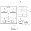
도 2는 본 발명의 일 실시 예에 따른 전자 장치를 나타낸다.
도 3은 다양한 실시 예에 따른 전자 장치 일부분의 단면도이다.
도 4는 다양한 실시 예에 따른 회로 패턴의 구성을 설명하기 위한 디지타이저의 분해 사시도이다.
도 5는 다양한 실시 예에 따른 격자 모양의 회로 패턴의 구성을 나타낸다.
도 6은 다양한 실시 예에 따른 마름모 모양의 회로 패턴의 구성을 나타낸다.
도 7은 다양한 실시 예에 따른 네트워크 환경 내의 전자 장치를 나타낸다.
도 8은 다양한 실시 예에 따른 전자 장치의 블록도이다.
도 9는 다양한 실시 예에 따른 프로그램 모듈의 블록도이다.
Claims (14)
- 전자 장치에 있어서,
표시 패널 하부에 배치되는 반사 시트;
상기 반사 시트 하부에 배치되는 디지타이저;를 포함하고,
상기 디지타이저는
제1 방향의 도전성 회로 패턴으로 구성된 제1 회로층;
제2 방향의 도전성 회로 패턴으로 구성된 제2 회로층; 및
상기 제1 회로층 및 상기 제2 회로층을 전기적으로 분리하는 절연층;을 포함하고,
상기 제1 회로층 또는 상기 제2 회로층 중 적어도 하나에 형성된 더미 회로 패턴;을 포함하는 전자 장치. - 청구항 1에 있어서,
상기 도전성 회로들은 루프(loop)를 형성하고,
상기 더미 회로들은 루프를 형성하지 않는 전자 장치. - 청구항 1에 있어서,
상기 더미 회로들은 상기 도전성 회로들과 동일하거나 또는 지정된 오차 범위 내의 높이 또는 두께 중 적어도 하나를 갖도록 구성되는 전자 장치. - 청구항 1에 있어서,
상기 더미 회로들은 상기 도전성 회로들과 일정한 간격으로 형성되는 전자 장치. - 청구항 1에 있어서,
상기 더미 회로들은 상기 더미 회로들을 구성하는 인접한 두 개의 더미 라인의 간격이 지정된 더미 회로 패턴과 지정된 도전성 회로 패턴 사이의 간격과 동일하거나 또는 지정된 오차 범위 내의 차이로 형성되는 전자 장치. - 청구항 1에 있어서,
상기 더미 회로들은 상기 더미 회로들을 구성하는 인접한 두 개의 더미 라인의 간격이 상기 도전성 회로들을 구성하는 인접한 두 개의 회로 라인의 간격과 동일하거나 또는 지정된 오차 범위 내의 차이로 형성되는 전자 장치. - 청구항 1에 있어서,
상기 도전성 회로 패턴은 세로축 또는 가로축 방향의 직선 모양인 적어도 하나의 회로 라인이 일정한 간격으로 반복적으로 구성된 형태이고,
상기 더미 회로 패턴은 상기 회로 라인과 같은 방향의 직선 모양인 적어도 하나의 더미 라인이 일정한 간격으로 반복적으로 구성된 형태인 전자 장치. - 청구항 1에 있어서,
상기 도전성 회로 패턴은 적어도 하나의 형상을 포함하고, 상기 도전성 회로 패턴은 상기 형상이 일정한 간격으로 반복적으로 구성된 형태이고,
상기 더미 회로 패턴은 상기 형상 내부에 적어도 하나의 상기 더미 회로들이 일정한 간격으로 구성된 형태인 전자 장치. - 청구항 8에 있어서,
상기 더미 회로들을 구성하는 더미 라인들은 적어도 한 번 꺾인 꺾은선 모양이며,
적어도 하나가 같은 방향으로 꺾이거나 또는 반대 방향으로 꺾여 서로 감싸는 형태로 구성되는 전자 장치. - 청구항 8에 있어서,
상기 더미 회로들을 구성하는 더미 라인들은 적어도 하나가 적어도 한 번 꺾인 꺾은선 모양이고, 나머지 적어도 하나가 직선 모양이며,
상기 직선 모양의 적어도 하나의 더미 라인이 상기 꺾은선 모양의 더미 라인의 적어도 하나의 변과 평행하게 구성되는 전자 장치. - 청구항 8에 있어서,
상기 더미 회로들을 구성하는 더미 라인들은 직선 모양이며, 상기 형상의 적어도 하나의 변과 평행하게 구성되는 전자 장치. - 전자 장치에 있어서,
상기 전자 장치의 외관을 형성하는 케이스;
상기 케이스에 안착되는 표시 패널;
상기 표시 패널 하부에 배치되는 반사시트; 및
상기 케이스와 상기 반사시트 사이에 배치되는 디지타이저;를 포함하고,
상기 디지타이저는
제1 방향의 도전성 회로 패턴으로 구성된 제1 회로층;
제2 방향의 도전성 회로 패턴으로 구성된 제2 회로층; 및
상기 제1 회로층 및 상기 제2 회로층을 전기적으로 분리하는 절연층;을 포함하고,
상기 제1 회로층 또는 상기 제2 회로층 중 적어도 하나에 형성되며, 상기 도전성 회로 패턴의 도전성 회로들과 형성되는 간격이 균일하게 형성되는 적어도 하나의 더미 회로;를 포함하는 전자 장치. - 전자 장치에 있어서,
표시 패널 하부에 배치되는 반사 시트; 및
상기 반사 시트 하부에 배치되는 디지타이저;를 포함하고,
상기 디지타이저는
절연층을 포함하고;
상기 절연층의 적어도 한 면에 도전성 회로 패턴 및 더미 회로 패턴을 포함하는 전자장치 - 청구항 13에 있어서,
상기 도전성 회로 패턴 및 상기 더미 회로 패턴은 상기 반사 시트와 인접한 면에 구성되는 전자 장치.
Priority Applications (4)
| Application Number | Priority Date | Filing Date | Title |
|---|---|---|---|
| KR1020150035304A KR102318028B1 (ko) | 2015-03-13 | 2015-03-13 | 디지타이저 회로 패터닝 방법 및 이를 지원하는 전자 장치 |
| US15/064,012 US10310644B2 (en) | 2015-03-13 | 2016-03-08 | Digitizer circuit patterning method and electronic device supporting the same |
| EP16159992.3A EP3067786B1 (en) | 2015-03-13 | 2016-03-11 | Digitizer circuit patterning method and electronic device supporting the same |
| CN201610144714.9A CN105975118B (zh) | 2015-03-13 | 2016-03-14 | 数字化电路图案化方法和支持其的电子装置 |
Applications Claiming Priority (1)
| Application Number | Priority Date | Filing Date | Title |
|---|---|---|---|
| KR1020150035304A KR102318028B1 (ko) | 2015-03-13 | 2015-03-13 | 디지타이저 회로 패터닝 방법 및 이를 지원하는 전자 장치 |
Publications (2)
| Publication Number | Publication Date |
|---|---|
| KR20160109964A true KR20160109964A (ko) | 2016-09-21 |
| KR102318028B1 KR102318028B1 (ko) | 2021-10-27 |
Family
ID=55527872
Family Applications (1)
| Application Number | Title | Priority Date | Filing Date |
|---|---|---|---|
| KR1020150035304A Active KR102318028B1 (ko) | 2015-03-13 | 2015-03-13 | 디지타이저 회로 패터닝 방법 및 이를 지원하는 전자 장치 |
Country Status (4)
| Country | Link |
|---|---|
| US (1) | US10310644B2 (ko) |
| EP (1) | EP3067786B1 (ko) |
| KR (1) | KR102318028B1 (ko) |
| CN (1) | CN105975118B (ko) |
Cited By (9)
| Publication number | Priority date | Publication date | Assignee | Title |
|---|---|---|---|---|
| KR20200115942A (ko) * | 2019-03-29 | 2020-10-08 | 삼성디스플레이 주식회사 | 표시 장치 |
| WO2022173137A1 (ko) * | 2021-02-09 | 2022-08-18 | 삼성전자 주식회사 | 디지타이저 패널 및 디지타이저 패널을 포함하는 전자 장치 |
| KR20220117173A (ko) * | 2021-02-16 | 2022-08-23 | 동우 화인켐 주식회사 | 디지타이저 및 이를 포함하는 화상 표시 장치 |
| US11500506B2 (en) | 2020-05-14 | 2022-11-15 | Samsung Display Co., Ltd. | Display device including a digitizer with reduced wiring visibility |
| WO2023200074A1 (ko) * | 2022-04-15 | 2023-10-19 | 삼성전자 주식회사 | 디스플레이를 포함하는 전자 장치 |
| US12166912B2 (en) | 2020-09-16 | 2024-12-10 | Samsung Display Co., Ltd. | Electronic apparatus including a lower member and a sensing sensor with openings overlapping a folding area |
| US12360562B2 (en) | 2021-02-09 | 2025-07-15 | Samsung Electronics Co., Ltd. | Digitizer panel and electronic device including the same |
| US12429916B2 (en) | 2022-04-15 | 2025-09-30 | Samsung Electronics Co., Ltd. | Electronic device including display |
| WO2025206582A1 (ko) * | 2024-03-26 | 2025-10-02 | 삼성전자주식회사 | 전자기 유도 패널을 포함하는 디스플레이 및 이를 포함하는 전자 장치 |
Families Citing this family (10)
| Publication number | Priority date | Publication date | Assignee | Title |
|---|---|---|---|---|
| US10895883B2 (en) * | 2016-08-26 | 2021-01-19 | Ademco Inc. | HVAC controller with a temperature sensor mounted on a flex circuit |
| US10838528B2 (en) * | 2017-03-14 | 2020-11-17 | Panasonic Intellectual Property Management Co., Ltd. | Touch panel and design structure provided with same |
| CN110402194B (zh) | 2017-03-14 | 2022-04-29 | 松下知识产权经营株式会社 | 触摸传感器 |
| WO2018227514A1 (zh) | 2017-06-16 | 2018-12-20 | 深圳市汇顶科技股份有限公司 | 指纹图像处理方法、光学指纹辨识系统及电子装置 |
| CN107507531A (zh) * | 2017-10-15 | 2017-12-22 | 张四清 | 一种新型的智能led显示屏 |
| CN108376038B (zh) * | 2018-01-18 | 2020-11-20 | 深圳市志凌伟业技术股份有限公司 | 可饶式透明基板做单面架桥sito触控面板制造方法 |
| CN109085949B (zh) * | 2018-07-27 | 2021-08-03 | 上海天马微电子有限公司 | 一种阵列基板及显示装置 |
| CN109378337A (zh) * | 2018-12-04 | 2019-02-22 | 广东速美达自动化股份有限公司 | 一种具有无线充电功能的oled屏幕及无线充电系统 |
| KR20220049066A (ko) * | 2020-10-13 | 2022-04-21 | 삼성디스플레이 주식회사 | 표시 장치 |
| KR20220085864A (ko) * | 2020-12-15 | 2022-06-23 | 삼성디스플레이 주식회사 | 표시 장치 |
Citations (4)
| Publication number | Priority date | Publication date | Assignee | Title |
|---|---|---|---|---|
| JP2012043219A (ja) * | 2010-08-19 | 2012-03-01 | Sony Corp | タッチ検出機能付き表示装置、および電子機器 |
| KR20130009608A (ko) * | 2011-07-14 | 2013-01-23 | 가부시키가이샤 와코무 | 위치 검출 센서 및 위치 검출 장치 |
| JP2014191650A (ja) * | 2013-03-27 | 2014-10-06 | Japan Display Inc | タッチ検出機能付き表示装置及び電子機器 |
| KR20140132879A (ko) * | 2013-05-08 | 2014-11-19 | 삼성디스플레이 주식회사 | 액정 표시 장치 |
Family Cites Families (14)
| Publication number | Priority date | Publication date | Assignee | Title |
|---|---|---|---|---|
| US5506375A (en) * | 1993-02-22 | 1996-04-09 | Wacom Co., Ltd. | Circuit board for coordinate detecting apparatus with noise suppression |
| US6756970B2 (en) * | 1998-11-20 | 2004-06-29 | Microsoft Corporation | Pen-based computer system |
| US7265303B2 (en) * | 2003-12-17 | 2007-09-04 | Microsoft Corporation | Electromagnetic digitizer sensor array |
| EP1746488A2 (en) | 2005-07-21 | 2007-01-24 | TPO Displays Corp. | Electromagnetic digitizer sensor array structure |
| JP4945483B2 (ja) * | 2008-02-27 | 2012-06-06 | 株式会社 日立ディスプレイズ | 表示パネル |
| JP4720857B2 (ja) * | 2008-06-18 | 2011-07-13 | ソニー株式会社 | 静電容量型入力装置および入力機能付き表示装置 |
| US8654092B2 (en) | 2009-01-26 | 2014-02-18 | Sharp Kabushiki Kaisha | Touch panel incorporating display device |
| US9651812B1 (en) * | 2009-12-04 | 2017-05-16 | Cypress Semiconductor Corporation | Partially filled contact and trace layout |
| JP5647864B2 (ja) * | 2010-11-05 | 2015-01-07 | 富士フイルム株式会社 | タッチパネル |
| JP5659073B2 (ja) * | 2011-04-22 | 2015-01-28 | 株式会社ジャパンディスプレイ | タッチ検出器付き表示パネル、および電子機器 |
| JP6117620B2 (ja) * | 2012-06-07 | 2017-04-19 | 日東電工株式会社 | タッチパネル部材及びその製造方法 |
| KR102068341B1 (ko) | 2013-07-10 | 2020-01-21 | 삼성디스플레이 주식회사 | 터치 스크린 패널 일체형 표시장치 |
| JP6266263B2 (ja) * | 2013-08-09 | 2018-01-24 | 株式会社ジャパンディスプレイ | タッチパネル及びタッチパネルを備えた液晶表示装置 |
| US9952691B2 (en) * | 2014-05-09 | 2018-04-24 | Lg Innotek Co., Ltd. | Touch panel and image display device having the same |
-
2015
- 2015-03-13 KR KR1020150035304A patent/KR102318028B1/ko active Active
-
2016
- 2016-03-08 US US15/064,012 patent/US10310644B2/en active Active
- 2016-03-11 EP EP16159992.3A patent/EP3067786B1/en not_active Not-in-force
- 2016-03-14 CN CN201610144714.9A patent/CN105975118B/zh not_active Expired - Fee Related
Patent Citations (4)
| Publication number | Priority date | Publication date | Assignee | Title |
|---|---|---|---|---|
| JP2012043219A (ja) * | 2010-08-19 | 2012-03-01 | Sony Corp | タッチ検出機能付き表示装置、および電子機器 |
| KR20130009608A (ko) * | 2011-07-14 | 2013-01-23 | 가부시키가이샤 와코무 | 위치 검출 센서 및 위치 검출 장치 |
| JP2014191650A (ja) * | 2013-03-27 | 2014-10-06 | Japan Display Inc | タッチ検出機能付き表示装置及び電子機器 |
| KR20140132879A (ko) * | 2013-05-08 | 2014-11-19 | 삼성디스플레이 주식회사 | 액정 표시 장치 |
Cited By (12)
| Publication number | Priority date | Publication date | Assignee | Title |
|---|---|---|---|---|
| KR20200115942A (ko) * | 2019-03-29 | 2020-10-08 | 삼성디스플레이 주식회사 | 표시 장치 |
| WO2020204247A1 (ko) * | 2019-03-29 | 2020-10-08 | 삼성디스플레이 주식회사 | 표시 장치 |
| US11966553B2 (en) | 2019-03-29 | 2024-04-23 | Samsung Display Co., Ltd. | Display device including digitizer |
| US11500506B2 (en) | 2020-05-14 | 2022-11-15 | Samsung Display Co., Ltd. | Display device including a digitizer with reduced wiring visibility |
| US11914833B2 (en) | 2020-05-14 | 2024-02-27 | Samsung Display Co., Ltd. | Display device |
| US12166912B2 (en) | 2020-09-16 | 2024-12-10 | Samsung Display Co., Ltd. | Electronic apparatus including a lower member and a sensing sensor with openings overlapping a folding area |
| WO2022173137A1 (ko) * | 2021-02-09 | 2022-08-18 | 삼성전자 주식회사 | 디지타이저 패널 및 디지타이저 패널을 포함하는 전자 장치 |
| US12360562B2 (en) | 2021-02-09 | 2025-07-15 | Samsung Electronics Co., Ltd. | Digitizer panel and electronic device including the same |
| KR20220117173A (ko) * | 2021-02-16 | 2022-08-23 | 동우 화인켐 주식회사 | 디지타이저 및 이를 포함하는 화상 표시 장치 |
| WO2023200074A1 (ko) * | 2022-04-15 | 2023-10-19 | 삼성전자 주식회사 | 디스플레이를 포함하는 전자 장치 |
| US12429916B2 (en) | 2022-04-15 | 2025-09-30 | Samsung Electronics Co., Ltd. | Electronic device including display |
| WO2025206582A1 (ko) * | 2024-03-26 | 2025-10-02 | 삼성전자주식회사 | 전자기 유도 패널을 포함하는 디스플레이 및 이를 포함하는 전자 장치 |
Also Published As
| Publication number | Publication date |
|---|---|
| US10310644B2 (en) | 2019-06-04 |
| CN105975118A (zh) | 2016-09-28 |
| EP3067786B1 (en) | 2018-12-05 |
| CN105975118B (zh) | 2021-02-02 |
| US20160266692A1 (en) | 2016-09-15 |
| EP3067786A1 (en) | 2016-09-14 |
| KR102318028B1 (ko) | 2021-10-27 |
Similar Documents
| Publication | Publication Date | Title |
|---|---|---|
| KR102318028B1 (ko) | 디지타이저 회로 패터닝 방법 및 이를 지원하는 전자 장치 | |
| KR102735206B1 (ko) | 지문 센서에 입력되는 노이즈를 감소시키는 장치 | |
| US20210349624A1 (en) | Method for setting date and time by electronic device and electronic device therefor | |
| KR102587736B1 (ko) | 카메라 모듈, 카메라 모듈이 적용된 전자 장치 및 이의 운용 방법 | |
| KR102499120B1 (ko) | 안테나를 포함하는 전자 장치 | |
| KR102401285B1 (ko) | 디스플레이를 포함하는 전자 장치 | |
| KR102622021B1 (ko) | 지문 센서를 갖는 전자 장치 | |
| KR102348486B1 (ko) | 전자 장치 | |
| KR102752942B1 (ko) | 디스플레이에 통합된 생체 센서를 포함하는 전자장치 | |
| KR102340480B1 (ko) | 전자 장치 및 전자 장치의 제어 방법 | |
| KR20180128178A (ko) | 콘텐츠를 표시하기 위한 방법 및 그 전자 장치 | |
| KR20180031511A (ko) | 가이드를 통해 지문 정보를 입력받는 장치 및 방법 | |
| KR20180063633A (ko) | 디스플레이를 포함하는 전자 장치 및 디스플레이의 제조 방법 | |
| KR20170112494A (ko) | 안테나 장치를 포함하는 전자 장치 | |
| KR20180001384A (ko) | 생체 센서 및 생체 센서를 포함하는 전자 장치 | |
| KR20180079978A (ko) | 터치 정확도 향상을 위한 터치 센서의 배치 방법 및 상기 방법을 이용한 전자 장치 | |
| KR102890456B1 (ko) | 디스플레이에 포함된 픽셀을 이용하여 센서의 위치를 확인하는 방법 및 전자 장치 | |
| KR20170040643A (ko) | 복수의 디스플레이를 구비한 전자장치 및 그 제어 방법 | |
| KR20170105892A (ko) | 적어도 일부가 구형의 일부로 마련되는 디스플레이 및 이를 포함하는 전자 장치 | |
| KR20160041208A (ko) | 플렉서블 디스플레이를 포함하는 전자 장치 | |
| KR20180123395A (ko) | 디스플레이에 통합된 압력 센서를 포함하는 전자장치 | |
| KR20170102681A (ko) | 전자 장치 및 그의 동작 방법 | |
| KR20170105330A (ko) | 터치 패널 및 이를 포함하는 전자 장치 | |
| US11192339B2 (en) | Touch screen display and electronic device including same | |
| KR102465149B1 (ko) | 표시 장치 및 이를 포함하는 전자 장치 |
Legal Events
| Date | Code | Title | Description |
|---|---|---|---|
| PA0109 | Patent application |
Patent event code: PA01091R01D Comment text: Patent Application Patent event date: 20150313 |
|
| PG1501 | Laying open of application | ||
| A201 | Request for examination | ||
| PA0201 | Request for examination |
Patent event code: PA02012R01D Patent event date: 20200228 Comment text: Request for Examination of Application Patent event code: PA02011R01I Patent event date: 20150313 Comment text: Patent Application |
|
| E902 | Notification of reason for refusal | ||
| PE0902 | Notice of grounds for rejection |
Comment text: Notification of reason for refusal Patent event date: 20210315 Patent event code: PE09021S01D |
|
| E701 | Decision to grant or registration of patent right | ||
| PE0701 | Decision of registration |
Patent event code: PE07011S01D Comment text: Decision to Grant Registration Patent event date: 20210819 |
|
| GRNT | Written decision to grant | ||
| PR0701 | Registration of establishment |
Comment text: Registration of Establishment Patent event date: 20211021 Patent event code: PR07011E01D |
|
| PR1002 | Payment of registration fee |
Payment date: 20211022 End annual number: 3 Start annual number: 1 |
|
| PG1601 | Publication of registration | ||
| PR1001 | Payment of annual fee |
Payment date: 20240927 Start annual number: 4 End annual number: 4 |