KR20160120004A - 시스템 온-칩 및 이를 포함하는 전자 기기 - Google Patents
시스템 온-칩 및 이를 포함하는 전자 기기 Download PDFInfo
- Publication number
- KR20160120004A KR20160120004A KR1020150048921A KR20150048921A KR20160120004A KR 20160120004 A KR20160120004 A KR 20160120004A KR 1020150048921 A KR1020150048921 A KR 1020150048921A KR 20150048921 A KR20150048921 A KR 20150048921A KR 20160120004 A KR20160120004 A KR 20160120004A
- Authority
- KR
- South Korea
- Prior art keywords
- initialization
- address range
- memory
- local
- random access
- Prior art date
- Legal status (The legal status is an assumption and is not a legal conclusion. Google has not performed a legal analysis and makes no representation as to the accuracy of the status listed.)
- Ceased
Links
Images


Classifications
-
- G—PHYSICS
- G06—COMPUTING OR CALCULATING; COUNTING
- G06F—ELECTRIC DIGITAL DATA PROCESSING
- G06F12/00—Accessing, addressing or allocating within memory systems or architectures
- G06F12/02—Addressing or allocation; Relocation
- G06F12/06—Addressing a physical block of locations, e.g. base addressing, module addressing, memory dedication
- G06F12/0607—Interleaved addressing
-
- G—PHYSICS
- G06—COMPUTING OR CALCULATING; COUNTING
- G06F—ELECTRIC DIGITAL DATA PROCESSING
- G06F12/00—Accessing, addressing or allocating within memory systems or architectures
- G06F12/02—Addressing or allocation; Relocation
- G06F12/0223—User address space allocation, e.g. contiguous or non contiguous base addressing
-
- G—PHYSICS
- G06—COMPUTING OR CALCULATING; COUNTING
- G06F—ELECTRIC DIGITAL DATA PROCESSING
- G06F15/00—Digital computers in general; Data processing equipment in general
- G06F15/76—Architectures of general purpose stored program computers
- G06F15/78—Architectures of general purpose stored program computers comprising a single central processing unit
- G06F15/7807—System on chip, i.e. computer system on a single chip; System in package, i.e. computer system on one or more chips in a single package
- G06F15/781—On-chip cache; Off-chip memory
-
- G—PHYSICS
- G06—COMPUTING OR CALCULATING; COUNTING
- G06F—ELECTRIC DIGITAL DATA PROCESSING
- G06F12/00—Accessing, addressing or allocating within memory systems or architectures
- G06F12/02—Addressing or allocation; Relocation
- G06F12/06—Addressing a physical block of locations, e.g. base addressing, module addressing, memory dedication
- G06F12/0646—Configuration or reconfiguration
- G06F12/0653—Configuration or reconfiguration with centralised address assignment
-
- G—PHYSICS
- G06—COMPUTING OR CALCULATING; COUNTING
- G06F—ELECTRIC DIGITAL DATA PROCESSING
- G06F12/00—Accessing, addressing or allocating within memory systems or architectures
- G06F12/02—Addressing or allocation; Relocation
- G06F12/08—Addressing or allocation; Relocation in hierarchically structured memory systems, e.g. virtual memory systems
- G06F12/0802—Addressing of a memory level in which the access to the desired data or data block requires associative addressing means, e.g. caches
- G06F12/0891—Addressing of a memory level in which the access to the desired data or data block requires associative addressing means, e.g. caches using clearing, invalidating or resetting means
-
- G—PHYSICS
- G06—COMPUTING OR CALCULATING; COUNTING
- G06F—ELECTRIC DIGITAL DATA PROCESSING
- G06F13/00—Interconnection of, or transfer of information or other signals between, memories, input/output devices or central processing units
- G06F13/14—Handling requests for interconnection or transfer
- G06F13/16—Handling requests for interconnection or transfer for access to memory bus
- G06F13/1605—Handling requests for interconnection or transfer for access to memory bus based on arbitration
- G06F13/1647—Handling requests for interconnection or transfer for access to memory bus based on arbitration with interleaved bank access
-
- G—PHYSICS
- G06—COMPUTING OR CALCULATING; COUNTING
- G06F—ELECTRIC DIGITAL DATA PROCESSING
- G06F13/00—Interconnection of, or transfer of information or other signals between, memories, input/output devices or central processing units
- G06F13/14—Handling requests for interconnection or transfer
- G06F13/16—Handling requests for interconnection or transfer for access to memory bus
- G06F13/1668—Details of memory controller
-
- G—PHYSICS
- G06—COMPUTING OR CALCULATING; COUNTING
- G06F—ELECTRIC DIGITAL DATA PROCESSING
- G06F15/00—Digital computers in general; Data processing equipment in general
- G06F15/76—Architectures of general purpose stored program computers
- G06F15/78—Architectures of general purpose stored program computers comprising a single central processing unit
- G06F15/7839—Architectures of general purpose stored program computers comprising a single central processing unit with memory
- G06F15/7842—Architectures of general purpose stored program computers comprising a single central processing unit with memory on one IC chip (single chip microcontrollers)
- G06F15/7857—Architectures of general purpose stored program computers comprising a single central processing unit with memory on one IC chip (single chip microcontrollers) using interleaved memory
-
- G—PHYSICS
- G11—INFORMATION STORAGE
- G11C—STATIC STORES
- G11C11/00—Digital stores characterised by the use of particular electric or magnetic storage elements; Storage elements therefor
- G11C11/21—Digital stores characterised by the use of particular electric or magnetic storage elements; Storage elements therefor using electric elements
- G11C11/34—Digital stores characterised by the use of particular electric or magnetic storage elements; Storage elements therefor using electric elements using semiconductor devices
- G11C11/40—Digital stores characterised by the use of particular electric or magnetic storage elements; Storage elements therefor using electric elements using semiconductor devices using transistors
- G11C11/401—Digital stores characterised by the use of particular electric or magnetic storage elements; Storage elements therefor using electric elements using semiconductor devices using transistors forming cells needing refreshing or charge regeneration, i.e. dynamic cells
- G11C11/4063—Auxiliary circuits, e.g. for addressing, decoding, driving, writing, sensing or timing
- G11C11/407—Auxiliary circuits, e.g. for addressing, decoding, driving, writing, sensing or timing for memory cells of the field-effect type
- G11C11/4072—Circuits for initialization, powering up or down, clearing memory or presetting
-
- G—PHYSICS
- G11—INFORMATION STORAGE
- G11C—STATIC STORES
- G11C7/00—Arrangements for writing information into, or reading information out from, a digital store
- G11C7/10—Input/output [I/O] data interface arrangements, e.g. I/O data control circuits, I/O data buffers
- G11C7/1072—Input/output [I/O] data interface arrangements, e.g. I/O data control circuits, I/O data buffers for memories with random access ports synchronised on clock signal pulse trains, e.g. synchronous memories, self timed memories
-
- G—PHYSICS
- G11—INFORMATION STORAGE
- G11C—STATIC STORES
- G11C7/00—Arrangements for writing information into, or reading information out from, a digital store
- G11C7/20—Memory cell initialisation circuits, e.g. when powering up or down, memory clear, latent image memory
-
- G—PHYSICS
- G06—COMPUTING OR CALCULATING; COUNTING
- G06F—ELECTRIC DIGITAL DATA PROCESSING
- G06F2212/00—Indexing scheme relating to accessing, addressing or allocation within memory systems or architectures
- G06F2212/20—Employing a main memory using a specific memory technology
- G06F2212/206—Memory mapped I/O
-
- G—PHYSICS
- G06—COMPUTING OR CALCULATING; COUNTING
- G06F—ELECTRIC DIGITAL DATA PROCESSING
- G06F2212/00—Indexing scheme relating to accessing, addressing or allocation within memory systems or architectures
- G06F2212/25—Using a specific main memory architecture
- G06F2212/253—Centralized memory
-
- Y—GENERAL TAGGING OF NEW TECHNOLOGICAL DEVELOPMENTS; GENERAL TAGGING OF CROSS-SECTIONAL TECHNOLOGIES SPANNING OVER SEVERAL SECTIONS OF THE IPC; TECHNICAL SUBJECTS COVERED BY FORMER USPC CROSS-REFERENCE ART COLLECTIONS [XRACs] AND DIGESTS
- Y02—TECHNOLOGIES OR APPLICATIONS FOR MITIGATION OR ADAPTATION AGAINST CLIMATE CHANGE
- Y02D—CLIMATE CHANGE MITIGATION TECHNOLOGIES IN INFORMATION AND COMMUNICATION TECHNOLOGIES [ICT], I.E. INFORMATION AND COMMUNICATION TECHNOLOGIES AIMING AT THE REDUCTION OF THEIR OWN ENERGY USE
- Y02D10/00—Energy efficient computing, e.g. low power processors, power management or thermal management
Landscapes
- Engineering & Computer Science (AREA)
- Theoretical Computer Science (AREA)
- General Engineering & Computer Science (AREA)
- Physics & Mathematics (AREA)
- General Physics & Mathematics (AREA)
- Computer Hardware Design (AREA)
- Microelectronics & Electronic Packaging (AREA)
- Computing Systems (AREA)
- Memory System Of A Hierarchy Structure (AREA)
- Stored Programmes (AREA)
Abstract
Description
도 2는 도 1의 전자 기기가 스마트폰으로 구현되는 일 예를 나타내는 도면이다.
도 3은 도 1의 전자 기기의 랜덤 액세스 메모리 장치에 포함된 랜덤 액세스 메모리의 일 예를 나타내는 블록도이다.
도 4는 본 발명의 실시예들에 따른 랜덤 액세스 메모리 장치를 나타내는 블록도이다.
도 5는 본 발명의 실시예들에 따른 시스템 온-칩을 나타내는 블록도이다.
도 6은 도 5의 시스템 온-칩이 수행하는 초기화 대상 메모리에 대한 초기화 동작을 설명하기 위한 도면이다.
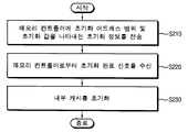
도 7은 도 5의 시스템 온-칩에 포함된 메모리 컨트롤러가 동작하는 일 예를 나타내는 순서도이다.
도 8은 도 5의 시스템 온-칩에 포함된 중앙 처리 장치가 동작하는 일 예를 나타내는 순서도이다.
도 9는 도 5의 시스템 온-칩이 초기화 대상 메모리에 대한 초기화 동작을 수행하는 일 예를 나타내는 도면이다.
도 10은 본 발명의 실시예들에 따른 랜덤 액세스 메모리 장치를 나타내는 블록도이다.
도 11은 본 발명의 실시예들에 따른 시스템 온-칩을 나타내는 블록도이다.
도 12는 도 11의 시스템 온-칩이 수행하는 초기화 대상 메모리에 대한 초기화 동작을 설명하기 위한 도면이다.
도 13은 도 11의 시스템 온-칩에 포함된 메모리 컨트롤러가 동작하는 일 예를 나타내는 순서도이다.
도 14는 도 11의 시스템 온-칩에 포함된 중앙 처리 장치가 동작하는 일 예를 나타내는 순서도이다.
도 15는 도 11의 시스템 온-칩에 의해 초기화 대상 메모리에 대한 초기화 동작이 수행되는 일 예를 나타내는 도면이다.
도 16은 도 11의 시스템 온-칩에 의해 기능 장치의 초기화 어드레스 범위로의 액세스 요청이 처리되는 일 예를 나타내는 순서도이다.
도 17은 도 11의 시스템 온-칩에 의해 기능 장치의 초기화 어드레스 범위로의 액세스 요청이 처리되는 일 예를 나타내는 도면이다.
도 18은 본 발명의 실시예들에 따른 컴퓨팅 시스템을 나타내는 블록도이다.
120: 기능 장치 130: 랜덤 액세스 메모리 장치
131: 메모리 컨트롤러 132: 랜덤 액세스 메모리
133: 트래픽 인터리버 140: 파워 서플라이
500: 컴퓨팅 시스템 510: 프로세서
520: 입출력 허브 530: 입출력 컨트롤러 허브
540: 랜덤 메모리 장치들 550: 그래픽 카드
Claims (20)
- 적어도 하나 이상의 중앙 처리 장치; 및
상기 중앙 처리 장치로부터 초기화 어드레스 범위 및 초기화 값을 나타내는 초기화 정보를 수신하고, 상기 초기화 정보에 기초하여 적어도 하나 이상의 초기화 대상 메모리 및 상기 초기화 대상 메모리의 로컬 초기화 어드레스 범위를 결정하며, 상기 초기화 대상 메모리에 상기 초기화 값으로 이루어진 초기화 데이터를 기 설정된 단위로 전송함으로써 상기 초기화 대상 메모리의 상기 로컬 초기화 어드레스 범위를 초기화시키는 메모리 컨트롤러를 포함하는 시스템 온-칩. - 제 1 항에 있어서, 상기 기 설정된 단위는 상기 로컬 초기화 어드레스 범위보다 작게 설정되고, 상기 메모리 컨트롤러는 상기 초기화 대상 메모리에 상기 초기화 데이터를 반복적으로 전송하는 시스템 온-칩.
- 제 1 항에 있어서, 상기 기 설정된 단위는 상기 로컬 초기화 어드레스 범위로 설정되고, 상기 메모리 컨트롤러는 상기 초기화 대상 메모리에 상기 초기화 데이터를 한 번에 전송하는 시스템 온-칩.
- 제 1 항에 있어서, 상기 초기화 대상 메모리의 상기 로컬 초기화 어드레스 범위가 초기화되어 로컬 초기화 완료 신호가 상기 초기화 대상 메모리로부터 모두 수신되면, 상기 메모리 컨트롤러는 상기 중앙 처리 장치에 초기화 완료 신호를 전송하는 시스템 온-칩.
- 제 4 항에 있어서, 상기 초기화 완료 신호가 상기 메모리 컨트롤러로부터 수신되면, 상기 중앙 처리 장치는 내부 캐시를 초기화시키는 시스템 온-칩.
- 제 1 항에 있어서, 상기 초기화 정보가 상기 중앙 처리 장치로부터 수신되면, 상기 메모리 컨트롤러는 외부 장치의 상기 초기화 어드레스 범위로의 액세스 요청에 대한 처리를 보류시키는 시스템 온-칩.
- 제 6 항에 있어서, 상기 초기화 대상 메모리의 상기 로컬 초기화 어드레스 범위가 초기화되어 로컬 초기화 완료 신호가 상기 초기화 대상 메모리로부터 모두 수신되면, 상기 메모리 컨트롤러는 상기 액세스 요청에 대한 상기 처리를 재개시키는 시스템 온-칩.
- 적어도 하나 이상의 중앙 처리 장치;
상기 중앙 처리 장치로부터 초기화 어드레스 범위 및 초기화 값을 나타내는 초기화 정보를 수신하고, 상기 초기화 정보에 기초하여 적어도 하나 이상의 초기화 대상 메모리 및 상기 초기화 대상 메모리의 로컬 초기화 어드레스 범위를 결정하며, 상기 초기화 대상 메모리의 상기 로컬 초기화 어드레스 범위 및 상기 초기화 값을 나타내는 로컬 초기화 정보를 생성하는 트래픽 인터리버; 및
적어도 하나 이상의 랜덤 액세스 메모리를 포함하는 랜덤 액세스 메모리 그룹들 각각을 제어하되, 상기 트래픽 인터리버로부터 상기 로컬 초기화 정보를 수신하고, 상기 로컬 초기화 정보에 기초하여 상기 초기화 대상 메모리에 상기 초기화 값으로 이루어진 초기화 데이터를 기 설정된 단위로 전송함으로써 상기 초기화 대상 메모리의 상기 로컬 초기화 어드레스 범위를 초기화시키는 메모리 컨트롤러들을 포함하는 시스템 온-칩. - 제 8 항에 있어서, 상기 기 설정된 단위는 상기 로컬 초기화 어드레스 범위보다 작게 설정되고, 상기 메모리 컨트롤러들은 상기 초기화 대상 메모리에 상기 초기화 데이터를 반복적으로 전송하는 시스템 온-칩.
- 제 8 항에 있어서, 상기 기 설정된 단위는 상기 로컬 초기화 어드레스 범위로 설정되고, 상기 메모리 컨트롤러들은 상기 초기화 대상 메모리에 상기 초기화 데이터를 한 번에 전송하는 시스템 온-칩.
- 제 8 항에 있어서, 상기 초기화 대상 메모리의 상기 로컬 초기화 어드레스 범위가 초기화되어 로컬 초기화 완료 신호가 상기 초기화 대상 메모리로부터 상기 메모리 컨트롤러를 거쳐 모두 수신되면, 상기 트래픽 인터리버는 상기 중앙 처리 장치에 초기화 완료 신호를 전송하는 시스템 온-칩.
- 제 11 항에 있어서, 상기 초기화 완료 신호가 상기 트래픽 인터리버로부터 수신되면, 상기 중앙 처리 장치는 내부 캐시를 초기화시키는 시스템 온-칩.
- 제 8 항에 있어서, 상기 초기화 정보가 상기 중앙 처리 장치로부터 수신되면, 상기 트래픽 인터리버는 외부 장치의 상기 초기화 어드레스 범위로의 액세스 요청에 대한 처리를 보류시키는 시스템 온-칩.
- 제 13 항에 있어서, 상기 초기화 대상 메모리의 상기 로컬 초기화 어드레스 범위가 초기화되어 로컬 초기화 완료 신호가 상기 초기화 대상 메모리로부터 상기 메모리 컨트롤러를 거쳐 모두 수신되면, 상기 트래픽 인터리버는 상기 액세스 요청에 대한 상기 처리를 재개시키는 시스템 온-칩.
- 초기화 어드레스 범위 및 초기화 값을 나타내는 초기화 정보를 수신하고, 상기 초기화 정보에 기초하여 적어도 하나 이상의 초기화 대상 메모리의 로컬 초기화 어드레스 범위를 결정하며, 상기 초기화 대상 메모리에 상기 초기화 값으로 이루어진 초기화 데이터를 기 설정된 단위로 전송함으로써 상기 초기화 대상 메모리의 상기 로컬 초기화 어드레스 범위를 초기화시키는 랜덤 액세스 메모리 장치; 및
상기 랜덤 액세스 메모리 장치를 제어하되, 상기 랜덤 액세스 메모리 장치의 상기 초기화 어드레스 범위를 초기화시키기 위한 상기 초기화 정보를 상기 랜덤 액세스 메모리 장치에 제공하는 적어도 하나 이상의 중앙 처리 장치를 포함하는 전자 기기. - 제 15 항에 있어서, 상기 기 설정된 단위는 상기 로컬 초기화 어드레스 범위보다 작게 설정되고, 상기 초기화 데이터는 상기 초기화 대상 메모리에 반복적으로 전송되는 전자 기기.
- 제 15 항에 있어서, 상기 기 설정된 단위는 상기 로컬 초기화 어드레스 범위로 설정되고, 상기 초기화 데이터는 상기 초기화 대상 메모리에 한 번에 전송되는 전자 기기.
- 제 15 항에 있어서, 상기 초기화 대상 메모리의 상기 로컬 초기화 어드레스 범위가 모두 초기화되면, 상기 랜덤 액세스 메모리 장치는 상기 중앙 처리 장치에 초기화 완료 신호를 전송하는 전자 기기.
- 제 18 항에 있어서, 상기 초기화 완료 신호가 상기 랜덤 액세스 메모리 장치로부터 수신되면, 상기 중앙 처리 장치는 내부 캐시를 초기화시키는 전자 기기.
- 제 15 항에 있어서, 상기 초기화 정보가 상기 중앙 처리 장치로부터 수신되면, 상기 랜덤 액세스 메모리 장치는 상기 중앙 처리 장치의 상기 초기화 어드레스 범위로의 액세스 요청에 대한 처리를 보류시키고, 상기 초기화 대상 메모리의 상기 로컬 초기화 어드레스 범위가 모두 초기화되면, 상기 랜덤 액세스 메모리 장치는 상기 액세스 요청에 대한 상기 처리를 재개시키는 전자 기기.
Priority Applications (3)
| Application Number | Priority Date | Filing Date | Title |
|---|---|---|---|
| KR1020150048921A KR20160120004A (ko) | 2015-04-07 | 2015-04-07 | 시스템 온-칩 및 이를 포함하는 전자 기기 |
| US14/995,804 US10409722B2 (en) | 2015-04-07 | 2016-01-14 | System on-chip and electronic device including the same |
| CN201610195645.4A CN106055516B (zh) | 2015-04-07 | 2016-03-31 | 片上系统和包括其的电子装置以及将存储器初始化的方法 |
Applications Claiming Priority (1)
| Application Number | Priority Date | Filing Date | Title |
|---|---|---|---|
| KR1020150048921A KR20160120004A (ko) | 2015-04-07 | 2015-04-07 | 시스템 온-칩 및 이를 포함하는 전자 기기 |
Publications (1)
| Publication Number | Publication Date |
|---|---|
| KR20160120004A true KR20160120004A (ko) | 2016-10-17 |
Family
ID=57111379
Family Applications (1)
| Application Number | Title | Priority Date | Filing Date |
|---|---|---|---|
| KR1020150048921A Ceased KR20160120004A (ko) | 2015-04-07 | 2015-04-07 | 시스템 온-칩 및 이를 포함하는 전자 기기 |
Country Status (3)
| Country | Link |
|---|---|
| US (1) | US10409722B2 (ko) |
| KR (1) | KR20160120004A (ko) |
| CN (1) | CN106055516B (ko) |
Cited By (2)
| Publication number | Priority date | Publication date | Assignee | Title |
|---|---|---|---|---|
| KR20190133175A (ko) * | 2017-03-31 | 2019-12-02 | 암, 리미티드 | 스토리지 디바이스의 초기화 |
| KR20220090928A (ko) * | 2020-12-23 | 2022-06-30 | 삼성전자주식회사 | 시스템 온 칩 테스트 방법 및 시스템 온 칩 테스트 시스템 |
Families Citing this family (2)
| Publication number | Priority date | Publication date | Assignee | Title |
|---|---|---|---|---|
| CN111209232B (zh) | 2018-11-21 | 2022-04-22 | 昆仑芯(北京)科技有限公司 | 访问静态随机存取存储器的方法、装置、设备和存储介质 |
| CN112069112B (zh) * | 2020-09-04 | 2022-08-19 | 龙芯中科技术股份有限公司 | Uart控制器配置方法和系统 |
Family Cites Families (24)
| Publication number | Priority date | Publication date | Assignee | Title |
|---|---|---|---|---|
| US5878240A (en) * | 1995-05-11 | 1999-03-02 | Lucent Technologies, Inc. | System and method for providing high speed memory access in a multiprocessor, multimemory environment |
| JP3821911B2 (ja) | 1997-05-02 | 2006-09-13 | 富士通株式会社 | メモリ初期化制御方式 |
| JPH11259356A (ja) | 1998-03-06 | 1999-09-24 | Fujitsu Ltd | メモリ初期化装置 |
| US6154821A (en) | 1998-03-10 | 2000-11-28 | Rambus Inc. | Method and apparatus for initializing dynamic random access memory (DRAM) devices by levelizing a read domain |
| JP2001175496A (ja) | 1999-12-16 | 2001-06-29 | Nec Shizuoka Ltd | メモリ制御回路 |
| US6857041B2 (en) * | 2002-03-29 | 2005-02-15 | Intel Corporation | Method and apparatus providing an interface to allow physical memory to be initialized using firmware/hardware methods |
| KR100585136B1 (ko) | 2004-03-04 | 2006-05-30 | 삼성전자주식회사 | 메모리 시스템의 데이터 채널 초기화 방법 |
| US7143220B2 (en) * | 2004-03-10 | 2006-11-28 | Intel Corporation | Apparatus and method for granting concurrent ownership to support heterogeneous agents in on-chip busses having different grant-to-valid latencies |
| JP2006021407A (ja) * | 2004-07-07 | 2006-01-26 | Konica Minolta Business Technologies Inc | 画像形成装置および画像形成装置の制御方法 |
| US7210030B2 (en) * | 2004-07-22 | 2007-04-24 | International Business Machines Corporation | Programmable memory initialization system and method |
| KR100564635B1 (ko) | 2004-10-25 | 2006-03-28 | 삼성전자주식회사 | 메모리 모듈 내에서의 인터페이스 타이밍을 제어하는메모리 시스템 및 그 방법 |
| US7464243B2 (en) | 2004-12-21 | 2008-12-09 | Cisco Technology, Inc. | Method and apparatus for arbitrarily initializing a portion of memory |
| US7290094B2 (en) * | 2005-05-17 | 2007-10-30 | International Business Machines Corporation | Processor, data processing system, and method for initializing a memory block to an initialization value without a cache first obtaining a data valid copy |
| WO2008016081A1 (en) * | 2006-08-04 | 2008-02-07 | Panasonic Corporation | Memory controller, nonvolatile memory device, access device, and nonvolatile memory system |
| US7809885B2 (en) * | 2006-09-29 | 2010-10-05 | Voom Technologies, Inc. | Scalable hard-drive replicator |
| US8271604B2 (en) * | 2006-12-19 | 2012-09-18 | International Business Machines Corporation | Initializing shared memories for sharing endpoints across a plurality of root complexes |
| US8006032B2 (en) | 2007-08-22 | 2011-08-23 | Globalfoundries Inc. | Optimal solution to control data channels |
| US20090089515A1 (en) * | 2007-10-02 | 2009-04-02 | Qualcomm Incorporated | Memory Controller for Performing Memory Block Initialization and Copy |
| JP4901968B2 (ja) * | 2010-03-01 | 2012-03-21 | 株式会社東芝 | 半導体記憶装置 |
| EP2579159B1 (en) | 2010-05-27 | 2015-05-06 | Fujitsu Limited | Memory system, memory device, and memory interface device |
| US8856482B2 (en) * | 2011-03-11 | 2014-10-07 | Micron Technology, Inc. | Systems, devices, memory controllers, and methods for memory initialization |
| CN102567245B (zh) * | 2011-12-27 | 2014-10-01 | 深圳国微技术有限公司 | 用于soc芯片系统的存储控制器及其实现方法 |
| US9607714B2 (en) * | 2012-12-26 | 2017-03-28 | Nvidia Corporation | Hardware command training for memory using write leveling mechanism |
| US9575884B2 (en) * | 2013-05-13 | 2017-02-21 | Qualcomm Incorporated | System and method for high performance and low cost flash translation layer |
-
2015
- 2015-04-07 KR KR1020150048921A patent/KR20160120004A/ko not_active Ceased
-
2016
- 2016-01-14 US US14/995,804 patent/US10409722B2/en active Active
- 2016-03-31 CN CN201610195645.4A patent/CN106055516B/zh active Active
Cited By (2)
| Publication number | Priority date | Publication date | Assignee | Title |
|---|---|---|---|---|
| KR20190133175A (ko) * | 2017-03-31 | 2019-12-02 | 암, 리미티드 | 스토리지 디바이스의 초기화 |
| KR20220090928A (ko) * | 2020-12-23 | 2022-06-30 | 삼성전자주식회사 | 시스템 온 칩 테스트 방법 및 시스템 온 칩 테스트 시스템 |
Also Published As
| Publication number | Publication date |
|---|---|
| CN106055516B (zh) | 2021-08-27 |
| US10409722B2 (en) | 2019-09-10 |
| US20160299842A1 (en) | 2016-10-13 |
| CN106055516A (zh) | 2016-10-26 |
Similar Documents
| Publication | Publication Date | Title |
|---|---|---|
| US12518818B2 (en) | Method of performing internal processing operation of memory device | |
| KR102401271B1 (ko) | 메모리 시스템 및 그 동작 방법 | |
| KR102238652B1 (ko) | 데이터 저장 장치, 이의 작동 방법, 및 이를 포함하는 데이터 처리 시스템의 작동 방법 | |
| US9472258B2 (en) | Method of operating memory device and method of operating memory system including the same | |
| US9772803B2 (en) | Semiconductor memory device and memory system | |
| US9336851B2 (en) | Memory device and method of refreshing in a memory device | |
| JP5537533B2 (ja) | ハードウェアのダイナミックなキャッシュパワー管理 | |
| US10976933B2 (en) | Storage device, storage system and method of operating the same | |
| US11631448B1 (en) | Memory device performing refresh operation and method of operating the same | |
| US20130111102A1 (en) | Semiconductor memory devices | |
| US20170194045A1 (en) | Semiconductor memory devices and memory systems including the same | |
| US20140237177A1 (en) | Memory module and memory system having the same | |
| US9064603B1 (en) | Semiconductor memory device and memory system including the same | |
| US9449673B2 (en) | Memory device and memory system having the same | |
| US10445261B2 (en) | System memory having point-to-point link that transports compressed traffic | |
| CN106055516B (zh) | 片上系统和包括其的电子装置以及将存储器初始化的方法 | |
| US20160314758A1 (en) | UEFI Virtual Video Controller | |
| US20180052787A1 (en) | Memory system supporting an offset command | |
| US10853255B2 (en) | Apparatus and method of optimizing memory transactions to persistent memory using an architectural data mover | |
| US12093528B2 (en) | System and method for managing data access in distributed systems | |
| US20170075571A1 (en) | Memory device and control method thereof | |
| CN121100327A (zh) | 用于存储器设备的灵活元数据区 | |
| US20140331006A1 (en) | Semiconductor memory devices | |
| US8006029B2 (en) | DDR flash implementation with direct register access to legacy flash functions | |
| US12494239B2 (en) | Apparatuses and methods for providing command having on-the-fly (OTF) latency to memory |
Legal Events
| Date | Code | Title | Description |
|---|---|---|---|
| PA0109 | Patent application |
Patent event code: PA01091R01D Comment text: Patent Application Patent event date: 20150407 |
|
| PG1501 | Laying open of application | ||
| A201 | Request for examination | ||
| PA0201 | Request for examination |
Patent event code: PA02012R01D Patent event date: 20200316 Comment text: Request for Examination of Application Patent event code: PA02011R01I Patent event date: 20150407 Comment text: Patent Application |
|
| E902 | Notification of reason for refusal | ||
| PE0902 | Notice of grounds for rejection |
Comment text: Notification of reason for refusal Patent event date: 20211111 Patent event code: PE09021S01D |
|
| E601 | Decision to refuse application | ||
| PE0601 | Decision on rejection of patent |
Patent event date: 20220210 Comment text: Decision to Refuse Application Patent event code: PE06012S01D Patent event date: 20211111 Comment text: Notification of reason for refusal Patent event code: PE06011S01I |