KR20160136070A - Light emitting device - Google Patents
Light emitting device Download PDFInfo
- Publication number
- KR20160136070A KR20160136070A KR1020150069775A KR20150069775A KR20160136070A KR 20160136070 A KR20160136070 A KR 20160136070A KR 1020150069775 A KR1020150069775 A KR 1020150069775A KR 20150069775 A KR20150069775 A KR 20150069775A KR 20160136070 A KR20160136070 A KR 20160136070A
- Authority
- KR
- South Korea
- Prior art keywords
- electrode
- pattern
- semiconductor layer
- light emitting
- connection groove
- Prior art date
- Legal status (The legal status is an assumption and is not a legal conclusion. Google has not performed a legal analysis and makes no representation as to the accuracy of the status listed.)
- Granted
Links
Images










Classifications
-
- H—ELECTRICITY
- H10—SEMICONDUCTOR DEVICES; ELECTRIC SOLID-STATE DEVICES NOT OTHERWISE PROVIDED FOR
- H10H—INORGANIC LIGHT-EMITTING SEMICONDUCTOR DEVICES HAVING POTENTIAL BARRIERS
- H10H20/00—Individual inorganic light-emitting semiconductor devices having potential barriers, e.g. light-emitting diodes [LED]
- H10H20/80—Constructional details
- H10H20/83—Electrodes
- H10H20/831—Electrodes characterised by their shape
- H10H20/8314—Electrodes characterised by their shape extending at least partially onto an outer side surface of the bodies
-
- H01L33/36—
-
- H01L33/12—
-
- H—ELECTRICITY
- H10—SEMICONDUCTOR DEVICES; ELECTRIC SOLID-STATE DEVICES NOT OTHERWISE PROVIDED FOR
- H10H—INORGANIC LIGHT-EMITTING SEMICONDUCTOR DEVICES HAVING POTENTIAL BARRIERS
- H10H20/00—Individual inorganic light-emitting semiconductor devices having potential barriers, e.g. light-emitting diodes [LED]
- H10H20/80—Constructional details
- H10H20/83—Electrodes
- H10H20/831—Electrodes characterised by their shape
- H10H20/8312—Electrodes characterised by their shape extending at least partially through the bodies
-
- H—ELECTRICITY
- H10—SEMICONDUCTOR DEVICES; ELECTRIC SOLID-STATE DEVICES NOT OTHERWISE PROVIDED FOR
- H10H—INORGANIC LIGHT-EMITTING SEMICONDUCTOR DEVICES HAVING POTENTIAL BARRIERS
- H10H20/00—Individual inorganic light-emitting semiconductor devices having potential barriers, e.g. light-emitting diodes [LED]
- H10H20/80—Constructional details
- H10H20/83—Electrodes
- H10H20/831—Electrodes characterised by their shape
- H10H20/8316—Multi-layer electrodes comprising at least one discontinuous layer
-
- H—ELECTRICITY
- H10—SEMICONDUCTOR DEVICES; ELECTRIC SOLID-STATE DEVICES NOT OTHERWISE PROVIDED FOR
- H10H—INORGANIC LIGHT-EMITTING SEMICONDUCTOR DEVICES HAVING POTENTIAL BARRIERS
- H10H20/00—Individual inorganic light-emitting semiconductor devices having potential barriers, e.g. light-emitting diodes [LED]
- H10H20/80—Constructional details
- H10H20/85—Packages
- H10H20/857—Interconnections, e.g. lead-frames, bond wires or solder balls
-
- H01L2924/12041—
-
- H—ELECTRICITY
- H10—SEMICONDUCTOR DEVICES; ELECTRIC SOLID-STATE DEVICES NOT OTHERWISE PROVIDED FOR
- H10H—INORGANIC LIGHT-EMITTING SEMICONDUCTOR DEVICES HAVING POTENTIAL BARRIERS
- H10H20/00—Individual inorganic light-emitting semiconductor devices having potential barriers, e.g. light-emitting diodes [LED]
- H10H20/01—Manufacture or treatment
- H10H20/032—Manufacture or treatment of electrodes
-
- H—ELECTRICITY
- H10—SEMICONDUCTOR DEVICES; ELECTRIC SOLID-STATE DEVICES NOT OTHERWISE PROVIDED FOR
- H10H—INORGANIC LIGHT-EMITTING SEMICONDUCTOR DEVICES HAVING POTENTIAL BARRIERS
- H10H20/00—Individual inorganic light-emitting semiconductor devices having potential barriers, e.g. light-emitting diodes [LED]
- H10H20/80—Constructional details
- H10H20/81—Bodies
- H10H20/811—Bodies having quantum effect structures or superlattices, e.g. tunnel junctions
- H10H20/812—Bodies having quantum effect structures or superlattices, e.g. tunnel junctions within the light-emitting regions, e.g. having quantum confinement structures
-
- H—ELECTRICITY
- H10—SEMICONDUCTOR DEVICES; ELECTRIC SOLID-STATE DEVICES NOT OTHERWISE PROVIDED FOR
- H10H—INORGANIC LIGHT-EMITTING SEMICONDUCTOR DEVICES HAVING POTENTIAL BARRIERS
- H10H20/00—Individual inorganic light-emitting semiconductor devices having potential barriers, e.g. light-emitting diodes [LED]
- H10H20/80—Constructional details
- H10H20/81—Bodies
- H10H20/819—Bodies characterised by their shape, e.g. curved or truncated substrates
- H10H20/82—Roughened surfaces, e.g. at the interface between epitaxial layers
-
- H—ELECTRICITY
- H10—SEMICONDUCTOR DEVICES; ELECTRIC SOLID-STATE DEVICES NOT OTHERWISE PROVIDED FOR
- H10H—INORGANIC LIGHT-EMITTING SEMICONDUCTOR DEVICES HAVING POTENTIAL BARRIERS
- H10H20/00—Individual inorganic light-emitting semiconductor devices having potential barriers, e.g. light-emitting diodes [LED]
- H10H20/80—Constructional details
- H10H20/81—Bodies
- H10H20/822—Materials of the light-emitting regions
- H10H20/824—Materials of the light-emitting regions comprising only Group III-V materials, e.g. GaP
- H10H20/825—Materials of the light-emitting regions comprising only Group III-V materials, e.g. GaP containing nitrogen, e.g. GaN
-
- H—ELECTRICITY
- H10—SEMICONDUCTOR DEVICES; ELECTRIC SOLID-STATE DEVICES NOT OTHERWISE PROVIDED FOR
- H10H—INORGANIC LIGHT-EMITTING SEMICONDUCTOR DEVICES HAVING POTENTIAL BARRIERS
- H10H20/00—Individual inorganic light-emitting semiconductor devices having potential barriers, e.g. light-emitting diodes [LED]
- H10H20/80—Constructional details
- H10H20/83—Electrodes
- H10H20/832—Electrodes characterised by their material
- H10H20/835—Reflective materials
-
- H—ELECTRICITY
- H10—SEMICONDUCTOR DEVICES; ELECTRIC SOLID-STATE DEVICES NOT OTHERWISE PROVIDED FOR
- H10H—INORGANIC LIGHT-EMITTING SEMICONDUCTOR DEVICES HAVING POTENTIAL BARRIERS
- H10H20/00—Individual inorganic light-emitting semiconductor devices having potential barriers, e.g. light-emitting diodes [LED]
- H10H20/80—Constructional details
- H10H20/84—Coatings, e.g. passivation layers or antireflective coatings
Landscapes
- Led Devices (AREA)
Abstract
Description
본 발명 실시 예는 발광 소자에 관한 것이다.Embodiments of the present invention relate to a light emitting device.
발광 다이오드(Light Emitting Diode: LED)는 전류가 인가되면 광을 방출하는 발광 소자 중 하나이다. 발광 다이오드는 저 전압으로 고효율의 광을 방출할 수 있어 에너지 절감 효과가 뛰어나다. 최근, 발광 다이오드의 휘도 문제가 크게 개선되어, 액정 표시 장치의 백라이트 유닛(Backlight Unit), 전광판, 표시기, 가전 제품 등과 같은 각종 기기에 적용되고 있다.A light emitting diode (LED) is one of light emitting devices that emits light when current is applied. The light emitting diode is capable of emitting light with high efficiency at a low voltage, thus providing excellent energy saving effect. In recent years, the problem of luminance of a light emitting diode has been greatly improved, and it has been applied to various devices such as a backlight unit of a liquid crystal display device, a display board, a display device, and a home appliance.
발광 소자는 지지 기판 상에 배치되는 제 1 반도체층, 활성층, 및 제 2 반도체층을 포함하는 발광 구조물을 포함하며, 발광 구조물과 접속되는 제 1 전극과 제 2 전극을 포함한다. 상기와 같은 발광 소자는 제 1 전극을 통해 주입되는 전자 또는 정공과 제 2 전극을 통해 주입되는 정공 또는 전자는 제 1 전극과 제 2 전극의 전압 차이에 의해 이동하여 활성층에서 만나 발광한다.The light emitting device includes a light emitting structure including a first semiconductor layer, an active layer, and a second semiconductor layer disposed on a support substrate, and includes a first electrode and a second electrode connected to the light emitting structure. In the light emitting device, the electrons or holes injected through the first electrode and the holes or electrons injected through the second electrode move due to a voltage difference between the first electrode and the second electrode, and emit light in the active layer.
그런데, 발광 구조물에 형성된 접속 홈 내부에서 제 2 반도체층과 전기적으로 연결되는 제 2 전극을 형성하고, 절연 패턴을 통해 제 2 전극과 제 1 반도체층을 절연시키는 수직형 발광 소자는 공정 마진에 의해 제 1 전극의 끝단과 제 2 전극의 끝단이 이격된 구조를 갖는다. 그런데, 제 1 전극과 제 2 전극의 간격이 넓어질수록 발광 소자의 구동 전압이 증가하고 광 출력이 저하되는 문제가 발생한다.The vertical light emitting device which forms the second electrode electrically connected to the second semiconductor layer in the connection groove formed in the light emitting structure and insulates the second electrode and the first semiconductor layer through the insulating pattern is formed by the process margin And a structure in which an end of the first electrode and an end of the second electrode are spaced apart from each other. However, as the distance between the first electrode and the second electrode increases, the driving voltage of the light emitting device increases and the light output decreases.
본 발명 실시 예는 구동 전압을 감소시키고 광 출력을 향상시킬 수 있는 발광 소자를 제공한다.The embodiment of the present invention provides a light emitting device capable of reducing the driving voltage and improving the light output.
실시 예의 발광 소자는 지지 기판; 상기 지지 기판 상에 배치되며, 제 1 반도체층, 활성층 및 제 2 반도체층을 포함하는 발광 구조물; 상기 발광 구조물이 제거되어 상기 제 2 반도체층을 노출시키는 바닥면과 상기 제 1 반도체층, 활성층 및 제 2 반도체층을 노출시키는 측면을 포함하는 복수 개의 접속 홈; 상기 제 1 반도체층과 접촉하도록 상기 발광 구조물 상에 배치되며, 끝단이 상기 접속 홈의 가장자리까지 연장된 제 1 전극 패턴 및 상기 제 1 전극 패턴 상에 배치된 제 2 전극 패턴을 포함하는 제 1 전극; 상기 접속 홈의 바닥면 및 측면을 감싸도록 상기 제 1 반도체층의 상부면까지 연장된 콘택 전극 및 복수 개의 상기 콘택 전극과 연결된 본딩 전극을 포함하는 제 2 전극; 및 상기 제 1 전극과 상기 제 2 전극 사이에 배치된 절연 패턴을 포함한다.The light emitting device of the embodiment includes a support substrate; A light emitting structure disposed on the supporting substrate, the light emitting structure including a first semiconductor layer, an active layer, and a second semiconductor layer; A plurality of connection grooves including a bottom surface from which the light emitting structure is removed to expose the second semiconductor layer and a side surface that exposes the first semiconductor layer, the active layer, and the second semiconductor layer; A first electrode pattern disposed on the light emitting structure so as to be in contact with the first semiconductor layer, the first electrode pattern having an end extending to an edge of the connection groove, and a second electrode pattern disposed on the first electrode pattern; ; A second electrode including a contact electrode extending to an upper surface of the first semiconductor layer so as to surround a bottom surface and a side surface of the connection groove, and a bonding electrode connected to the plurality of contact electrodes; And an insulating pattern disposed between the first electrode and the second electrode.
실시 예의 발광 소자는 지지 기판; 상기 지지 기판 상에 배치되며, 제 1 반도체층, 활성층 및 제 2 반도체층을 포함하는 발광 구조물; 상기 발광 구조물이 제거되어 상기 제 2 반도체층을 노출시키는 바닥면과 상기 제 1 반도체층, 활성층 및 제 2 반도체층을 노출시키는 측면을 포함하는 복수 개의 접속 홈; 상기 제 1 반도체층과 전기적으로 연결되며, 상기 접속 홈의 내부까지 연장된 제 1 전극 패턴 및 상기 제 1 전극 패턴 상에 배치된 제 2 전극 패턴을 포함하는 제 1 전극; 상기 접속 홈의 바닥면 및 측면을 감싸도록 상기 접속 홈의 가장자리까지 연장된 콘택 전극 및 복수 개의 상기 콘택 전극과 연결된 본딩 전극을 포함하는 제 2 전극; 및 상기 제 1 전극과 상기 제 2 전극 사이에 배치된 절연 패턴을 포함한다.The light emitting device of the embodiment includes a support substrate; A light emitting structure disposed on the supporting substrate, the light emitting structure including a first semiconductor layer, an active layer, and a second semiconductor layer; A plurality of connection grooves including a bottom surface from which the light emitting structure is removed to expose the second semiconductor layer and a side surface that exposes the first semiconductor layer, the active layer, and the second semiconductor layer; A first electrode electrically connected to the first semiconductor layer, the first electrode including a first electrode pattern extended to the inside of the connection groove and a second electrode pattern disposed on the first electrode pattern; A second electrode including a contact electrode extending to an edge of the connection groove and a bonding electrode connected to the plurality of contact electrodes so as to surround the bottom surface and the side surface of the connection groove; And an insulating pattern disposed between the first electrode and the second electrode.
실시 예에 따르면 본 발명 실시 예의 발광 소자는 다음과 같은 효과가 있다.According to the embodiment, the light emitting device of the embodiment of the present invention has the following effects.
첫째, 제 1 반도체층의 상부면에 형성되어 제 1 반도체층과 직접 접촉되는 제 1 전극의 제 1 전극 패턴은 접속 홈의 가장자리까지 형성된다. 즉, 반사층으로 기능하는 제 1 전극 패턴과 활성층의 중첩 면적이 넓어져 반사 효율이 향상되어 광 출력이 향상된다.First, the first electrode pattern of the first electrode formed on the upper surface of the first semiconductor layer and in direct contact with the first semiconductor layer is formed up to the edge of the connection groove. That is, the overlapping area of the first electrode pattern serving as the reflective layer and the active layer is widened, so that the reflection efficiency is improved and the light output is improved.
둘째, 접속 홈을 통해 제 2 반도체층과 직접 접촉되는 제 2 전극의 콘택 전극이 접속 홈의 내부 전면에 형성된다. 따라서, 콘택 전극과 제 2 반도체층의 접촉 면적이 넓어져 구동 전압이 감소한다.Second, the contact electrode of the second electrode, which is in direct contact with the second semiconductor layer through the connection groove, is formed on the entire inner surface of the connection groove. Therefore, the contact area between the contact electrode and the second semiconductor layer is widened, and the driving voltage is reduced.
셋째, 제 1 반도체층과 직접 접촉되는 제 1 전극의 제 1 전극 패턴과 제 2 반도체층과 직접 접촉되는 제 2 전극의 콘택 전극이 절연 패턴을 사이에 두고 중첩된다. 따라서, 제 1 전극 끝단과 제 2 전극 끝단의 간격이 0(zero)이 되어 발광 소자의 저항이 감소하고 발광 소자의 구동 전압 역시 감소한다.Third, the first electrode pattern of the first electrode directly contacting with the first semiconductor layer and the contact electrode of the second electrode directly contacting the second semiconductor layer are overlapped with each other with the insulating pattern interposed therebetween. Accordingly, the gap between the first electrode tip and the second electrode tip becomes 0 (zero), so that the resistance of the light emitting element decreases and the driving voltage of the light emitting element also decreases.
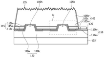
도 1a는 본 발명 실시 예의 발광 소자의 단면도이다.
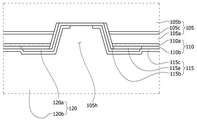
도 1b는 도 1a의 A 영역의 확대도이다.
도 2는 일반적인 발광 소자의 단면도이다.
도 3a는 제 1 전극과 제 2 전극의 간격에 따른 구동 전압을 나타낸 그래프이다.
도 3b는 제 1 전극과 제 2 전극의 간격에 따른 광 출력을 나타낸 그래프이다.
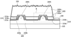
도 4a는 본 발명 다른 실시 예의 발광 소자의 단면도이다.
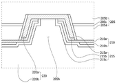
도 4b는 도 4a의 B 영역의 확대도이다.
도 5a 내지 도 5i는 본 발명 실시 예의 발광 소자의 제조 방법을 나타낸 공정 단면도이다.
도 6a 내지 도 6i는 본 발명 다른 실시 예의 발광 소자의 제조 방법을 나타낸 공정 단면도이다.
도 7은 본 발명 실시 예의 발광 소자를 포함하는 발광 소자 패키지의 단면도이다.1A is a cross-sectional view of a light emitting device according to an embodiment of the present invention.
1B is an enlarged view of region A of FIG. 1A.
2 is a cross-sectional view of a general light emitting device.
3A is a graph illustrating a driving voltage according to an interval between a first electrode and a second electrode.
3B is a graph illustrating light output according to the interval between the first electrode and the second electrode.
4A is a cross-sectional view of a light emitting device according to another embodiment of the present invention.
FIG. 4B is an enlarged view of the area B in FIG. 4A. FIG.
5A to 5I are process cross-sectional views illustrating a method of manufacturing a light emitting device of an embodiment of the present invention.
6A to 6I are process sectional views showing a method for manufacturing a light emitting device according to another embodiment of the present invention.
7 is a cross-sectional view of a light emitting device package including the light emitting device of the embodiment of the present invention.
본 발명은 다양한 변경을 가할 수 있고 여러 가지 실시 예를 가질 수 있는 바, 특정 실시 예를 도면에 예시하고 설명하고자 한다. 그러나, 이는 본 발명 실시 예를 특정한 실시 형태에 대해 한정하려는 것이 아니며, 실시 예의 사상 및 기술 범위에 포함되는 모든 변경, 균등물 내지 대체물을 포함하는 것으로 이해되어야 한다.While the invention is susceptible to various modifications and alternative forms, specific embodiments thereof are shown by way of example in the drawings and will herein be described in detail. It should be understood, however, that the embodiments of the present invention are not intended to be limited to the specific embodiments but include all modifications, equivalents, and alternatives falling within the spirit and scope of the embodiments.
제 1, 제 2 등과 같이 서수를 포함하는 용어는 다양한 구성 요소들을 설명하는데 사용될 수 있지만, 상기 구성 요소들은 상기 용어들에 의해 한정되지는 않는다. 상기 용어들은 하나의 구성 요소를 다른 구성 요소로부터 구별하는 목적으로만 사용된다. 예를 들어, 실시 예의 권리 범위를 벗어나지 않으면서 제 2 구성 요소는 제 1 구성 요소로 명명될 수 있고, 유사하게 제 1 구성 요소도 제 2 구성 요소로 명명될 수 있다. 및/또는 이라는 용어는 복수의 관련된 기재된 항목들의 조합 또는 복수의 관련된 기재된 항목들 중의 어느 항목을 포함한다.Terms including ordinals, such as first, second, etc., may be used to describe various elements, but the elements are not limited to these terms. The terms are used only for the purpose of distinguishing one component from another. For example, without departing from the scope of the embodiments, the second component may be referred to as a first component, and similarly, the first component may also be referred to as a second component. And / or < / RTI > includes any combination of a plurality of related listed items or any of a plurality of related listed items.
어떤 구성 요소가 다른 구성 요소에 "연결되어" 있다거나 "접속되어" 있다고 언급된 때에는, 그 다른 구성 요소에 직접적으로 연결되어 있거나 또는 접속되어 있을 수도 있지만, 중간에 다른 구성 요소가 존재할 수도 있다고 이해되어야 할 것이다. 반면에, 어떤 구성 요소가 다른 구성 요소에 "직접 연결되어" 있다거나 "직접 접속되어" 있다고 언급된 때에는, 중간에 다른 구성 요소가 존재하지 않는 것으로 이해되어야 할 것이다.It is to be understood that when an element is referred to as being "connected" or "connected" to another element, it may be directly connected or connected to the other element, . On the other hand, when an element is referred to as being "directly connected" or "directly connected" to another element, it should be understood that there are no other elements in between.
본 출원에서 사용한 용어는 단지 특정한 실시 예를 설명하기 위해 사용된 것으로, 본 발명 실시 예를 한정하려는 의도가 아니다. 단수의 표현은 문맥상 명백하게 다르게 뜻하지 않는 한, 복수의 표현을 포함한다. 본 출원에서, "포함하다" 또는 "가지다" 등의 용어는 명세서상에 기재된 특징, 숫자, 단계, 동작, 구성 요소, 부품 또는 이들을 조합한 것이 존재함을 지정하려는 것이지, 하나 또는 그 이상의 다른 특징들이나 숫자, 단계, 동작, 구성 요소, 부품 또는 이들을 조합한 것들의 존재 또는 부가 가능성을 미리 배제하지 않는 것으로 이해되어야 한다.The terminology used herein is for the purpose of describing particular embodiments only and is not intended to limit the embodiments of the invention. The singular expressions include plural expressions unless the context clearly dictates otherwise. In the present application, the terms "comprises" or "having" and the like are used to specify that there is a feature, a number, a step, an operation, an element, a component or a combination thereof described in the specification, But do not preclude the presence or addition of one or more other features, integers, steps, operations, elements, components, or combinations thereof.
실시 예의 설명에 있어서, 어느 한 구성 요소가 다른 구성 요소의 "상(위) 또는 하(아래)(on or under)"에 형성되는 것으로 기재되는 경우에 있어, 상(위) 또는 하(아래)(on or under)는 두 개의 구성 요소가 서로 직접(directly)접촉되거나 하나 이상의 다른 구성 요소가 상기 두 구성 요소 사이에 배치되어(indirectly) 형성되는 것을 모두 포함한다. 또한 "상(위) 또는 하(아래)(on or under)"으로 표현되는 경우 하나의 구성 요소를 기준으로 위쪽 방향뿐만 아니라 아래쪽 방향의 의미도 포함할 수 있다.In the description of the embodiments, when an element is described as being formed "on or under" another element, the upper or lower (lower) (on or under) all include that the two components are in direct contact with each other or that one or more other components are indirectly formed between the two components. Also, when expressed as "on or under", it may include not only an upward direction but also a downward direction with respect to one component.
이하, 첨부된 도면을 참조하여 실시 예를 상세히 설명하되, 도면 부호에 관계없이 동일하거나 대응하는 구성 요소는 동일한 참조 번호를 부여하고 이에 대한 중복되는 설명은 생략하기로 한다.Hereinafter, embodiments will be described in detail with reference to the accompanying drawings, wherein like or corresponding elements are denoted by the same reference numerals, and redundant description thereof will be omitted.
이하, 첨부된 도면을 참조하여 실시 예의 발광 소자를 상세히 설명하면 다음과 같다.Hereinafter, the light emitting device of the embodiment will be described in detail with reference to the accompanying drawings.
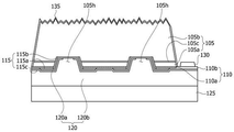
도 1a는 본 발명 실시 예의 발광 소자의 단면도이며, 도 1b는 도 1a의 A 영역의 확대도이다.1A is a cross-sectional view of a light emitting device according to an embodiment of the present invention, and FIG. 1B is an enlarged view of a region A of FIG. 1A.
도 1a 및 도 1b와 같이, 본 발명 실시 예의 발광 소자는 지지 기판(125) 상에 배치되며 제 1 반도체층(105a), 활성층(105c) 및 제 2 반도체층(105b)을 포함하는 발광 구조물(105), 제 1 반도체층(105a)과 전기적으로 연결된 제 1 전극(110), 제 2 반도체층(105b)과 전기적으로 연결된 제 2 전극(120), 제 1 전극(110)과 제 2 전극(120)을 절연시키는 절연 패턴(115)을 포함한다. 이 때, 제 1 반도체층(105a)과 직접 접촉되는 제 1 전극(110)의 제 1 전극 패턴(110a)과 제 2 반도체층(105b)과 직접 접촉되는 제 2 전극(120)의 콘택 전극(120a)은 절연 패턴(115)을 사이에 두고 제 1 반도체층(105a) 하부면에서 중첩된다.1A and 1B, the light emitting device of the embodiment of the present invention includes a light emitting structure (not shown) disposed on a
제 1 반도체층(105a)은 Ⅲ-Ⅴ족, Ⅱ-Ⅵ족 등의 화합물 반도체로 구현될 수 있으며, 제 1 반도체층(105a)에 제 1 도펀트가 도핑될 수 있다. 제 1 반도체층(105a)은 InxAlyGa1 -x- yN (0=x=1, 0=y=1, 0=x+y=1)의 조성식을 갖는 반도체 물질 또는 AlInN, AlGaAs, GaP, GaAs, GaAsP, AlGaInP 중 선택된 물질로 형성될 수 있다. 제 1 도펀트가 Mg, Zn, Ca, Sr, Ba 등과 같은 p형 도펀트인 경우, 제 1 도펀트가 도핑된 제 1 반도체층(105a)은 p형 반도체층일 수 있다. The
본 발명 실시 예의 발광 소자가 자외선, 심자외선(Deep UV) 또는 무분극 발광 소자일 경우, 제 1 반도체층(105a)은 InAlGaN 및 AlGaN 중 적어도 하나를 포함할 수 있다. 제 1 반도체층(105a)이 p형 반도체층일 경우, 제 1 반도체층(105a)은 격자 차이를 줄이기 위해 알루미늄의 농도가 구배를 갖는 graded AlGaN을 포함할 수 있다. 제 1 반도체층(105a)은 단층 또는 다층 구조일 수 있으며 도면에서는 단층 구조인 것을 도시하였다.When the light emitting device of the embodiment of the present invention is an ultraviolet ray, a deep ultraviolet ray (Deep UV), or a non-polarized light emitting device, the
활성층(105c)은 제 1 반도체층(105a)과 제 2 반도체층(105b) 사이에 배치된다. 활성층(105c)은 제 1 반도체층(105a)을 통해서 주입되는 전자(또는 정공)과 제 2 반도체층(105b)을 통해서 주입되는 정공(또는 전자)이 만나는 층이다. 활성층(105c)은 전자와 정공이 재결합함에 따라 낮은 에너지 준위로 천이하며, 그에 상응하는 파장을 가지는 빛을 생성할 수 있다.The
활성층(105c)은 단일 우물 구조, 다중 우물 구조, 단일 양자 우물 구조, 다중 양자 우물(Multi Quantum Well; MQW) 구조, 양자점 구조 또는 양자선 구조 중 어느 하나의 구조를 가질 수 있으며, 활성층(105c)의 구조는 이에 한정하지 않는다.The
활성층(105c)이 우물 구조로 형성되는 경우, 활성층(105c)의 우물층/장벽층은 InGaN/GaN, InGaN/InGaN, GaN/AlGaN, InAlGaN/GaN, GaAs(InGaAs)/AlGaAs, GaP(InGaP)/AlGaP 중 어느 하나 이상의 페어 구조로 형성될 수 있으나 이에 한정되지 않는다. 우물층은 장벽층의 밴드 갭보다 작은 밴드 갭을 갖는 물질로 형성될 수 있다.InGaN / InGaN, GaN / AlGaN, InAlGaN / GaN, GaAs (InGaAs) / AlGaAs, GaP (InGaP), and InGaN / InGaN / / AlGaP, but the present invention is not limited thereto. The well layer may be formed of a material having a band gap smaller than the band gap of the barrier layer.
제 2 반도체층(105b)은 Ⅲ-Ⅴ족, Ⅱ-Ⅵ족 등의 화합물 반도체로 구현될 수 있으며, 제 2 반도체층(105b)에 제 2 도펀트가 도핑될 수 있다. 제 2 반도체층(105b)은 AlxInyGa(1-x-y)N (0=x=1, 0=y=1, 0=x+y=1)의 조성식을 갖는 반도체 물질, InAlGaN, AlGaAs, GaP, GaAs, GaAsP, AlGaInP 중 어느 하나 이상으로 형성될 수 있으며, 이에 한정하지 않는다. 제 2 도펀트가 Si, Ge, Sn, Se, Te 등과 같은 n형 도펀트인 경우, 제 2 도펀트가 도핑된 제 2 반도체층(105b)은 n형 반도체층일 수 있다.The
본 발명 실시 예의 발광 소자가 자외선(UV), 심자외선(Deep UV) 또는 무분극 발광 소자일 경우, 제 2 반도체층(105b)은 InAlGaN 및 AlGaN 중 적어도 하나를 포함할 수 있다. 제 2 반도체층(105b)이 AlGaN으로 이루어질 경우 Al의 함량은 50%일 수 있다. 또한, 제 2 반도체층(105b)이 n형 반도체층인 경우, 제 2 반도체층(105b)은 Al0 .5GaN으로 이루어질 수 있다.When the light emitting element of the embodiment of the present invention is ultraviolet (UV), deep ultraviolet (Deep UV) or unpolarized light emitting device, the
도면에서는 단층의 제 2 반도체층(105b)을 도시하였으나, 제 2 반도체층(105b)은 다층 구조일 수 있다. 제 2 반도체층(105b)이 다층 구조인 경우, 제 2 반도체층(105b)은 언도프트 반도체층(미도시)을 더 포함할 수 있다. 언도프트 반도체층은 제 2 반도체층(105b)의 결정성 향상을 위해 형성되는 층으로, 언도프트 반도체층은 제 2 도펀트가 도핑되지 않아 제 2 반도체층(105b)에 비해 낮은 전기 전도성을 가질 수 있다.Although the single-layer
본 발명 실시 예의 발광 구조물(105)은 p형 반도체층인 제 1 반도체층(105a)과 n형 반도체층인 제 2 반도체층(105b)을 포함하여 이루어지거나, n형 반도체층인 제 1 반도체층(105a)과 p형 반도체층인 제 2 반도체층(105b)을 포함하여 이루어질 수 있다. 또한, 발광 구조물(105)은 제 2 반도체층(105b)과 활성층(105c) 사이에 n형 또는 p형 반도체층이 더 형성된 구조일 수 있다. 즉, 본 발명 실시 예의 발광 구조물(105)은 np, pn, npn, pnp 접합 구조 중 적어도 어느 하나의 구조로 형성될 수 있는 것으로, 본 발명 실시 예의 발광 구조물(105)은 n형 반도체층과 p형 반도체층을 포함하는 다양한 구조일 수 있다.The
그리고, 제 1 반도체층(105a) 및 제 2 반도체층(105b) 내의 불순물의 도핑 농도는 균일 또는 불균일하게 형성될 수 있다. 즉, 발광 구조물(105)의 도핑 구조는 다양하게 형성될 수 있으며, 이에 대해 한정하지는 않는다.The doping concentrations of the impurities in the
상기와 같은 발광 구조물(105)을 감싸도록 보호층(135)이 형성될 수 있다. 보호층(135)은 비전도성의 산화물이나 질화물로 이루어질 수 있다. 예를 들어, 보호층(135)은 SiO2, SixOy, Si3N4, SixNy, SiOxNy, Al2O3, TiO2, AlN 등으로 이루어진 군에서 적어도 하나가 선택되어 형성될 수 있으며, 이에 한정하지 않는다. 또한, 제 2 반도체층(105b)의 상부면이 러프니스 패턴을 가져, 보호층(135) 역시 러프니스 패턴을 따라 형성될 수 있다. 이 때, 러프니스 패턴은 도시된 바와 같이 불균일한 패턴이거나 균일한 패턴일 수 있다.The
제 1 전극(110)은 제 1 반도체층(105a)과 전기적으로 연결되고, 제 2 전극(120)은 제 2 반도체층(105b)과 전기적으로 연결된다. 이 때, 제 2 전극(120)은 제 1 반도체층(105a), 활성층(105c) 및 제 2 반도체층(105b)을 선택적으로 제거하여 제 2 반도체층(105b)을 노출시키는 복수 개의 접속 홈(105h)을 통해 제 2 반도체층(105b)과 접속된다.The
구체적으로, 제 1 전극(110)은 제 1 반도체층(105a)과 중첩되도록 발광 구조물(105)과 지지 기판(125) 사이에 형성될 수 있다. 제 1 전극(110)은 제 1 반도체층(105a)과 직접 접촉하는 제 1 전극 패턴(110a) 및 제 1 전극 패턴(110a)을 감싸도록 제 1 전극 패턴(110a) 하부에 배치된 제 2 전극 패턴(110b)을 포함한다. The
제 1 전극 패턴(110a)은 활성층(105c)에서 발생한 광을 제 2 반도체층(105b) 방향으로 반사시키기 위한 반사층으로 기능할 수 있다. 이를 위해, 제 1 전극 패턴(110a)은 Ag, Ni, Al, Rh, Pd, Ir, Ru, Mg, Zn, Pt, Au 및 Hf 등과 같이 반사율이 높은 물질로 형성되거나, 상기 반사율이 높은 물질과 IZO, IZTO, IAZO, IGZO, IGTO, AZO, ATO 등과 같은 투명 전도성 물질이 혼합되어 형성될 수 있다.The
제 1 전극 패턴(110a)은 제 1 반도체층(105a)과 직접 접촉하도록 발광 구조물(105) 하부에 배치되며, 끝단이 접속 홈(105h)의 가장자리까지 연장된다. 즉, 제 1 전극 패턴(110a)의 끝단이 접속 홈(105h)의 가장자리와 일치한다. 이 때, 제 1 전극 패턴(110a)은 반사층으로 기능한다. 따라서, 본 발명 실시 예의 발광 소자는 제 1 전극 패턴(110a)이 접속 홈(105h)을 제외한 제 1 반도체층(105a) 전면에 형성되어, 제 1 전극 패턴(110a)과 활성층(105c)의 중첩 면적이 넓어진다. 즉, 활성층(105c)에서 발생한 광의 반사 효율이 향상되어 발광 소자의 광 출력이 향상된다.The
제 2 전극 패턴(110b)은 외부로부터 주입된 전류가 수평적으로 골고루 퍼질 수 있도록 우수한 전기 전도성을 갖는 물질로 형성될 수 있다. 제 2 전극 패턴(110b)은 투명 전도성 산화막(Tranparent Conductive Oxide; TCO)으로 형성될 수 있다. 투명 전도성 산화막은 ITO(Indium Tin Oxide), IZO(Indium Zinc Oxide), AZO(Aluminum Zinc Oxide), AGZO(Aluminum Gallium Zinc Oxide), IZTO(Indium Zinc Tin Oxide), IAZO(Indium Aluminum Zinc Oxide), IGZO(Indium Gallium Zinc Oxide), IGTO(Indium Gallium Tin Oxide), ATO(Antimony Tin Oxide), GZO(Gallium Zinc Oxide), IZON(IZO Nitride), ZnO, IrOx, RuOx 및 NiO 등에서 선택될 수 있다.The
또한, 제 2 전극 패턴(110b)은 Ag, Ni, Al, Rh, Pd, Ir, Ru, Mg, Zn, Pt, Au, Hf 등과 같은 불투명 금속으로 형성될 수 있다. 또한, 제 2 전극 패턴(110b)은 투명 전도성 산화막과 불투명 금속이 혼합된 하나 또는 복수 개의 층으로 형성될 수 있으며, 이에 한정하지 않는다.The
발광 구조물(105)과 지지 기판(125) 사이에는 제 2 반도체층(105b)과 전기적으로 연결된 제 2 전극(120)이 배치된다. 제 2 전극(120)은 상술한 바와 같이 복수 개의 접속 홈(105h)을 통해 제 2 반도체층(105b)과 접속된다. 이 때, 접속 홈(105h)은 제 2 반도체층(105b)을 노출시키는 바닥면과 제 1 반도체층(105a), 활성층(105c) 및 제 2 반도체층(105b)을 노출시키는 측면을 포함한다.A
제 2 전극(120)은 접속 홈(105h)에서 제 2 반도체층(105b)과 접촉하는 콘택 전극(120a)과 각 콘택 전극(120a)을 연결시키는 본딩 전극(120b)을 포함한다. 콘택 전극(120a)은 접속 홈(105h)의 바닥면 및 측면을 완전히 감싸도록 제 1 반도체층(105a)의 하부면까지 배치된다. 즉, 콘택 전극(120a)은 접속 홈(105h) 내측면의 전면에 배치되어, 콘택 전극(120a)과 제 2 반도체층(105b)의 접촉 면적이 넓어진다. 따라서, 발광 소자의 구동 전압이 감소한다.The
도면에서는 본딩 전극(120b)이 단일 층인 것을 도시하였으나, 본딩 전극(120b)은 투명 전도성 산화막과 불투명 금속이 혼합된 하나 또는 복수 개의 층으로 형성될 수 있으며, 이에 한정하지 않는다.Although the
그리고, 상기와 같은 제 1 전극(110)과 제 2 전극(120) 사이에는 절연 패턴(115)이 배치되어, 제 1 전극(110)과 제 2 전극(120)을 전기적으로 절연시킬 수 있다. 절연 패턴(115)은 제 1, 제 2 및 제 3 절연 패턴(115a, 115b 및 115c)을 포함할 수 있다.An
제 1 절연 패턴(115a)은 제 1 반도체층(105a) 하부에서 콘택 전극(120a)과 제 1 전극 패턴(110a)을 절연시킨다. 따라서, 콘택 전극(120a)과 제 1 전극 패턴(110a)은 접속 홈(105h) 주변의 제 1 반도체층(105a) 하부면에서 제 1 절연 패턴(115a)을 사이에 두고 중첩된다. 이 때, 접속 홈(105h)의 가장자리에서 제 1 전극 패턴(110a)과 제 1 절연 패턴(115a)의 끝단이 일치한다.The
그리고, 제 2 절연 패턴(115b)은 접속 홈(105h)의 측면에 배치되며, 구체적으로, 콘택 전극(120a)과 접속 홈(105h)의 측면 사이에 배치된다. 제 2 절연 패턴(115b)은 접속 홈(105h)의 가장자리까지 연장된 콘택 전극(120a)의 끝단과 콘택 전극(120a)을 절연시킨다. 또한, 접속 홈(105h)의 측면에서 콘택 전극(120a)과 활성층(105c) 및 콘택 전극(120a)과 제 1 반도체층(105a)이 제 2 절연 패턴(115b)을 통해 서로 절연될 수 있다.The second
그리고, 제 3 절연 패턴(115c)은 발광 구조물(105) 하부에 배치되어, 본딩 전극(120b)과 제 2 전극 패턴(110b)을 절연시킨다. 구체적으로, 제 3 절연 패턴(115c)은 접속 홈(105h) 내부의 콘택 전극(120a)을 노출시키도록 제 1 전극(110) 하부면의 전면에 배치되고, 콘택 전극(120a)과 본딩 전극(120b)이 접속 홈(105h) 내부에서 전기적으로 연결될 수 있다.The third
상기와 같은 제 1, 제 2 및 제 3 절연 패턴(115a, 115b 및 115c)은 SiO2, SixOy, Si3N4, SixNy, SiOxNy, Al2O3, TiO2, AlN 등으로 이루어진 군에서 적어도 하나가 선택되어 형성될 수 있으며, 이에 한정하지 않는다.The first, second, and third
도시하지는 않았으나, 제 2 전극(120)은 본딩층(미도시)을 통해 지지 기판(125)과 전기적으로 연결될 수 있다. 본딩층은 Au, Sn, In, Ag, Ni, Nb, Cu 등과 같은 금속 또는 이들의 합금으로 형성될 수 있으며, 이에 한정되지 않는다. 또한, 본딩층은 지지 기판(125)과 제 2 전극(120)을 본딩 또는 웰딩(Welding) 본딩 또는 확산(diffusion) 본딩시킬 수 있다. 이 때, 본딩층은 고체 상태(solid state)로서, 전기적 전도성을 갖는 물질로 이루어질 수 있으나, 이에 한정하지 않는다.Although not shown, the
따라서, 지지 기판(125)은 발광 구조물(105)을 지지함과 동시에 제 2 전극(120)과 전기적으로 연결되어 제 2 전극(120)의 전극 패드로 기능할 수 있다. 그리고, 보호층(135)에 의해 노출된 제 1 전극(110) 상부면에 전극 패드(130)가 형성될 수 있다. 전극 패드(130)는 제 1 전극(110)과 전기적으로 연결된다.Accordingly, the supporting
상기와 같은 본 발명 실시 예의 발광 소자는 제 1 반도체층(105a)과 접촉되는 제 1 전극(110)의 제 1 전극 패턴(110a)과 제 2 반도체층(105b)과 접촉되는 제 2 전극(120)의 콘택 전극(120a)이 절연 패턴(115)을 사이에 두고 서로 중첩된다. 따라서, 제 1 전극(110) 끝단과 제 2 전극(120) 끝단의 간격이 0(zero)이되어, 발광 소자의 저항이 감소하여 구동 전압이 감소한다.The light emitting device of the present invention may include a
반면, 일반적인 발광 소자는 제 1 전극, 절연 패턴 및 제 2 전극의 공정 마진에 의해 제 1 전극의 끝단과 제 2 전극의 끝단이 최소 20㎛이상 이격 된다.On the other hand, in a typical light emitting device, the end of the first electrode and the end of the second electrode are spaced apart by at least 20 탆 at least due to the process margin of the first electrode, the insulation pattern, and the second electrode.
도 2는 일반적인 발광 소자의 단면도로, 접속 홈을 포함하는 발광 소자의 일부를 도시하였다.2 is a cross-sectional view of a general light emitting device, and shows a part of a light emitting device including a connection groove.
도 2와 같이, 일반적인 발광 소자는 제 1 전극(10a)이 발광 구조물(15) 상부에서 제 1 반도체층(15a)과 전기적으로 연결되고, 제 2 전극(12a)은 접속 홈 내부에서 제 2 반도체층(15b)과 전기적으로 연결된다. 그리고, 접속 홈 측면에 절연 패턴(11)이 배치되어 제 2 전극(12a)과 제 1 반도체층(15a)이 절연될 수 있다.2, in a general light emitting device, a
그런데, 상기와 같은 일반적인 발광 소자는 접속 홈(15h)의 바닥면의 일부를 노출시키도록 절연 패턴(11)을 형성하는 공정, 접속 홈(15h) 내부에서 절연 패턴(11)에 의해 노출된 제 2 반도체층(15b) 상부면에 제 2 전극(12a)을 형성하는 공정 및 제 1 반도체층(15a) 상에 제 1 전극(10a)을 형성하는 공정이 충분한 마진을 가져야 한다. 따라서, 일반적인 발광 소자는 제 1 전극(10a)의 끝단과 접속 홈(15h) 가장자리 사이의 간격(A) 및 제 2 전극(12a)의 끝단과 접속 홈(15h) 바닥면의 가장자리 사이의 간격(B)에 의해 제 1 전극(10a) 끝단과 제 2 전극(12a) 끝단의 간격이 최소 20㎛이상이다.The conventional light emitting device may include a step of forming an insulating
도 3a는 제 1 전극과 제 2 전극의 간격에 따른 구동 전압을 나타낸 그래프이며, 도 3b는 제 1 전극과 제 2 전극의 간격에 따른 광 출력을 나타낸 그래프이다. 도 3a 및 도 3b는 청색 광을 방출하는 발광 소자를 이용한 그래프로, Wafer #1 및 Wafer #2의 결과를 도시하였다.3A is a graph illustrating a driving voltage according to a distance between a first electrode and a second electrode, and FIG. 3B is a graph illustrating light output according to an interval between the first electrode and the second electrode. FIGS. 3A and 3B are graphs showing the results of
구체적으로, 도 3a와 같이, 제 1 전극 끝단과 제 2 전극 끝단의 간격이 좁아질수록 발광 소자의 구동 전압이 감소하고, 간격이 넓어질수록 발광 소자의 구동 전압이 증가한다.Specifically, as shown in FIG. 3A, as the distance between the first electrode tip and the second electrode tip decreases, the driving voltage of the light emitting device decreases, and as the interval increases, the driving voltage of the light emitting device increases.
또한, 도 3b와 같이, 제 1 전극 끝단과 제 2 전극 끝단의 간격(D)이 증가할수록 상술한 바와 같이 발광 소자의 저항이 커진다. 즉, 간격이 넓어질수록 전류 특성이 나빠져 발광 소자의 광 출력이 감소된다. 더욱이, 제 1, 제 2 반도체층이 저항이 큰 물질인 경우, 전극의 간격이 넓어질수록 구동 전압이 크게 증가한다.Also, as shown in FIG. 3B, as the distance D between the first electrode tip and the second electrode tip increases, the resistance of the light emitting device increases as described above. That is, as the interval is widened, the current characteristics are deteriorated, so that the light output of the light emitting device is reduced. Furthermore, when the first and second semiconductor layers are made of a material having a high resistance, the drive voltage increases greatly as the distance between the electrodes increases.
그러나, 본 발명 실시 예의 발광 소자와 같이 제 1 전극 패턴(110a)의 끝단과 콘택 전극(120a)의 끝단이 서로 중첩되는 경우, 제 1 전극 패턴(110a) 끝단과 콘택 전극 끝단(120a)의 간격이 0(zero)이다. 따라서, 일반적인 발광 소자에 비해 구동 전압이 감소하며 광 출력이 향상될 수 있다.However, when the end of the
이하, 첨부된 도면을 참조하여 본 발명 다른 실시 예의 발광 소자를 구체적으로 설명하면 다음과 같다.Hereinafter, a light emitting device according to another embodiment of the present invention will be described in detail with reference to the accompanying drawings.
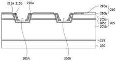
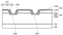
도 4a는 본 발명 다른 실시 예의 발광 소자의 단면도이며, 도 4b는 도 4a의 B 영역의 확대도이다. 상기와 같은 본 발명 다른 실시 예의 발광 소자는 도 1a 및 도 1b에 도시된 본 발명 실시 예와 제 1 전극, 제 2 전극 및 절연 패턴의 구조만이 상이하다.4A is a cross-sectional view of a light emitting device of another embodiment of the present invention, and FIG. 4B is an enlarged view of a region B of FIG. 4A. The light emitting device of another embodiment of the present invention differs from the embodiment of the present invention shown in FIGS. 1A and 1B only in the structure of the first electrode, the second electrode, and the insulation pattern.
도 4a 및 도 4b와 같이, 본 발명 다른 실시 예의 발광 소자는 콘택 전극(220a)이 접속 홈(205h) 내부에만 형성되고, 제 1 전극 패턴(210a)이 접속 홈(205h) 내부까지 연장되어, 제 1 전극 패턴(210a)과 콘택 전극(220a)이 접속 홈(205h) 내부에서 절연 패턴(215)을 사이에 두고 중첩된다.4A and 4B, the light emitting device according to another embodiment of the present invention has the
구체적으로, 반사층으로 기능하는 제 1 전극(210)의 제 1 전극 패턴(210a)은 제 1 반도체층(205a)과 접촉하도록 발광 구조물(205) 하부에 배치된다. 이 때, 제 1 전극 패턴(210a)의 끝단이 접속 홈(205h)의 내부까지 연장되어 제 1 전극 패턴(210a)과 활성층(205c)의 중첩 면적이 넓어진다. 이에 따라, 반사 효율이 향상되어 광 출력이 향상된다. 도면에서는 제 1 전극 패턴(210a)의 끝단이 접속 홈(205h)의 바닥면까지 연장된 것을 도시하였으나, 제 1 전극 패턴(210a)의 끝단은 접속 홈(205h)의 측면까지만 연장될 수도 있다.Specifically, the
제 1 전극 패턴(210a)을 감싸도록 제 1 전극 패턴(210a) 하부에 배치된 제 2 전극 패턴(210b)은 외부로부터 주입된 전류가 수평적으로 골고루 퍼질 수 있도록 우수한 전기 전도성을 갖는 물질로 형성될 수 있다. 도면에서는 제 2 전극 패턴(210b)이 접속 홈(205h) 내부에는 형성되지 않은 것을 도시하였으나, 제 2 전극 패턴(210b)은 제 1 전극 패턴(210a)과 같이 접속 홈(205h) 내부에도 형성될 수 있다.The
제 2 전극(220)은 접속 홈(205h) 내부에서 제 2 반도체층(205b)과 접촉하는 콘택 전극(220a)과 각 콘택 전극(220a)을 연결시키는 본딩 전극(220b)을 포함한다. 콘택 전극(220a)은 접속 홈(205h)의 바닥면 및 측면을 감싸도록 접속 홈(205h)의 가장자리까지 연장되어 접속 홈(205h) 내부에만 형성된다. 그리고, 본딩 전극(220b)은 콘택 전극(220a)과 전기적으로 연결되어 제 2 전극(220)의 하부면 전면에 형성된다.The
상기와 같은 제 1 전극(210)과 제 2 전극(220) 사이에는 절연 패턴(215)이 배치되어, 제 1 전극(210)과 제 2 전극(220)을 전기적으로 절연시킨다. 절연 패턴(215)은 제 1, 제 2 및 제 3 절연 패턴(215a, 215b 및 215c)을 포함할 수 있다.An
제 1 절연 패턴(215a)은 접속 홈(205h)의 측면에서 발광 구조물(205)과 콘택 전극(220a) 사이에 배치된다. 따라서, 콘택 전극(220a)과 활성층(205c) 및 콘택 전극(220a)과 제 1 반도체층(205a)은 제 1 절연 패턴(215a)을 통해 서로 절연될 수 있다. 그리고, 제 2 절연 패턴(215b)은 제 1 전극 패턴(210a)과 콘택 전극(220a) 사이에 배치된다. 따라서, 콘택 전극(220a)과 제 1 전극 패턴(210a)은 접속 홈(205h) 내부에서 제 2 절연 패턴(215b)을 사이에 두고 중첩될 수 있다. The
제 3 절연 패턴(215c)은 발광 구조물(205) 하부에서 본딩 전극(220b)과 제 1 전극(210) 사이에 배치된다. 따라서, 제 2 절연 패턴(215b)과 제 3 절연 패턴(215c)이 접속 홈(205h) 내부에서 콘택 전극(220a)을 노출시켜, 콘택 전극(220a)과 본딩 전극(220b)이 접속 홈(205h) 내부에서 전기적으로 연결될 수 있다.The third
상기와 같은 본 발명 다른 실시 예의 발광 소자는 제 1 반도체층(205a)과 접촉되는 제 1 전극(210)의 제 1 전극 패턴(210a)과 제 2 반도체층(205b)과 접촉되는 제 2 전극(220)의 콘택 전극(220a)이 접속 홈(205h) 내부에서 제 2 절연 패턴(215b)을 사이에 두고 서로 중첩된다. 따라서, 제 1 전극(210) 끝단과 제 2 전극(220) 끝단의 간격이 0(zero)으로, 발광 소자의 저항이 감소하여 구동 전압이 감소한다.The light emitting device according to another embodiment of the present invention includes the
이하, 첨부된 도면을 참조하여 본 발명 실시 예의 발광 소자의 제조 방법을 구체적으로 설명하면 다음과 같다.Hereinafter, a method of manufacturing a light emitting device according to an embodiment of the present invention will be described in detail with reference to the accompanying drawings.
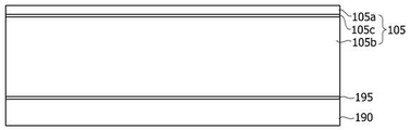
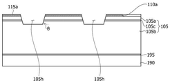
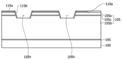
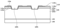
도 5a 내지 도 5i는 본 발명 실시 예의 발광 소자의 제조 방법을 나타낸 공정 단면도이다.5A to 5I are process cross-sectional views illustrating a method of manufacturing a light emitting device of an embodiment of the present invention.
도 5a와 같이, 베이스 기판(190) 상에 발광 구조물(105)을 형성한다. 발광 구조물(105)은 후술할 지지 기판을 절단할 때, 복수 개로 분리될 수 있다. 베이스 기판(190)은 사파이어(Al2O3), SiC, GaAs, GaN, ZnO, Si, GaP, InP 및 Ge 등에서 선택된 물질로 형성될 수 있으며, 이에 대해 한정하지는 않는다. 특히, 베이스 기판(190)은 후술할 지지 기판(125) 형성 시 발광 구조물(105)에서 분리되는 것으로, 베이스 기판(190)의 용이한 분리를 위해 베이스 기판(190)과 발광 구조물(105) 사이에 분리층(195)이 형성될 수 있다.As shown in FIG. 5A, a
구체적으로, 베이스 기판(190) 상에 유기금속 화학 증착법(Metal Organic Chemical Vapor Deposition; MOCVD), 화학 증착법(Chemical Vapor Deposition; CVD), 플라즈마 화학 증착법(Plasma-Enhanced Chemical Vapor Deposition; PECVD), 분자선 성장법(Molecular Beam Epitaxy; MBE), 수소화물 기상 성장법(Hydride Vapor Phase Epitaxy; HVPE), 스퍼터링(Sputtering) 등의 방법을 이용하여 발광 구조물(105)을 형성할 수 있으며, 이에 한정하지는 않는다. 발광 구조물(105)은 제 2 반도체층(105b), 활성층(105c) 및 제 1 반도체층(105a)이 차례로 적층된 구조이다. Specifically, a metal organic chemical vapor deposition (MOCVD), a chemical vapor deposition (CVD), a plasma enhanced chemical vapor deposition (PECVD), a molecular beam growth The
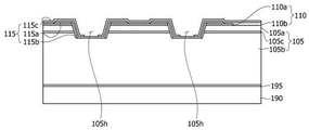
도 5b와 같이, 발광 구조물(105) 상에 제 1 전극 패턴(110a)과 제 1 절연 패턴(115a)을 차례로 형성하고, 접속 홈(105h)을 형성할 영역에서 제 1 전극 패턴(110a), 제 1 절연 패턴(115a) 및 발광 구조물(105)을 제거하여 제 2 반도체층(105b)의 일부를 노출시키는 접속 홈(105h)을 형성한다. 이에 따라, 제 1 전극 패턴(110a)의 끝단과 제 2 절연 패턴(115b)의 끝단이 접속 홈(105h)의 가장자리에서 일치한다.The
도면에서는 두 개의 접속 홈(105h)을 개시하였으나, 접속 홈(105h)의 개수는 이에 한정하지 않는다. 접속 홈(105h)은 제 2 반도체층(105b)을 노출시키는 바닥면과 제 1 반도체층(105a), 활성층(105c) 및 제 2 반도체층(105b)을 노출시키는 측면을 포함한다. 특히, 후술할 절연 물질층이 접속 홈(105h)의 측면에서 제거되는 것을 방지하기 위해, 접속 홈(105h)의 바닥면과 측면 사이의 경사각(θ)은 60°이상이며 90°이하일 수 있다.Although two
제 1 전극 패턴(110a)은 활성층(105c)에서 방출되는 광의 반사율을 향상시키기 위한 반사층으로 기능한다. 그리고, 제 1 절연 패턴(115a)은 제 1 전극 패턴(110a)과 후술할 콘택 전극(120a)을 절연시키기 위한 것이다.The
도 5c와 같이, 접속 홈(105h)의 측면에만 제 2 절연 패턴(115b)을 형성한다. 제 2 절연 패턴(115b)은 접속 홈(105h)을 덮도록 발광 구조물(105) 상부면 전면에 절연 물질층을 형성하고, 건식 식각(Dry Etch) 방법으로 절연 물질층을 제거하여 형성할 수 있다. 구체적으로, 발광 구조물(105)의 상부면과 수직인 방향에서 절연 물질층을 식각하면, 제 1 절연 패턴(115a)의 상부면 및 접속 홈(105h) 바닥면의 절연 물질층이 제거되어, 접속 홈(105h)의 측면에만 절연 물질층이 남게 되어 제 2 절연 패턴(115b)을 형성할 수 있다.As shown in FIG. 5C, the second
절연 물질층의 제거 시, 접속 홈(105h)의 바닥면과 측면 사이의 경사각(θ)이 60°미만인 경우, 접속 홈(105h)의 측면의 절연 물질층도 제거될 수 있다. 따라서, 상술한 바와 같이, 접속 홈(105h)의 바닥면과 측면 사이의 경사각(θ)은 60°이상이며 90°이하일 수 있다.When the inclination angle [theta] between the bottom surface and the side surface of the
도 5d와 같이, 접속 홈(105h)의 바닥면에서 노출된 제 2 반도체층(105b)과 접속하는 콘택 전극(120a)을 형성한다. 이 때, 콘택 전극(120a)은 제 1 절연 패턴(115a)을 사이에 두고 제 1 전극 패턴(110a)과 중첩되도록 제 1 절연 패턴(115a)의 상부면까지 연장된 구조이다.The
이어, 도 5e와 같이, 제 1 전극 패턴(110a) 상에 제 2 전극 패턴(110b)을 형성한다. 구체적으로, 제 2 전극 패턴(110b)을 형성하기 전에 제 2 전극 패턴(110b)을 형성할 영역의 제 1 절연 패턴(115a)을 제거한다. 또한, 후술할 전극 패드가 제 2 전극 패턴(110b)과 직접 접촉되도록, 전극 패드를 형성할 영역에서 제 1 전극 패턴(110a)을 더 제거하여 제 1 반도체층(105a)을 노출시킬 수 있다. 이 때, 제 1 절연 패턴(115a) 및 제 1 전극 패턴(110a)의 제거는 포토 리소그래피 공정으로 이루어질 수 있으며, 이에 한정하지 않는다.Next, as shown in FIG. 5E, a
그리고, 제 1 절연 패턴(115a)과 제 1 전극 패턴(110a)이 제거된 영역을 덮도록 제 1 반도체층(105a)의 전면에 제 2 전극 패턴(110b)을 형성한다. 제 2 전극 패턴(110b)은 외부로부터 주입된 전류가 수평적으로 골고루 퍼질 수 있도록 우수한 전기 전도성을 갖는 물질로 형성될 수 있다. 특히, 도면에서는 제 2 전극 패턴(110b)이 단일 층인 것을 도시하였으나, 제 2 전극 패턴(110b)은 투명 전도성 산화막과 불투명 금속이 혼합된 하나 또는 복수 개의 층으로 형성될 수 있으며, 이에 한정하지 않는다. 상기와 같은 제 1 전극 패턴(110a)과 제 2 전극 패턴(110b)은 제 1 반도체층(105a)과 전기적으로 연결되어 제 1 전극(110)으로 기능한다.A
도 5f와 같이, 콘택 전극(120a) 및 제 2 전극 패턴(110b)을 덮도록 발광 구조물(105) 상부면의 전면에 제 3 절연 패턴(115c)을 형성하고, 접속 홈(105h) 바닥면의 콘택 전극(120a)의 일부를 노출시키도록 제 3 절연 패턴(115c)을 선택적으로 제거한다. 따라서, 콘택 전극(120a)은 접속 홈(105h) 내부에서 일부가 노출된다.A third
이어, 도 5g와 같이, 노출된 콘택 전극(120a)과 전기적으로 연결되는 본딩 전극(120b)을 형성한다. 본딩 전극(120b)은 복수 개의 콘택 전극(120a)을 연결시킨다. 도면에서는 본딩 전극(120b)이 단일 층인 것을 도시하였으나, 본딩 전극(120b)은 투명 전도성 산화막과 불투명 금속이 혼합된 하나 또는 복수 개의 층으로 형성될 수 있으며, 이에 한정하지 않는다. 상기와 같은 콘택 전극(120a)과 본딩 전극(120b)은 제 2 반도체층(105b)과 전기적으로 연결되어 제 2 전극(120)으로 기능한다. 그리고, 제 3 절연 패턴(115c)에 의해 본딩 전극(120b)과 제 2 전극(120)이 절연된다.Next, as shown in FIG. 5G, a
그리고, 도 5h와 같이, 본딩 전극(120b)과 전기적으로 접속하는 지지 기판(125)을 형성한다. 지지 기판(125)은 본딩 방식, 도금 방식 또는 증착 방식으로 형성할 수 있다. 그리고, 발광 구조물(105)에 부착된 베이스 기판(190)을 제거한다. 베이스 기판(190)은 레이저 리프트 오프 방법을 이용하여 발광 구조물(105)에서 제거할 수 있다. 레이저 리프트 오프 방법은 베이스 기판(190)에 엑시머 레이저를 조사하여 실시할 수 있다. 레이저에 의해 베이스 기판(190)과 발광 구조물(105)의 경계면에 열 에너지가 집중되어 베이스 기판(190)이 분리층(195)에서 분리된다. 베이스 기판(190)을 분리한 후 남아있는 분리층(195)은 추가적인 식각 공정으로 제거할 수 있다.Then, as shown in Fig. 5H, a supporting
그리고, 발광 구조물(105)에 아이솔레이션(Isolation) 에칭을 더 실시할 수 있다. 아이솔레이션 에칭은 ICP(Inductively Coupled Plasma)와 같은 건식 식각 방법에 의해 실시될 수 있다. 아이솔레이션 에칭에 의해 제 2 전극 패턴(110b)의 일부가 발광 구조물(105) 외부로 개방될 수 있다. 그리고, 노출된 제 2 전극 패턴(110b)에 전극 패드(130)를 형성한다. 전극 패드(130)는 제 1 전극(110)과 전기적으로 연결된다.Further, the
이어, 도 5i와 같이, 제 2 반도체층(105b)의 상부면에 러프니스 패턴을 형성하고, 발광 구조물(105)을 감싸도록 보호층(135)을 더 형성할 수 있다.5I, a roughness pattern may be formed on the upper surface of the
이하, 본 발명 다른 실시 예의 발광 소자의 제조 방법을 설명하면 다음과 같다.Hereinafter, a method of manufacturing a light emitting device according to another embodiment of the present invention will be described.
도 6a 내지 도 6i는 본 발명 다른 실시 예의 발광 소자의 제조 방법을 나타낸 공정 단면도이다.6A to 6I are process sectional views showing a method for manufacturing a light emitting device according to another embodiment of the present invention.
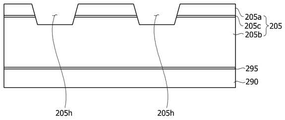
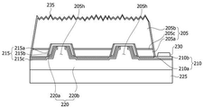
도 6a와 같이, 베이스 기판(290) 상에 발광 구조물(205)을 형성하고, 발광 구조물(205)을 선택적으로 제거하여 제 2 반도체층(205b)의 일부를 노출시키는 접속 홈(205h)을 형성한다. 발광 구조물(205)을 형성하는 방법은 상기 도 5a의 설명과 동일하다. 도면에서는 두 개의 접속 홈(205h)을 개시하였으나, 접속 홈(205h)의 개수는 이에 한정하지 않는다. 특히, 후술할 절연 물질층이 접속 홈(205h)의 측면에서 제거되는 것을 방지하기 위해, 접속 홈(205h)의 바닥면과 측면의 경사각(θ)은 60°이상이며 90°이하일 수 있다.6A, a
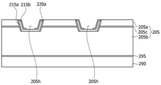
이어, 도 6b와 같이, 접속 홈(205h)의 측면에만 제 1 절연 패턴(215a)을 형성한다. 구체적으로, 접속 홈(205h)을 덮도록 발광 구조물(205) 상부면의 전면에 절연 물질층을 형성하고, 건식 식각(Dry Etch) 방법으로 발광 구조물(205)의 상부면과 수직인 방향에서 절연 물질층을 식각하여 제 1 반도체층(205a)의 상부면 및 접속 홈(205h)의 바닥면에 배치된 절연 물질층만 선택적으로 제거할 수 있다. 이에 따라, 접속 홈(205h)의 측면에만 절연 물질층이 남아, 제 1 절연 패턴(215a)이 형성된다.Next, as shown in FIG. 6B, the
도 6c와 같이, 접속 홈(205h)의 바닥면에 노출된 제 2 반도체층(205b) 상에 콘택 전극(220a)을 형성한다. 콘택 전극(220a)은 접속 홈(205h)의 바닥면과 측면을 감싸며 접속 홈(205h) 내부에만 형성된다. 즉, 콘택 전극(220a)은 접속 홈(205h)의 바닥면에서 노출된 제 2 반도체층(205b)과 직접 접촉하며, 접속 홈(205h)의 가장자리에서 제 1 절연 패턴(215a)의 일부를 노출시킨다. 이는, 후술할 제 2 전극과 콘택 전극(220a)이 접속 홈(205h)의 가장자리에서 접속되는 것을 방지하기 위함이다.The
도 6d와 같이, 콘택 전극(220a)을 덮도록 제 2 절연 패턴(215b)을 형성한다. 제 2 절연 패턴(215b)은 콘택 전극(220a)에 의해 노출된 제 1 절연 패턴(215a)과 접촉된다. 즉, 콘택 전극(220a)의 끝단은 제 1 절연 패턴(215a)과 제 2 절연 패턴(215b)에 의해 감싸진 구조이다.As shown in FIG. 6D, a second
도 6e와 같이, 접속 홈(205h) 바닥면의 제 2 절연 패턴(215b)의 일부를 노출시키도록 제 1 전극 패턴(210a)을 형성하고, 제 1 전극 패턴(210a) 상에 제 2 전극 패턴(210b)을 형성한다. 제 1 전극 패턴(210a)과 제 2 전극 패턴(210b)은 제 1 반도체층(205a)과 전기적으로 연결되어 제 1 전극(210)으로 기능한다.The
구체적으로, 제 1 전극 패턴(210a)의 끝단은 접속 홈(205h)의 내부까지 연장된 구조이다. 도면에서는 제 1 전극 패턴(210a)의 끝단이 접속 홈(205h)의 바닥면까지 연장된 것을 도시하였으나, 제 1 전극 패턴(210a)의 끝단은 접속 홈(205h)의 측면까지만 연장될 수도 있다. 또한, 도면에서는 제 2 전극 패턴(210b)이 접속 홈(205h) 내부에는 형성되지 않은 것을 도시하였으나, 제 2 전극 패턴(210b)의 끝단이 제 1 전극 패턴(210a)과 같이 접속 홈(205h) 내부까지 연장될 수 있다.Specifically, the end of the
그리고, 도 6f와 같이, 제 2 절연 패턴(215b) 및 제 1 전극(210)을 덮도록 발광 구조물(205) 전면에 제 3 절연 패턴(215c)을 형성하고, 접속 홈(205h) 바닥면의 콘택 전극(220a)의 일부를 노출시키도록 제 2 절연 패턴(215b)과 제 3 절연 패턴(215c)을 선택적으로 제거한다. 따라서, 콘택 전극(220a)이 접속 홈(205h) 내부에서 일부가 노출된다.6f, a
이어, 도 6g와 같이, 노출된 콘택 전극(220a)과 전기적으로 연결되는 본딩 전극(220b)을 형성한다. 본딩 전극(220b)은 복수 개의 콘택 전극(220a)을 연결시킨다. 본딩 전극(220b)은 콘택 전극(220a)과 전기적으로 연결되어 제 1 전극(210)의 상부면 전면에 형성될 수 있다. 상기와 같은 콘택 전극(220a)과 본딩 전극(220b)은 제 2 반도체층(205b)과 전기적으로 연결되어 제 2 전극(220)으로 기능한다.Next, as shown in FIG. 6G, a
그리고, 도 6h와 같이, 본딩 전극(220b) 상에 지지 기판(225)을 형성한다. 지지 기판(225)은 본딩 방식, 도금 방식 또는 증착 방식으로 형성할 수 있다. 그리고, 발광 구조물(205)에 부착된 베이스 기판(290)을 제거한다. 베이스 기판(290)은 레이저 리프트 오프 방법을 이용하여 발광 구조물(205)에서 제거할 수 있다. 레이저 리프트 오프 방법은 베이스 기판(290)에 엑시머 레이저를 조사하여 실시할 수 있다. 레이저에 의해 베이스 기판(290)과 발광 구조물(205)의 경계면에 열 에너지가 집중되어 베이스 기판(290)이 분리층(295)에서 분리된다. 베이스 기판(290)을 분리한 후 남아있는 분리층(295)은 추가적인 식각 공정으로 제거할 수 있다.6H, a supporting
그리고, 각 발광 구조물(205)에 아이솔레이션(Isolation) 에칭을 더 실시할 수 있다. 아이솔레이션 에칭은 ICP(Inductively Coupled Plasma)와 같은 건식 식각 방법에 의해 실시될 수 있다. 아이솔레이션 에칭에 의해 제 2 전극 패턴(210b)의 일부가 발광 구조물(205) 외부로 개방될 수 있다. 그리고, 노출된 제 2 전극 패턴(210b)에 전극 패드(230)를 형성한다. 전극 패드(230)는 제 1 전극(210)과 전기적으로 연결된다.Further, the
이어, 도 6i와 같이, 제 2 반도체층(205b)의 상부면에 러프니스 패턴을 형성하고, 발광 구조물(205)을 감싸도록 보호층(235)을 더 형성할 수 있다. 6I, a roughness pattern may be formed on the upper surface of the
상술한 바와 같이, 본 발명 실시 예의 발광 소자는 반사층으로 기능하는 제 1 전극 패턴(110a, 210a)과 활성층(105c, 205c)의 중첩 면적이 넓어져 반사 효율이 향상되어 광 출력이 향상된다. 또한, 제 2 반도체층(105b, 205b)과 직접 접촉되는 콘택 전극(120a, 220a)과 제 2 반도체층(105b, 205b)의 접촉 면적이 넓어져 구동 전압이 감소한다.As described above, in the light emitting device of the embodiment of the present invention, the overlapping area of the
그리고, 제 1 전극 패턴(110a, 210a)과 콘택 전극(120a, 220a)이 절연 패턴(115, 215)을 사이에 두고 중첩되어, 제 1 전극(110, 210) 끝단과 제 2 전극(120, 220) 끝단의 간격이 0(zero)이 되어 발광 소자의 저항이 감소하고 발광 소자의 구동 전압 역시 감소한다. 더욱이, 상기와 같은 본 발명 실시 예의 발광 소자를 반도체층의 저항이 높은 UV-B 및 UV-C 구조에 적용하는 경우, 구동 전압의 감소 및 광 효율 향상의 효과를 더욱 기대할 수 있다.The
도 7은 본 발명 실시 예의 발광 소자를 포함하는 발광 소자 패키지의 단면도이다.7 is a cross-sectional view of a light emitting device package including the light emitting device of the embodiment of the present invention.
도 7과 같이, 본 발명 실시 예의 발광 소자 패키지는 바디(15), 바디(15) 상에 형성된 발광 소자(100), 발광 소자(100)와 연결된 제 1 리드 프레임(20a)과 제 2 리드 프레임(20b) 및 발광 소자(100)를 감싸는 몰딩부(30)를 포함한다.7, the light emitting device package of the present invention includes a
바디(15)는 실리콘 재질, 합성수지 재질, 또는 금속 재질로 형성될 수 있으며, 이에 한정하지 않는다. 바디(15)가 금속과 같은 전도성 물질로 이루어지면, 바디(15) 표면에 절연 물질을 더 형성하여 제 1 리드 프레임(20a)과 제 2 리드 프레임(20b)의 전기적 연결을 방지할 수 있다.The
발광 소자(100)는 바디(15) 상에 설치되거나 제 1 리드 프레임(20a) 또는 제 2 리드 프레임(20b) 상에 설치될 수도 있다. 도면에서는 발광 소자(100)가 제 1 리드 프레임(20a)과 직접 연결되고, 발광 소자(100)가 제 2 리드 프레임(20b)과는 와이어(25)를 통해 연결된 것을 도시하였다. 본 발명 실시 예의 발광 소자(100)는 제 1 리드 프레임(20a)과 지지 기판(300)이 전기적으로 연결되고, 전극 패드(400)가 제 2 리드 프레임(20b)과 전기적으로 연결될 수 있다. 그리고, 몰딩부(30)는 발광 소자(100)를 덮는다. 도시하지는 않았으나, 몰딩부(30)는 형광체를 더 포함하여 이루어질 수 있다.The
실시 예의 발광 소자 패키지는 도광판, 프리즘 시트, 확산 시트 등의 광학 부재를 더 포함하여 이루어져 백라이트 유닛으로 기능할 수 있다. 또한, 실시 예의 발광 소자는 표시 장치, 조명 장치, 지시 장치에 더 적용될 수 있다.The light emitting device package of the embodiment further includes optical members such as a light guide plate, a prism sheet, and a diffusion sheet, and can function as a backlight unit. Further, the light emitting element of the embodiment can be further applied to a display device, a lighting device, and a pointing device.
이 때, 표시 장치는 바텀 커버, 반사판, 발광 모듈, 도광판, 광학 시트, 디스플레이 패널, 화상 신호 출력 회로 및 컬러 필터를 포함할 수 있다. 바텀 커버, 반사판, 발광 모듈, 도광판 및 광학 시트는 백라이트 유닛(Backlight Unit)을 이룰 수 있다.At this time, the display device may include a bottom cover, a reflector, a light emitting module, a light guide plate, an optical sheet, a display panel, an image signal output circuit, and a color filter. The bottom cover, the reflector, the light emitting module, the light guide plate, and the optical sheet may form a backlight unit.
반사판은 바텀 커버 상에 배치되고, 발광 모듈은 광을 방출한다. 도광판은 반사판의 전방에 배치되어 발광 모듈에서 발산되는 빛을 전방으로 안내하고, 광학 시트는 프리즘 시트 등을 포함하여 이루어져 도광판의 전방에 배치된다. 디스플레이 패널은 광학 시트 전방에 배치되고, 화상 신호 출력 회로는 디스플레이 패널에 화상 신호를 공급하며, 컬러 필터는 디스플레이 패널의 전방에 배치된다. The reflector is disposed on the bottom cover, and the light emitting module emits light. The light guide plate is disposed in front of the reflection plate to guide light emitted from the light emitting module forward, and the optical sheet includes a prism sheet or the like and is disposed in front of the light guide plate. The display panel is disposed in front of the optical sheet, and the image signal output circuit supplies an image signal to the display panel, and the color filter is disposed in front of the display panel.
그리고, 조명 장치는 기판과 실시 예의 발광 소자를 포함하는 광원 모듈, 광원 모듈의 열을 발산시키는 방열부 및 외부로부터 제공받은 전기적 신호를 처리 또는 변환하여 광원 모듈로 제공하는 전원 제공부를 포함할 수 있다. 더욱이 조명 장치는, 램프, 해드 램프, 또는 가로등 등을 포함할 수 있다.The lighting device may include a light source module including a substrate and a light emitting device of the embodiment, a heat dissipation unit that dissipates heat of the light source module, and a power supply unit that processes or converts an electric signal provided from the outside and provides the light source module . Further, the lighting device may include a lamp, a head lamp, or a street lamp or the like.
이상에서 설명한 본 발명 실시 예는 상술한 실시 예 및 첨부된 도면에 한정되는 것이 아니고, 실시 예의 기술적 사상을 벗어나지 않는 범위 내에서 여러 가지 치환, 변형 및 변경이 가능하다는 것이 본 발명 실시 예가 속하는 기술분야에서 종래의 지식을 가진 자에게 있어 명백할 것이다.It will be apparent to those skilled in the art that various changes, substitutions, and alterations can be made hereto without departing from the spirit and scope of the invention as defined in the appended claims. Will be apparent to those of ordinary skill in the art.
15: 바디
20a: 제 1 리드 프레임
20b: 제 2 리드 프레임
25: 와이어
30: 몰딩부
100: 발광 소자
105, 205: 발광 구조물
105a, 205a: 제 1 반도체층
105b, 205b: 제 2 반도체층
105c, 205c: 활성층
105h, 205h: 접속 홈
110, 210: 제 1 전극
110a, 210a: 제 1 전극 패턴
110b, 210b: 제 2 전극 패턴
115, 215: 절연 패턴
115a, 215a: 제 1 절연 패턴
115b, 215b: 제 2 절연 패턴
115c, 215c: 제 3 절연 패턴
120, 220: 제 2 전극
120a, 220a: 콘택 전극
120b, 220b: 본딩 전극
125, 225: 지지 기판
130, 230: 전극 패드
135, 235: 보호층
190, 290: 베이스 기판
195, 295: 분리층15:
20b: second lead frame 25: wire
30: molding part 100: light emitting element
105, and 205: light emitting
105b and 205b: second semiconductor layers 105c and 205c:
105h, 205h:
110a, 210a:
115, 215:
115b, 215b:
120, 220:
120b, 220b:
130, 230:
190, 290:
Claims (20)
상기 지지 기판 상에 배치되며, 제 1 반도체층, 활성층 및 제 2 반도체층을 포함하는 발광 구조물;
상기 발광 구조물이 제거되어 상기 제 2 반도체층을 노출시키는 바닥면과 상기 제 1 반도체층, 활성층 및 제 2 반도체층을 노출시키는 측면을 포함하는 복수 개의 접속 홈;
상기 제 1 반도체층과 접촉하도록 상기 발광 구조물 상에 배치되며, 끝단이 상기 접속 홈의 가장자리까지 연장된 제 1 전극 패턴 및 상기 제 1 전극 패턴 상에 배치된 제 2 전극 패턴을 포함하는 제 1 전극;
상기 접속 홈의 바닥면 및 측면을 감싸도록 상기 제 1 반도체층의 상부면까지 연장된 콘택 전극 및 복수 개의 상기 콘택 전극과 연결된 본딩 전극을 포함하는 제 2 전극; 및
상기 제 1 전극과 상기 제 2 전극 사이에 배치된 절연 패턴을 포함하는 발광 소자.A support substrate;
A light emitting structure disposed on the supporting substrate, the light emitting structure including a first semiconductor layer, an active layer, and a second semiconductor layer;
A plurality of connection grooves including a bottom surface from which the light emitting structure is removed to expose the second semiconductor layer and a side surface that exposes the first semiconductor layer, the active layer, and the second semiconductor layer;
A first electrode pattern disposed on the light emitting structure so as to be in contact with the first semiconductor layer, the first electrode pattern having an end extending to an edge of the connection groove, and a second electrode pattern disposed on the first electrode pattern; ;
A second electrode including a contact electrode extending to an upper surface of the first semiconductor layer so as to surround a bottom surface and a side surface of the connection groove, and a bonding electrode connected to the plurality of contact electrodes; And
And an insulating pattern disposed between the first electrode and the second electrode.
상기 절연 패턴은 상기 제 1 반도체층 상에서 상기 콘택 전극과 상기 제 1 전극 패턴 사이에 배치된 제 1 절연 패턴;
상기 접속 홈의 측면에서 상기 콘택 전극과 상기 제 1 전극 패턴 사이에 배치된 제 2 절연 패턴; 및
상기 발광 구조물 상에서 상기 본딩 전극과 상기 제 2 전극 패턴 사이에 배치된 제 3 절연 패턴을 포함하는 발광 소자.The method according to claim 1,
Wherein the insulating pattern is a first insulating pattern disposed between the contact electrode and the first electrode pattern on the first semiconductor layer;
A second insulation pattern disposed between the contact electrode and the first electrode pattern on a side surface of the connection groove; And
And a third insulation pattern disposed between the bonding electrode and the second electrode pattern on the light emitting structure.
상기 콘택 전극과 상기 제 1 전극 패턴은 상기 제 1 반도체층 상에서 상기 제 1 절연 패턴을 사이에 두고 중첩되는 발광 소자. 3. The method of claim 2,
Wherein the contact electrode and the first electrode pattern are overlapped on the first semiconductor layer with the first insulation pattern interposed therebetween.
상기 접속 홈의 가장자리에서 상기 제 1 전극 패턴과 상기 제 1 절연 패턴이 상기 제 2 절연 패턴과 접촉하는 발광 소자.3. The method of claim 2,
And the first electrode pattern and the first insulation pattern are in contact with the second insulation pattern at the edge of the connection groove.
상기 콘택 전극과 상기 제 1 전극 패턴, 상기 콘택 전극과 상기 활성층 및 상기 콘택 전극과 상기 제 1 반도체층은 상기 제 2 절연 패턴을 통해 서로 절연된 발광 소자.3. The method of claim 2,
Wherein the contact electrode, the first electrode pattern, the contact electrode, the active layer, the contact electrode, and the first semiconductor layer are insulated from each other through the second insulation pattern.
상기 제 3 절연 패턴이 상기 접속 홈 내부의 상기 콘택 전극을 노출시켜, 상기 콘택 전극과 상기 본딩 전극이 상기 접속 홈 내부에서 전기적으로 연결된 발광 소자.3. The method of claim 2,
The third insulation pattern exposes the contact electrode in the connection groove, and the contact electrode and the bonding electrode are electrically connected in the connection groove.
상기 제 3 절연 패턴은 상기 접속 홈 내부의 상기 콘택 전극을 노출시키며 상기 제 1 전극의 하부면 전면에 배치된 발광 소자.3. The method of claim 2,
Wherein the third insulating pattern exposes the contact electrode in the connection groove and is disposed on the entire lower surface of the first electrode.
상기 접속 홈의 상기 측면과 상기 바닥면 사이의 경사각이 60°이상이며 90°이하인 발광 소자.The method according to claim 1,
Wherein an inclination angle between the side surface of the connection groove and the bottom surface is 60 degrees or more and 90 degrees or less.
상기 제 1 전극 패턴은 상기 활성층에서 발생한 광을 상기 제 2 반도체층으로 반사시키는 반사층인 발광 소자.The method according to claim 1,
Wherein the first electrode pattern is a reflective layer that reflects light generated in the active layer to the second semiconductor layer.
상기 지지 기판은 상기 제 2 전극과 전기적으로 연결된 발광 소자.The method according to claim 1,
And the supporting substrate is electrically connected to the second electrode.
상기 지지 기판 상에 배치되며, 제 1 반도체층, 활성층 및 제 2 반도체층을 포함하는 발광 구조물;
상기 발광 구조물이 제거되어 상기 제 2 반도체층을 노출시키는 바닥면과 상기 제 1 반도체층, 활성층 및 제 2 반도체층을 노출시키는 측면을 포함하는 복수 개의 접속 홈;
상기 제 1 반도체층과 전기적으로 연결되며, 상기 접속 홈의 내부까지 연장된 제 1 전극 패턴 및 상기 제 1 전극 패턴 상에 배치된 제 2 전극 패턴을 포함하는 제 1 전극;
상기 접속 홈의 바닥면 및 측면을 감싸도록 상기 접속 홈의 가장자리까지 연장된 콘택 전극 및 복수 개의 상기 콘택 전극과 연결된 본딩 전극을 포함하는 제 2 전극; 및
상기 제 1 전극과 상기 제 2 전극 사이에 배치된 절연 패턴을 포함하는 발광 소자.A support substrate;
A light emitting structure disposed on the supporting substrate, the light emitting structure including a first semiconductor layer, an active layer, and a second semiconductor layer;
A plurality of connection grooves including a bottom surface from which the light emitting structure is removed to expose the second semiconductor layer and a side surface that exposes the first semiconductor layer, the active layer, and the second semiconductor layer;
A first electrode electrically connected to the first semiconductor layer, the first electrode including a first electrode pattern extended to the inside of the connection groove and a second electrode pattern disposed on the first electrode pattern;
A second electrode including a contact electrode extending to an edge of the connection groove and a bonding electrode connected to the plurality of contact electrodes so as to surround the bottom surface and the side surface of the connection groove; And
And an insulating pattern disposed between the first electrode and the second electrode.
상기 제 1 전극 패턴과 상기 콘택 전극은 상기 접속 홈 내부에서 상기 절연 패턴을 사이에 두고 서로 중첩되는 발광 소자.12. The method of claim 11,
Wherein the first electrode pattern and the contact electrode overlap each other with the insulating pattern interposed in the connection groove.
상기 절연 패턴은 상기 접속 홈의 측면에서 상기 발광 구조물과 상기 콘택 전극 사이에 배치된 제 1 절연 패턴;
상기 제 1 전극 패턴과 상기 콘택 전극 사이에 배치된 제 2 절연 패턴; 및
상기 발광 구조물 상에서 상기 본딩 전극과 상기 제 1 전극 사이에 배치된 제 3 절연 패턴을 포함하는 발광 소자.12. The method of claim 11,
Wherein the insulating pattern is a first insulating pattern disposed between the light emitting structure and the contact electrode at a side surface of the connection groove;
A second insulation pattern disposed between the first electrode pattern and the contact electrode; And
And a third insulating pattern disposed between the bonding electrode and the first electrode on the light emitting structure.
상기 콘택 전극과 상기 활성층 및 상기 콘택 전극과 상기 제 1 반도체층은 상기 제 1 절연 패턴을 통해 서로 절연된 발광 소자.14. The method of claim 13,
Wherein the contact electrode, the active layer, the contact electrode, and the first semiconductor layer are insulated from each other through the first insulating pattern.
상기 콘택 전극의 끝단은 상기 접속 홈의 가장자리에서 상기 제 1 절연 패턴과 상기 제 2 절연 패턴에 의해 감싸진 발광 소자.14. The method of claim 13,
And an end of the contact electrode is surrounded by the first insulation pattern and the second insulation pattern at an edge of the connection groove.
상기 제 2 절연 패턴과 제 3 절연 패턴이 상기 접속 홈의 바닥면에서 상기 콘택 전극을 노출시켜, 상기 콘택 전극과 상기 본딩 전극이 상기 접속 홈 내부에서 전기적으로 연결된 발광 소자.14. The method of claim 13,
The second insulation pattern and the third insulation pattern expose the contact electrode on the bottom surface of the connection groove, and the contact electrode and the bonding electrode are electrically connected in the connection groove.
상기 제 3 절연 패턴은 상기 접속 홈 내부의 상기 콘택 전극을 노출시키며 상기 제 1 전극의 하부면 전면에 배치된 발광 소자.14. The method of claim 13,
Wherein the third insulating pattern exposes the contact electrode in the connection groove and is disposed on the entire lower surface of the first electrode.
상기 접속 홈의 상기 측면과 상기 바닥면 사이의 경사각이 60°이상이며 90°이하인 발광 소자.12. The method of claim 11,
Wherein an inclination angle between the side surface of the connection groove and the bottom surface is 60 degrees or more and 90 degrees or less.
상기 제 1 전극 패턴은 상기 활성층에서 발생한 광을 상기 제 2 반도체층으로 반사시키는 반사층인 발광 소자.12. The method of claim 11,
Wherein the first electrode pattern is a reflective layer that reflects light generated in the active layer to the second semiconductor layer.
상기 지지 기판은 상기 제 2 전극과 전기적으로 연결된 발광 소자.12. The method of claim 11,
And the supporting substrate is electrically connected to the second electrode.
Priority Applications (4)
| Application Number | Priority Date | Filing Date | Title |
|---|---|---|---|
| KR1020150069775A KR102371326B1 (en) | 2015-05-19 | 2015-05-19 | Light emitting device |
| CN201680029225.7A CN107636846B (en) | 2015-05-19 | 2016-04-22 | Light emitting element |
| PCT/KR2016/004245 WO2016186330A1 (en) | 2015-05-19 | 2016-04-22 | Light-emitting element |
| US15/575,242 US10333029B2 (en) | 2015-05-19 | 2016-04-22 | Light-emitting element |
Applications Claiming Priority (1)
| Application Number | Priority Date | Filing Date | Title |
|---|---|---|---|
| KR1020150069775A KR102371326B1 (en) | 2015-05-19 | 2015-05-19 | Light emitting device |
Publications (2)
| Publication Number | Publication Date |
|---|---|
| KR20160136070A true KR20160136070A (en) | 2016-11-29 |
| KR102371326B1 KR102371326B1 (en) | 2022-03-07 |
Family
ID=57320412
Family Applications (1)
| Application Number | Title | Priority Date | Filing Date |
|---|---|---|---|
| KR1020150069775A Expired - Fee Related KR102371326B1 (en) | 2015-05-19 | 2015-05-19 | Light emitting device |
Country Status (4)
| Country | Link |
|---|---|
| US (1) | US10333029B2 (en) |
| KR (1) | KR102371326B1 (en) |
| CN (1) | CN107636846B (en) |
| WO (1) | WO2016186330A1 (en) |
Families Citing this family (4)
| Publication number | Priority date | Publication date | Assignee | Title |
|---|---|---|---|---|
| DE102018124341B4 (en) * | 2018-10-02 | 2024-05-29 | OSRAM Opto Semiconductors Gesellschaft mit beschränkter Haftung | Device with enlarged active zone and method for manufacturing |
| CN112038883B (en) * | 2020-10-29 | 2021-05-28 | 锐驰智光(北京)科技有限公司 | Laser transmitter module and lidar with the same |
| CN112711008B (en) * | 2021-03-26 | 2021-06-25 | 锐驰智光(北京)科技有限公司 | Laser emission module and laser radar with same |
| US20250228042A1 (en) * | 2024-01-08 | 2025-07-10 | Lumileds Llc | Light emitting devices having aluminum indium gallium phosphide die with embedded contacts |
Citations (6)
| Publication number | Priority date | Publication date | Assignee | Title |
|---|---|---|---|---|
| KR20110102630A (en) * | 2010-03-11 | 2011-09-19 | 삼성엘이디 주식회사 | Nitride semiconductor light emitting device and manufacturing method |
| KR20110136111A (en) * | 2010-06-14 | 2011-12-21 | 서울옵토디바이스주식회사 | Light emitting device and method of manufacturing the same |
| JP2013201411A (en) * | 2012-02-24 | 2013-10-03 | Stanley Electric Co Ltd | Semiconductor light-emitting device |
| US20140209952A1 (en) * | 2010-03-31 | 2014-07-31 | Seoul Viosys Co., Ltd. | High efficiency light emitting diode and method for fabricating the same |
| KR20140102509A (en) * | 2013-02-14 | 2014-08-22 | 엘지이노텍 주식회사 | Light emitting device, light emitting device package, and light unit |
| WO2014195420A1 (en) * | 2013-06-06 | 2014-12-11 | Osram Opto Semiconductors Gmbh | Light-emitting diode with passivation layer |
Family Cites Families (3)
| Publication number | Priority date | Publication date | Assignee | Title |
|---|---|---|---|---|
| JP3322300B2 (en) * | 1997-11-14 | 2002-09-09 | 日亜化学工業株式会社 | Gallium nitride based semiconductor light emitting device and light receiving device |
| JP6023660B2 (en) | 2013-05-30 | 2016-11-09 | スタンレー電気株式会社 | Semiconductor light emitting device and semiconductor light emitting device |
| KR20160149363A (en) * | 2015-06-17 | 2016-12-28 | 삼성전자주식회사 | Semiconductor light emitting device |
-
2015
- 2015-05-19 KR KR1020150069775A patent/KR102371326B1/en not_active Expired - Fee Related
-
2016
- 2016-04-22 US US15/575,242 patent/US10333029B2/en active Active
- 2016-04-22 CN CN201680029225.7A patent/CN107636846B/en active Active
- 2016-04-22 WO PCT/KR2016/004245 patent/WO2016186330A1/en not_active Ceased
Patent Citations (6)
| Publication number | Priority date | Publication date | Assignee | Title |
|---|---|---|---|---|
| KR20110102630A (en) * | 2010-03-11 | 2011-09-19 | 삼성엘이디 주식회사 | Nitride semiconductor light emitting device and manufacturing method |
| US20140209952A1 (en) * | 2010-03-31 | 2014-07-31 | Seoul Viosys Co., Ltd. | High efficiency light emitting diode and method for fabricating the same |
| KR20110136111A (en) * | 2010-06-14 | 2011-12-21 | 서울옵토디바이스주식회사 | Light emitting device and method of manufacturing the same |
| JP2013201411A (en) * | 2012-02-24 | 2013-10-03 | Stanley Electric Co Ltd | Semiconductor light-emitting device |
| KR20140102509A (en) * | 2013-02-14 | 2014-08-22 | 엘지이노텍 주식회사 | Light emitting device, light emitting device package, and light unit |
| WO2014195420A1 (en) * | 2013-06-06 | 2014-12-11 | Osram Opto Semiconductors Gmbh | Light-emitting diode with passivation layer |
Also Published As
| Publication number | Publication date |
|---|---|
| KR102371326B1 (en) | 2022-03-07 |
| CN107636846A (en) | 2018-01-26 |
| CN107636846B (en) | 2020-06-16 |
| WO2016186330A1 (en) | 2016-11-24 |
| US10333029B2 (en) | 2019-06-25 |
| US20180138366A1 (en) | 2018-05-17 |
Similar Documents
| Publication | Publication Date | Title |
|---|---|---|
| US10411166B2 (en) | Light emitting device and lighting apparatus | |
| US8450762B2 (en) | Light emitting device | |
| US7919784B2 (en) | Semiconductor light-emitting device and method for making same | |
| KR101752663B1 (en) | Light emitting device and method for manufacturing light emitting device | |
| KR101014071B1 (en) | Light emitting device, light emitting device manufacturing method, light emitting device package and lighting system | |
| US20110084306A1 (en) | Semiconductor light emitting device | |
| KR101034144B1 (en) | Light emitting device, light emitting device manufacturing method, light emitting device package and lighting system | |
| JP2011519161A (en) | Semiconductor light emitting device | |
| KR101769048B1 (en) | Light emitting device, light emitting device package and lighting installation having the same | |
| KR101803569B1 (en) | Light emitting device | |
| KR20170083353A (en) | Light emitting device | |
| US10333029B2 (en) | Light-emitting element | |
| CN108431970B (en) | Light emitting element | |
| US9741903B2 (en) | Light-emitting device and light emitting device package having the same | |
| KR102371327B1 (en) | Light emitting device | |
| KR101826979B1 (en) | Light emitting device and light emitting device package | |
| KR20170095675A (en) | Light emitting device | |
| US10236417B2 (en) | Light-emitting element | |
| KR101776302B1 (en) | Light emitting device and light emitting device package | |
| KR102234117B1 (en) | Light emitting device and lighting system | |
| KR20120037100A (en) | A light emitting device and a light emitting device package | |
| KR101710889B1 (en) | Light Emitting Device | |
| KR20170105996A (en) | Light emitting device | |
| KR101786081B1 (en) | Light emitting device and light emitting device package | |
| KR20110118380A (en) | Light emitting device, light emitting device manufacturing method, light emitting device package, lighting system |
Legal Events
| Date | Code | Title | Description |
|---|---|---|---|
| PA0109 | Patent application |
St.27 status event code: A-0-1-A10-A12-nap-PA0109 |
|
| PG1501 | Laying open of application |
St.27 status event code: A-1-1-Q10-Q12-nap-PG1501 |
|
| R18-X000 | Changes to party contact information recorded |
St.27 status event code: A-3-3-R10-R18-oth-X000 |
|
| R18-X000 | Changes to party contact information recorded |
St.27 status event code: A-3-3-R10-R18-oth-X000 |
|
| P22-X000 | Classification modified |
St.27 status event code: A-2-2-P10-P22-nap-X000 |
|
| R18-X000 | Changes to party contact information recorded |
St.27 status event code: A-3-3-R10-R18-oth-X000 |
|
| A201 | Request for examination | ||
| PA0201 | Request for examination |
St.27 status event code: A-1-2-D10-D11-exm-PA0201 |
|
| PN2301 | Change of applicant |
St.27 status event code: A-3-3-R10-R13-asn-PN2301 St.27 status event code: A-3-3-R10-R11-asn-PN2301 |
|
| N231 | Notification of change of applicant | ||
| PN2301 | Change of applicant |
St.27 status event code: A-3-3-R10-R13-asn-PN2301 St.27 status event code: A-3-3-R10-R11-asn-PN2301 |
|
| E902 | Notification of reason for refusal | ||
| PE0902 | Notice of grounds for rejection |
St.27 status event code: A-1-2-D10-D21-exm-PE0902 |
|
| E13-X000 | Pre-grant limitation requested |
St.27 status event code: A-2-3-E10-E13-lim-X000 |
|
| P11-X000 | Amendment of application requested |
St.27 status event code: A-2-2-P10-P11-nap-X000 |
|
| P13-X000 | Application amended |
St.27 status event code: A-2-2-P10-P13-nap-X000 |
|
| E701 | Decision to grant or registration of patent right | ||
| PE0701 | Decision of registration |
St.27 status event code: A-1-2-D10-D22-exm-PE0701 |
|
| GRNT | Written decision to grant | ||
| PR0701 | Registration of establishment |
St.27 status event code: A-2-4-F10-F11-exm-PR0701 |
|
| PR1002 | Payment of registration fee |
St.27 status event code: A-2-2-U10-U11-oth-PR1002 Fee payment year number: 1 |
|
| PG1601 | Publication of registration |
St.27 status event code: A-4-4-Q10-Q13-nap-PG1601 |
|
| P22-X000 | Classification modified |
St.27 status event code: A-4-4-P10-P22-nap-X000 |
|
| PC1903 | Unpaid annual fee |
St.27 status event code: A-4-4-U10-U13-oth-PC1903 Not in force date: 20250303 Payment event data comment text: Termination Category : DEFAULT_OF_REGISTRATION_FEE |
|
| H13 | Ip right lapsed |
Free format text: ST27 STATUS EVENT CODE: N-4-6-H10-H13-OTH-PC1903 (AS PROVIDED BY THE NATIONAL OFFICE); TERMINATION CATEGORY : DEFAULT_OF_REGISTRATION_FEE Effective date: 20250303 |
|
| PC1903 | Unpaid annual fee |
St.27 status event code: N-4-6-H10-H13-oth-PC1903 Ip right cessation event data comment text: Termination Category : DEFAULT_OF_REGISTRATION_FEE Not in force date: 20250303 |