KR20170004123A - 센서 소자 및 그 제조 방법 - Google Patents
센서 소자 및 그 제조 방법 Download PDFInfo
- Publication number
- KR20170004123A KR20170004123A KR1020150094036A KR20150094036A KR20170004123A KR 20170004123 A KR20170004123 A KR 20170004123A KR 1020150094036 A KR1020150094036 A KR 1020150094036A KR 20150094036 A KR20150094036 A KR 20150094036A KR 20170004123 A KR20170004123 A KR 20170004123A
- Authority
- KR
- South Korea
- Prior art keywords
- frame
- die
- trench
- sensor element
- present
- Prior art date
- Legal status (The legal status is an assumption and is not a legal conclusion. Google has not performed a legal analysis and makes no representation as to the accuracy of the status listed.)
- Ceased
Links
Images


Classifications
-
- G—PHYSICS
- G01—MEASURING; TESTING
- G01L—MEASURING FORCE, STRESS, TORQUE, WORK, MECHANICAL POWER, MECHANICAL EFFICIENCY, OR FLUID PRESSURE
- G01L13/00—Devices or apparatus for measuring differences of two or more fluid pressure values
- G01L13/06—Devices or apparatus for measuring differences of two or more fluid pressure values using electric or magnetic pressure-sensitive elements
-
- B—PERFORMING OPERATIONS; TRANSPORTING
- B81—MICROSTRUCTURAL TECHNOLOGY
- B81B—MICROSTRUCTURAL DEVICES OR SYSTEMS, e.g. MICROMECHANICAL DEVICES
- B81B7/00—Microstructural systems; Auxiliary parts of microstructural devices or systems
- B81B7/0032—Packages or encapsulation
- B81B7/0045—Packages or encapsulation for reducing stress inside of the package structure
- B81B7/0048—Packages or encapsulation for reducing stress inside of the package structure between the MEMS die and the substrate
-
- B—PERFORMING OPERATIONS; TRANSPORTING
- B81—MICROSTRUCTURAL TECHNOLOGY
- B81B—MICROSTRUCTURAL DEVICES OR SYSTEMS, e.g. MICROMECHANICAL DEVICES
- B81B3/00—Devices comprising flexible or deformable elements, e.g. comprising elastic tongues or membranes
- B81B3/0064—Constitution or structural means for improving or controlling the physical properties of a device
- B81B3/0067—Mechanical properties
- B81B3/0072—For controlling internal stress or strain in moving or flexible elements, e.g. stress compensating layers
-
- B—PERFORMING OPERATIONS; TRANSPORTING
- B81—MICROSTRUCTURAL TECHNOLOGY
- B81B—MICROSTRUCTURAL DEVICES OR SYSTEMS, e.g. MICROMECHANICAL DEVICES
- B81B7/00—Microstructural systems; Auxiliary parts of microstructural devices or systems
- B81B7/0009—Structural features, others than packages, for protecting a device against environmental influences
- B81B7/0029—Protection against environmental influences not provided for in groups B81B7/0012 - B81B7/0025
-
- B—PERFORMING OPERATIONS; TRANSPORTING
- B81—MICROSTRUCTURAL TECHNOLOGY
- B81C—PROCESSES OR APPARATUS SPECIALLY ADAPTED FOR THE MANUFACTURE OR TREATMENT OF MICROSTRUCTURAL DEVICES OR SYSTEMS
- B81C1/00—Manufacture or treatment of devices or systems in or on a substrate
- B81C1/00388—Etch mask forming
- B81C1/00404—Mask characterised by its size, orientation or shape
-
- G—PHYSICS
- G01—MEASURING; TESTING
- G01P—MEASURING LINEAR OR ANGULAR SPEED, ACCELERATION, DECELERATION, OR SHOCK; INDICATING PRESENCE, ABSENCE, OR DIRECTION, OF MOVEMENT
- G01P15/00—Measuring acceleration; Measuring deceleration; Measuring shock, i.e. sudden change of acceleration
- G01P15/02—Measuring acceleration; Measuring deceleration; Measuring shock, i.e. sudden change of acceleration by making use of inertia forces using solid seismic masses
- G01P15/08—Measuring acceleration; Measuring deceleration; Measuring shock, i.e. sudden change of acceleration by making use of inertia forces using solid seismic masses with conversion into electric or magnetic values
- G01P15/09—Measuring acceleration; Measuring deceleration; Measuring shock, i.e. sudden change of acceleration by making use of inertia forces using solid seismic masses with conversion into electric or magnetic values by piezoelectric pick-up
-
- B—PERFORMING OPERATIONS; TRANSPORTING
- B81—MICROSTRUCTURAL TECHNOLOGY
- B81B—MICROSTRUCTURAL DEVICES OR SYSTEMS, e.g. MICROMECHANICAL DEVICES
- B81B2201/00—Specific applications of microelectromechanical systems
- B81B2201/02—Sensors
- B81B2201/0264—Pressure sensors
-
- B—PERFORMING OPERATIONS; TRANSPORTING
- B81—MICROSTRUCTURAL TECHNOLOGY
- B81B—MICROSTRUCTURAL DEVICES OR SYSTEMS, e.g. MICROMECHANICAL DEVICES
- B81B2203/00—Basic microelectromechanical structures
- B81B2203/01—Suspended structures, i.e. structures allowing a movement
- B81B2203/0109—Bridges
-
- B—PERFORMING OPERATIONS; TRANSPORTING
- B81—MICROSTRUCTURAL TECHNOLOGY
- B81B—MICROSTRUCTURAL DEVICES OR SYSTEMS, e.g. MICROMECHANICAL DEVICES
- B81B2203/00—Basic microelectromechanical structures
- B81B2203/01—Suspended structures, i.e. structures allowing a movement
- B81B2203/0118—Cantilevers
-
- B—PERFORMING OPERATIONS; TRANSPORTING
- B81—MICROSTRUCTURAL TECHNOLOGY
- B81B—MICROSTRUCTURAL DEVICES OR SYSTEMS, e.g. MICROMECHANICAL DEVICES
- B81B2203/00—Basic microelectromechanical structures
- B81B2203/03—Static structures
- B81B2203/0323—Grooves
- B81B2203/033—Trenches
-
- B—PERFORMING OPERATIONS; TRANSPORTING
- B81—MICROSTRUCTURAL TECHNOLOGY
- B81C—PROCESSES OR APPARATUS SPECIALLY ADAPTED FOR THE MANUFACTURE OR TREATMENT OF MICROSTRUCTURAL DEVICES OR SYSTEMS
- B81C2201/00—Manufacture or treatment of microstructural devices or systems
- B81C2201/01—Manufacture or treatment of microstructural devices or systems in or on a substrate
- B81C2201/0101—Shaping material; Structuring the bulk substrate or layers on the substrate; Film patterning
- B81C2201/0128—Processes for removing material
- B81C2201/013—Etching
- B81C2201/0132—Dry etching, i.e. plasma etching, barrel etching, reactive ion etching [RIE], sputter etching or ion milling
Landscapes
- Engineering & Computer Science (AREA)
- Microelectronics & Electronic Packaging (AREA)
- Computer Hardware Design (AREA)
- Mechanical Engineering (AREA)
- Health & Medical Sciences (AREA)
- General Health & Medical Sciences (AREA)
- Toxicology (AREA)
- Manufacturing & Machinery (AREA)
- Pressure Sensors (AREA)
- Physics & Mathematics (AREA)
- General Physics & Mathematics (AREA)
Abstract
Description
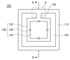
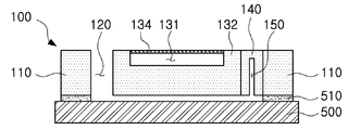
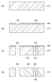
도 2는 도 1의 A부분을 확대하여 도시한 사시도이다.
도 3은 본 발명의 제1실시예에 따른 센서 소자를 도시한 도 1의 B-B선도이다.
도 4는 본 발명의 제1실시예에 따른 센서 소자가 변형된 상태를 도시한 도 1의 B-B선도이다.
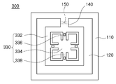
도 5는 본 발명의 제2실시예에 따른 센서 소자를 도시한 평면도이다.
도 6은 도 4의 C부분을 확대하여 도시한 사시도이다.
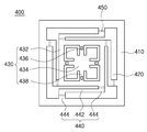
도 7은 본 발명의 제3실시예에 따른 센서 소자를 도시한 평면도이다.
도 8은 본 발명의 제4실시예에 따른 센서 소자를 도시한 평면도이다.
도 9는 본 발명에 따른 센서 소자의 제조 방법을 개략적으로 나타낸 도면들이다.
도 10은 마이크로로딩 효과를 설명하기 위한 도면이다.
110, 210, 410, 610: 다이
120, 220, 420, 620: 제1트렌치
130, 330, 430: 활성부
132, 332, 432, 632: 프레임
140: 브릿지
240, 440: 탄성 지지부
244, 444: 연결부
150, 250, 450, 650; 제2트렌치
660: 에치 마스크
Claims (14)
- 다이;
제1트렌치를 사이에 두고 상기 다이에 의해 포위된 프레임을 구비하는 활성부; 및
상기 다이와 상기 프레임을 연결하며, 제2트렌치가 형성되어 있는 적어도 하나의 브릿지
를 포함하는 센서 소자. - 제1항에 있어서,
상기 다이의 하단은 기판에 고정되고,
상기 프레임의 하단과 상기 기판 사이에는 공간이 형성되는 센서 소자. - 제1항에 있어서,
상기 활성부는,
상면에 캐비티가 형성된 상기 프레임;
상기 프레임의 상면에 형성되어 상기 캐비티를 덮어씌우는 멤브레인; 및
상기 멤브레인에 배치된 적어도 하나의 감지부
를 포함한 센서 소자. - 제1항에 있어서,
상기 활성부는,
캐비티가 형성된 상기 프레임;
상기 프레임에 의해 둘러싸이는 질량체;
상기 질량체와 상기 프레임을 연결하고, 상기 질량체를 탄성 지지하는 복수의 빔; 및
상기 빔에 각각 배치되며 상기 빔의 변형을 감지하는 복수의 감지부
를 포함한 센서 소자. - 제1항에 있어서,
상기 제2트렌치는 상기 브릿지의 두께방향으로 형성된 센서 소자. - 다이;
제1트렌치를 사이에 두고 상기 다이에 의해 포위된 프레임을 구비하는 활성부; 및
상기 다이와 상기 프레임을 연결하며, 탄성부를 구비하고 제2트렌치가 형성되어 있는 적어도 하나의 탄성 지지부
를 포함하는 센서 소자. - 제1항에 있어서,
상기 다이의 하단은 기판에 고정되고,
상기 프레임의 하단과 상기 기판 사이에는 공간이 형성되는 센서 소자. - 제1항에 있어서,
상기 활성부는,
상면에 캐비티가 형성된 상기 프레임;
상기 프레임의 상면에 형성되어 상기 캐비티를 덮어씌우는 멤브레인; 및
상기 멤브레인에 배치된 적어도 하나의 감지부
를 포함한 센서 소자. - 제1항에 있어서,
상기 활성부는,
캐비티가 형성된 상기 프레임;
상기 프레임에 의해 둘러싸이는 질량체;
상기 질량체와 상기 프레임을 연결하고, 상기 질량체를 탄성 지지하는 복수의 빔; 및
상기 빔에 각각 배치되며 상기 빔의 변형을 감지하는 복수의 감지부
를 포함한 센서 소자. - 제1항에 있어서,
상기 탄성 지지부는,
상기 다이의 내측면 또는 상기 프레임의 외측면과 평행하게 연장하여 상기 제1트렌치 내에 위치하는 탄성부와,
상기 탄성부의 양단에서 상기 다이의 내측면 및 상기 프레임의 외측면을 향해 형성되어 상기 다이와 상기 프레임에 각각 연결되는 한 쌍의 연결부
를 포함한 센서 소자. - 제10항에 있어서,
상기 제2트렌치는 적어도 하나의 연결부에서 두께방향으로 형성된 센서 소자. - 다이 위에 에치 마스크를 형성하는 공정;
상기 에치 마스크 위에 제1트렌치와 제2트렌치의 형성을 위한 슬릿 패턴을 형성하는 공정; 및
상기 다이를 이방 식각하는 공정
을 포함한 센서 소자의 제조 방법. - 제12항에 있어서,
상기 제2트렌치를 형성하기 위한 슬릿 패턴은 상기 제1트렌치를 형성하기 위한 슬릿 패턴에 비하여 폭이 좁은 센서 소자의 제조 방법. - 제12항에 있어서,
상기 다이의 이방 식각은 DRIE(Deep Reactive Ion Etching)를 통하여 상기 제1트렌치와 상기 제2트렌치를 동시에 형성하는 센서 소자의 제조 방법.
Priority Applications (2)
| Application Number | Priority Date | Filing Date | Title |
|---|---|---|---|
| KR1020150094036A KR20170004123A (ko) | 2015-07-01 | 2015-07-01 | 센서 소자 및 그 제조 방법 |
| US15/059,803 US20170001857A1 (en) | 2015-07-01 | 2016-03-03 | Sensor element and method of manufacturing the same |
Applications Claiming Priority (1)
| Application Number | Priority Date | Filing Date | Title |
|---|---|---|---|
| KR1020150094036A KR20170004123A (ko) | 2015-07-01 | 2015-07-01 | 센서 소자 및 그 제조 방법 |
Publications (1)
| Publication Number | Publication Date |
|---|---|
| KR20170004123A true KR20170004123A (ko) | 2017-01-11 |
Family
ID=57682743
Family Applications (1)
| Application Number | Title | Priority Date | Filing Date |
|---|---|---|---|
| KR1020150094036A Ceased KR20170004123A (ko) | 2015-07-01 | 2015-07-01 | 센서 소자 및 그 제조 방법 |
Country Status (2)
| Country | Link |
|---|---|
| US (1) | US20170001857A1 (ko) |
| KR (1) | KR20170004123A (ko) |
Families Citing this family (6)
| Publication number | Priority date | Publication date | Assignee | Title |
|---|---|---|---|---|
| ITUB20155716A1 (it) | 2015-11-19 | 2017-05-19 | St Microelectronics Srl | Dispositivo micro-elettro-meccanico dotato di due cavita' sepolte e relativo procedimento di fabbricazione |
| US11865581B2 (en) | 2018-11-21 | 2024-01-09 | Stmicroelectronics S.R.L. | Ultrasonic MEMS acoustic transducer with reduced stress sensitivity and manufacturing process thereof |
| IT201900005808A1 (it) | 2019-04-15 | 2020-10-15 | St Microelectronics Srl | Dispositivo mems a micropompa per la movimentazione o eiezione di un fluido, in particolare microsoffiante o flussimetro |
| US12012328B2 (en) * | 2021-05-03 | 2024-06-18 | Nxp Usa, Inc. | Stress isolated device package and method of manufacture |
| CN115200776B (zh) * | 2022-07-22 | 2024-07-30 | 西安交通大学 | 一种高频响微差压传感器芯片结构与制备方法 |
| DE102022122536B4 (de) * | 2022-09-06 | 2026-03-26 | Lpkf Laser & Electronics Aktiengesellschaft | Mikro-Heizelement mit zumindest einer beheizbaren Basis sowie ein Mikro-Heizelement und ein Verfahren zur Herstellung des Mikro-Heizelements |
Family Cites Families (22)
| Publication number | Priority date | Publication date | Assignee | Title |
|---|---|---|---|---|
| EP0683921B1 (en) * | 1993-02-04 | 2004-06-16 | Cornell Research Foundation, Inc. | Microstructures and single mask, single-crystal process for fabrication thereof |
| CA2522606A1 (en) * | 2003-04-16 | 2004-11-25 | The Regents Of The University Of California | Metal mems devices and methods of making same |
| US7295726B1 (en) * | 2003-12-02 | 2007-11-13 | Adriatic Research Institute | Gimbal-less micro-electro-mechanical-system tip-tilt and tip-tilt-piston actuators and a method for forming the same |
| US9034666B2 (en) * | 2003-12-29 | 2015-05-19 | Vladimir Vaganov | Method of testing of MEMS devices on a wafer level |
| DE602004027597D1 (de) * | 2004-03-19 | 2010-07-22 | St Microelectronics Srl | Halbleiterdrucksensor und Verfahren zur Herstellung |
| ATE482577T1 (de) * | 2004-10-27 | 2010-10-15 | Epcos Ag | Verringerung der luftdämpfung in einer mems- vorrichtung |
| JP4568202B2 (ja) * | 2005-09-29 | 2010-10-27 | Okiセミコンダクタ株式会社 | 半導体装置 |
| EP1945561B1 (en) * | 2005-10-14 | 2018-10-24 | STMicroelectronics Srl | Substrate-level assembly for an integrated device, manufacturing process thereof and related integrated device |
| EP1952165B1 (en) * | 2005-11-22 | 2017-07-26 | Kionix, Inc. | A tri-axis accelerometer |
| US8445324B2 (en) * | 2009-12-16 | 2013-05-21 | Oakland University | Method of wafer-level fabrication of MEMS devices |
| JP5775765B2 (ja) * | 2011-01-21 | 2015-09-09 | オリンパス株式会社 | 光偏向器 |
| TWI469254B (zh) * | 2011-12-29 | 2015-01-11 | Ind Tech Res Inst | 具多重電性通道的微機電裝置及其製作方法 |
| US9667220B2 (en) * | 2012-01-30 | 2017-05-30 | Avago Technologies General Ip (Singapore) Pte. Ltd. | Temperature controlled acoustic resonator comprising heater and sense resistors |
| US8889451B2 (en) * | 2012-02-21 | 2014-11-18 | Freescale Semiconductor, Inc. | MEMS pressure transducer assembly and method of packaging same |
| JPWO2014088021A1 (ja) * | 2012-12-06 | 2017-01-05 | 株式会社村田製作所 | 加速度センサ |
| US9676614B2 (en) * | 2013-02-01 | 2017-06-13 | Analog Devices, Inc. | MEMS device with stress relief structures |
| ITTO20130540A1 (it) * | 2013-06-28 | 2014-12-29 | St Microelectronics Srl | Dispositivo mems dotato di membrana sospesa e relativo procedimento di fabbricazione |
| US9114976B1 (en) * | 2014-03-07 | 2015-08-25 | Taiwan Semiconductor Manufacturing Company Limited | Semiconductor arrangement with stress release configuration |
| DE112015001997T5 (de) * | 2014-04-25 | 2017-01-12 | Hitachi Automotive Systems, Ltd. | Kühlungssteuervorrichtung, Strömungsgeschwindigkeit-Steuerventil und Kühlungssteuerverfahren |
| CN106257254B (zh) * | 2015-06-22 | 2020-03-20 | 意法半导体股份有限公司 | 生成具有降低的环境温度依赖性的换能信号的压力传感器及其制造方法 |
| ITUB20155716A1 (it) * | 2015-11-19 | 2017-05-19 | St Microelectronics Srl | Dispositivo micro-elettro-meccanico dotato di due cavita' sepolte e relativo procedimento di fabbricazione |
| US9643837B1 (en) * | 2016-01-29 | 2017-05-09 | Infineon Technologies Ag | Sensor device and method for making thereof |
-
2015
- 2015-07-01 KR KR1020150094036A patent/KR20170004123A/ko not_active Ceased
-
2016
- 2016-03-03 US US15/059,803 patent/US20170001857A1/en not_active Abandoned
Also Published As
| Publication number | Publication date |
|---|---|
| US20170001857A1 (en) | 2017-01-05 |
Similar Documents
| Publication | Publication Date | Title |
|---|---|---|
| CN102745641B (zh) | 具有用于应力隔离的中央锚的mems 装置 | |
| US9926188B2 (en) | Sensor unit including a decoupling structure and manufacturing method therefor | |
| JP5637638B2 (ja) | 応力分離部を有するmemsデバイスおよび製造方法 | |
| EP3052901B1 (en) | Inertial and pressure sensors on single chip | |
| EP2653443B1 (en) | Stress isolated MEMS structures and methods of manufacture | |
| US9709451B2 (en) | Micromechanical pressure sensor device and corresponding manufacturing method | |
| EP3030875B1 (en) | Inertial and pressure sensors on single chip | |
| US9518877B2 (en) | Micromechanical component for a capacitive sensor device, and manufacturing method for a micromechanical component for a capacitive sensor device | |
| CN206126837U (zh) | 具有微机械结构的mems压力传感器 | |
| US8925384B2 (en) | MEMS sensor with stress isolation and method of fabrication | |
| EP2014612B1 (en) | Method of manufacturing micro electro mechanical systems device avoiding a sacrificial layer | |
| KR20170004123A (ko) | 센서 소자 및 그 제조 방법 | |
| CN105776122B (zh) | 具多重气密空腔的微机电装置及其制作方法 | |
| US20040025591A1 (en) | Accleration sensor | |
| WO2010032818A1 (ja) | Memsセンサ及び検出装置 | |
| WO2015042702A1 (en) | Mems device including support structure and method of manufacturing | |
| KR102163052B1 (ko) | 압력 센서 소자 및 그 제조 방법 | |
| KR102668056B1 (ko) | 센서 패키지 | |
| JP2007529005A (ja) | 角錐型ソケット懸架装置 | |
| EP3396344B1 (en) | Trench-based microelectromechanical transducer and method for manufacturing thereof. | |
| CN115700382A (zh) | 闭环微电子机械加速度计和制造微电子机械加速度计方法 | |
| JP6305647B2 (ja) | 電気機械デバイスを製造するための方法及び対応するデバイス | |
| US8430255B2 (en) | Method of accurately spacing Z-axis electrode | |
| CN115385297A (zh) | 制造电子器件的方法以及对应的电子器件 | |
| KR20170108409A (ko) | 압저항형 가속도계 |
Legal Events
| Date | Code | Title | Description |
|---|---|---|---|
| PA0109 | Patent application |
Patent event code: PA01091R01D Comment text: Patent Application Patent event date: 20150701 |
|
| PG1501 | Laying open of application | ||
| A201 | Request for examination | ||
| PA0201 | Request for examination |
Patent event code: PA02012R01D Patent event date: 20181129 Comment text: Request for Examination of Application Patent event code: PA02011R01I Patent event date: 20150701 Comment text: Patent Application |
|
| E902 | Notification of reason for refusal | ||
| PE0902 | Notice of grounds for rejection |
Comment text: Notification of reason for refusal Patent event date: 20191127 Patent event code: PE09021S01D |
|
| E601 | Decision to refuse application | ||
| PE0601 | Decision on rejection of patent |
Patent event date: 20200428 Comment text: Decision to Refuse Application Patent event code: PE06012S01D Patent event date: 20191127 Comment text: Notification of reason for refusal Patent event code: PE06011S01I |