KR20170005341A - 디스플레이 장치 - Google Patents
디스플레이 장치 Download PDFInfo
- Publication number
- KR20170005341A KR20170005341A KR1020150095395A KR20150095395A KR20170005341A KR 20170005341 A KR20170005341 A KR 20170005341A KR 1020150095395 A KR1020150095395 A KR 1020150095395A KR 20150095395 A KR20150095395 A KR 20150095395A KR 20170005341 A KR20170005341 A KR 20170005341A
- Authority
- KR
- South Korea
- Prior art keywords
- substrate
- line
- flexible circuit
- disposed
- connection electrode
- Prior art date
- Legal status (The legal status is an assumption and is not a legal conclusion. Google has not performed a legal analysis and makes no representation as to the accuracy of the status listed.)
- Granted
Links
Images









Classifications
-
- G—PHYSICS
- G02—OPTICS
- G02F—OPTICAL DEVICES OR ARRANGEMENTS FOR THE CONTROL OF LIGHT BY MODIFICATION OF THE OPTICAL PROPERTIES OF THE MEDIA OF THE ELEMENTS INVOLVED THEREIN; NON-LINEAR OPTICS; FREQUENCY-CHANGING OF LIGHT; OPTICAL LOGIC ELEMENTS; OPTICAL ANALOGUE/DIGITAL CONVERTERS
- G02F1/00—Devices or arrangements for the control of the intensity, colour, phase, polarisation or direction of light arriving from an independent light source, e.g. switching, gating or modulating; Non-linear optics
- G02F1/01—Devices or arrangements for the control of the intensity, colour, phase, polarisation or direction of light arriving from an independent light source, e.g. switching, gating or modulating; Non-linear optics for the control of the intensity, phase, polarisation or colour
- G02F1/13—Devices or arrangements for the control of the intensity, colour, phase, polarisation or direction of light arriving from an independent light source, e.g. switching, gating or modulating; Non-linear optics for the control of the intensity, phase, polarisation or colour based on liquid crystals, e.g. single liquid crystal display cells
- G02F1/133—Constructional arrangements; Operation of liquid crystal cells; Circuit arrangements
- G02F1/1333—Constructional arrangements; Manufacturing methods
- G02F1/1345—Conductors connecting electrodes to cell terminals
- G02F1/13452—Conductors connecting driver circuitry and terminals of panels
-
- G—PHYSICS
- G02—OPTICS
- G02F—OPTICAL DEVICES OR ARRANGEMENTS FOR THE CONTROL OF LIGHT BY MODIFICATION OF THE OPTICAL PROPERTIES OF THE MEDIA OF THE ELEMENTS INVOLVED THEREIN; NON-LINEAR OPTICS; FREQUENCY-CHANGING OF LIGHT; OPTICAL LOGIC ELEMENTS; OPTICAL ANALOGUE/DIGITAL CONVERTERS
- G02F1/00—Devices or arrangements for the control of the intensity, colour, phase, polarisation or direction of light arriving from an independent light source, e.g. switching, gating or modulating; Non-linear optics
- G02F1/01—Devices or arrangements for the control of the intensity, colour, phase, polarisation or direction of light arriving from an independent light source, e.g. switching, gating or modulating; Non-linear optics for the control of the intensity, phase, polarisation or colour
- G02F1/13—Devices or arrangements for the control of the intensity, colour, phase, polarisation or direction of light arriving from an independent light source, e.g. switching, gating or modulating; Non-linear optics for the control of the intensity, phase, polarisation or colour based on liquid crystals, e.g. single liquid crystal display cells
- G02F1/133—Constructional arrangements; Operation of liquid crystal cells; Circuit arrangements
- G02F1/1333—Constructional arrangements; Manufacturing methods
- G02F1/133308—Support structures for LCD panels, e.g. frames or bezels
-
- G—PHYSICS
- G02—OPTICS
- G02F—OPTICAL DEVICES OR ARRANGEMENTS FOR THE CONTROL OF LIGHT BY MODIFICATION OF THE OPTICAL PROPERTIES OF THE MEDIA OF THE ELEMENTS INVOLVED THEREIN; NON-LINEAR OPTICS; FREQUENCY-CHANGING OF LIGHT; OPTICAL LOGIC ELEMENTS; OPTICAL ANALOGUE/DIGITAL CONVERTERS
- G02F1/00—Devices or arrangements for the control of the intensity, colour, phase, polarisation or direction of light arriving from an independent light source, e.g. switching, gating or modulating; Non-linear optics
- G02F1/01—Devices or arrangements for the control of the intensity, colour, phase, polarisation or direction of light arriving from an independent light source, e.g. switching, gating or modulating; Non-linear optics for the control of the intensity, phase, polarisation or colour
- G02F1/13—Devices or arrangements for the control of the intensity, colour, phase, polarisation or direction of light arriving from an independent light source, e.g. switching, gating or modulating; Non-linear optics for the control of the intensity, phase, polarisation or colour based on liquid crystals, e.g. single liquid crystal display cells
- G02F1/133—Constructional arrangements; Operation of liquid crystal cells; Circuit arrangements
- G02F1/1333—Constructional arrangements; Manufacturing methods
- G02F1/1335—Structural association of cells with optical devices, e.g. polarisers or reflectors
- G02F1/133509—Filters, e.g. light shielding masks
- G02F1/133512—Light shielding layers, e.g. black matrix
-
- G—PHYSICS
- G02—OPTICS
- G02F—OPTICAL DEVICES OR ARRANGEMENTS FOR THE CONTROL OF LIGHT BY MODIFICATION OF THE OPTICAL PROPERTIES OF THE MEDIA OF THE ELEMENTS INVOLVED THEREIN; NON-LINEAR OPTICS; FREQUENCY-CHANGING OF LIGHT; OPTICAL LOGIC ELEMENTS; OPTICAL ANALOGUE/DIGITAL CONVERTERS
- G02F1/00—Devices or arrangements for the control of the intensity, colour, phase, polarisation or direction of light arriving from an independent light source, e.g. switching, gating or modulating; Non-linear optics
- G02F1/01—Devices or arrangements for the control of the intensity, colour, phase, polarisation or direction of light arriving from an independent light source, e.g. switching, gating or modulating; Non-linear optics for the control of the intensity, phase, polarisation or colour
- G02F1/13—Devices or arrangements for the control of the intensity, colour, phase, polarisation or direction of light arriving from an independent light source, e.g. switching, gating or modulating; Non-linear optics for the control of the intensity, phase, polarisation or colour based on liquid crystals, e.g. single liquid crystal display cells
- G02F1/133—Constructional arrangements; Operation of liquid crystal cells; Circuit arrangements
- G02F1/1333—Constructional arrangements; Manufacturing methods
- G02F1/1335—Structural association of cells with optical devices, e.g. polarisers or reflectors
- G02F1/133509—Filters, e.g. light shielding masks
- G02F1/133514—Colour filters
-
- G—PHYSICS
- G02—OPTICS
- G02F—OPTICAL DEVICES OR ARRANGEMENTS FOR THE CONTROL OF LIGHT BY MODIFICATION OF THE OPTICAL PROPERTIES OF THE MEDIA OF THE ELEMENTS INVOLVED THEREIN; NON-LINEAR OPTICS; FREQUENCY-CHANGING OF LIGHT; OPTICAL LOGIC ELEMENTS; OPTICAL ANALOGUE/DIGITAL CONVERTERS
- G02F1/00—Devices or arrangements for the control of the intensity, colour, phase, polarisation or direction of light arriving from an independent light source, e.g. switching, gating or modulating; Non-linear optics
- G02F1/01—Devices or arrangements for the control of the intensity, colour, phase, polarisation or direction of light arriving from an independent light source, e.g. switching, gating or modulating; Non-linear optics for the control of the intensity, phase, polarisation or colour
- G02F1/13—Devices or arrangements for the control of the intensity, colour, phase, polarisation or direction of light arriving from an independent light source, e.g. switching, gating or modulating; Non-linear optics for the control of the intensity, phase, polarisation or colour based on liquid crystals, e.g. single liquid crystal display cells
- G02F1/133—Constructional arrangements; Operation of liquid crystal cells; Circuit arrangements
- G02F1/1333—Constructional arrangements; Manufacturing methods
- G02F1/1345—Conductors connecting electrodes to cell terminals
-
- G—PHYSICS
- G02—OPTICS
- G02F—OPTICAL DEVICES OR ARRANGEMENTS FOR THE CONTROL OF LIGHT BY MODIFICATION OF THE OPTICAL PROPERTIES OF THE MEDIA OF THE ELEMENTS INVOLVED THEREIN; NON-LINEAR OPTICS; FREQUENCY-CHANGING OF LIGHT; OPTICAL LOGIC ELEMENTS; OPTICAL ANALOGUE/DIGITAL CONVERTERS
- G02F1/00—Devices or arrangements for the control of the intensity, colour, phase, polarisation or direction of light arriving from an independent light source, e.g. switching, gating or modulating; Non-linear optics
- G02F1/01—Devices or arrangements for the control of the intensity, colour, phase, polarisation or direction of light arriving from an independent light source, e.g. switching, gating or modulating; Non-linear optics for the control of the intensity, phase, polarisation or colour
- G02F1/13—Devices or arrangements for the control of the intensity, colour, phase, polarisation or direction of light arriving from an independent light source, e.g. switching, gating or modulating; Non-linear optics for the control of the intensity, phase, polarisation or colour based on liquid crystals, e.g. single liquid crystal display cells
- G02F1/133—Constructional arrangements; Operation of liquid crystal cells; Circuit arrangements
- G02F1/1333—Constructional arrangements; Manufacturing methods
- G02F1/1345—Conductors connecting electrodes to cell terminals
- G02F1/13458—Terminal pads
-
- G—PHYSICS
- G02—OPTICS
- G02F—OPTICAL DEVICES OR ARRANGEMENTS FOR THE CONTROL OF LIGHT BY MODIFICATION OF THE OPTICAL PROPERTIES OF THE MEDIA OF THE ELEMENTS INVOLVED THEREIN; NON-LINEAR OPTICS; FREQUENCY-CHANGING OF LIGHT; OPTICAL LOGIC ELEMENTS; OPTICAL ANALOGUE/DIGITAL CONVERTERS
- G02F1/00—Devices or arrangements for the control of the intensity, colour, phase, polarisation or direction of light arriving from an independent light source, e.g. switching, gating or modulating; Non-linear optics
- G02F1/01—Devices or arrangements for the control of the intensity, colour, phase, polarisation or direction of light arriving from an independent light source, e.g. switching, gating or modulating; Non-linear optics for the control of the intensity, phase, polarisation or colour
- G02F1/13—Devices or arrangements for the control of the intensity, colour, phase, polarisation or direction of light arriving from an independent light source, e.g. switching, gating or modulating; Non-linear optics for the control of the intensity, phase, polarisation or colour based on liquid crystals, e.g. single liquid crystal display cells
- G02F1/133—Constructional arrangements; Operation of liquid crystal cells; Circuit arrangements
- G02F1/136—Liquid crystal cells structurally associated with a semi-conducting layer or substrate, e.g. cells forming part of an integrated circuit
- G02F1/1362—Active matrix addressed cells
- G02F1/136204—Arrangements to prevent high voltage or static electricity failures
-
- G—PHYSICS
- G02—OPTICS
- G02F—OPTICAL DEVICES OR ARRANGEMENTS FOR THE CONTROL OF LIGHT BY MODIFICATION OF THE OPTICAL PROPERTIES OF THE MEDIA OF THE ELEMENTS INVOLVED THEREIN; NON-LINEAR OPTICS; FREQUENCY-CHANGING OF LIGHT; OPTICAL LOGIC ELEMENTS; OPTICAL ANALOGUE/DIGITAL CONVERTERS
- G02F1/00—Devices or arrangements for the control of the intensity, colour, phase, polarisation or direction of light arriving from an independent light source, e.g. switching, gating or modulating; Non-linear optics
- G02F1/01—Devices or arrangements for the control of the intensity, colour, phase, polarisation or direction of light arriving from an independent light source, e.g. switching, gating or modulating; Non-linear optics for the control of the intensity, phase, polarisation or colour
- G02F1/13—Devices or arrangements for the control of the intensity, colour, phase, polarisation or direction of light arriving from an independent light source, e.g. switching, gating or modulating; Non-linear optics for the control of the intensity, phase, polarisation or colour based on liquid crystals, e.g. single liquid crystal display cells
- G02F1/133—Constructional arrangements; Operation of liquid crystal cells; Circuit arrangements
- G02F1/136—Liquid crystal cells structurally associated with a semi-conducting layer or substrate, e.g. cells forming part of an integrated circuit
- G02F1/1362—Active matrix addressed cells
- G02F1/1368—Active matrix addressed cells in which the switching element is a three-electrode device
-
- G—PHYSICS
- G09—EDUCATION; CRYPTOGRAPHY; DISPLAY; ADVERTISING; SEALS
- G09F—DISPLAYING; ADVERTISING; SIGNS; LABELS OR NAME-PLATES; SEALS
- G09F9/00—Indicating arrangements for variable information in which the information is built-up on a support by selection or combination of individual elements
- G09F9/30—Indicating arrangements for variable information in which the information is built-up on a support by selection or combination of individual elements in which the desired character or characters are formed by combining individual elements
-
- H01L27/3248—
-
- H01L27/3272—
-
- H—ELECTRICITY
- H10—SEMICONDUCTOR DEVICES; ELECTRIC SOLID-STATE DEVICES NOT OTHERWISE PROVIDED FOR
- H10D—INORGANIC ELECTRIC SEMICONDUCTOR DEVICES
- H10D86/00—Integrated devices formed in or on insulating or conducting substrates, e.g. formed in silicon-on-insulator [SOI] substrates or on stainless steel or glass substrates
- H10D86/40—Integrated devices formed in or on insulating or conducting substrates, e.g. formed in silicon-on-insulator [SOI] substrates or on stainless steel or glass substrates characterised by multiple TFTs
- H10D86/441—Interconnections, e.g. scanning lines
-
- H—ELECTRICITY
- H10—SEMICONDUCTOR DEVICES; ELECTRIC SOLID-STATE DEVICES NOT OTHERWISE PROVIDED FOR
- H10D—INORGANIC ELECTRIC SEMICONDUCTOR DEVICES
- H10D86/00—Integrated devices formed in or on insulating or conducting substrates, e.g. formed in silicon-on-insulator [SOI] substrates or on stainless steel or glass substrates
- H10D86/40—Integrated devices formed in or on insulating or conducting substrates, e.g. formed in silicon-on-insulator [SOI] substrates or on stainless steel or glass substrates characterised by multiple TFTs
- H10D86/60—Integrated devices formed in or on insulating or conducting substrates, e.g. formed in silicon-on-insulator [SOI] substrates or on stainless steel or glass substrates characterised by multiple TFTs wherein the TFTs are in active matrices
-
- H—ELECTRICITY
- H10—SEMICONDUCTOR DEVICES; ELECTRIC SOLID-STATE DEVICES NOT OTHERWISE PROVIDED FOR
- H10D—INORGANIC ELECTRIC SEMICONDUCTOR DEVICES
- H10D89/00—Aspects of integrated devices not covered by groups H10D84/00 - H10D88/00
- H10D89/60—Integrated devices comprising arrangements for electrical or thermal protection, e.g. protection circuits against electrostatic discharge [ESD]
- H10D89/601—Integrated devices comprising arrangements for electrical or thermal protection, e.g. protection circuits against electrostatic discharge [ESD] for devices having insulated gate electrodes, e.g. for IGFETs or IGBTs
- H10D89/921—Integrated devices comprising arrangements for electrical or thermal protection, e.g. protection circuits against electrostatic discharge [ESD] for devices having insulated gate electrodes, e.g. for IGFETs or IGBTs characterised by the configuration of the interconnections connecting the protective arrangements, e.g. ESD buses
-
- H—ELECTRICITY
- H10—SEMICONDUCTOR DEVICES; ELECTRIC SOLID-STATE DEVICES NOT OTHERWISE PROVIDED FOR
- H10K—ORGANIC ELECTRIC SOLID-STATE DEVICES
- H10K59/00—Integrated devices, or assemblies of multiple devices, comprising at least one organic light-emitting element covered by group H10K50/00
- H10K59/10—OLED displays
- H10K59/12—Active-matrix OLED [AMOLED] displays
- H10K59/123—Connection of the pixel electrodes to the thin film transistors [TFT]
-
- H—ELECTRICITY
- H10—SEMICONDUCTOR DEVICES; ELECTRIC SOLID-STATE DEVICES NOT OTHERWISE PROVIDED FOR
- H10K—ORGANIC ELECTRIC SOLID-STATE DEVICES
- H10K59/00—Integrated devices, or assemblies of multiple devices, comprising at least one organic light-emitting element covered by group H10K50/00
- H10K59/10—OLED displays
- H10K59/12—Active-matrix OLED [AMOLED] displays
- H10K59/126—Shielding, e.g. light-blocking means over the TFTs
-
- H—ELECTRICITY
- H10—SEMICONDUCTOR DEVICES; ELECTRIC SOLID-STATE DEVICES NOT OTHERWISE PROVIDED FOR
- H10K—ORGANIC ELECTRIC SOLID-STATE DEVICES
- H10K59/00—Integrated devices, or assemblies of multiple devices, comprising at least one organic light-emitting element covered by group H10K50/00
- H10K59/10—OLED displays
- H10K59/12—Active-matrix OLED [AMOLED] displays
- H10K59/131—Interconnections, e.g. wiring lines or terminals
-
- H—ELECTRICITY
- H10—SEMICONDUCTOR DEVICES; ELECTRIC SOLID-STATE DEVICES NOT OTHERWISE PROVIDED FOR
- H10W—GENERIC PACKAGES, INTERCONNECTIONS, CONNECTORS OR OTHER CONSTRUCTIONAL DETAILS OF DEVICES COVERED BY CLASS H10
- H10W42/00—Arrangements for protection of devices
- H10W42/60—Arrangements for protection of devices protecting against electrostatic charges or discharges, e.g. Faraday shields
-
- G—PHYSICS
- G02—OPTICS
- G02F—OPTICAL DEVICES OR ARRANGEMENTS FOR THE CONTROL OF LIGHT BY MODIFICATION OF THE OPTICAL PROPERTIES OF THE MEDIA OF THE ELEMENTS INVOLVED THEREIN; NON-LINEAR OPTICS; FREQUENCY-CHANGING OF LIGHT; OPTICAL LOGIC ELEMENTS; OPTICAL ANALOGUE/DIGITAL CONVERTERS
- G02F1/00—Devices or arrangements for the control of the intensity, colour, phase, polarisation or direction of light arriving from an independent light source, e.g. switching, gating or modulating; Non-linear optics
- G02F1/01—Devices or arrangements for the control of the intensity, colour, phase, polarisation or direction of light arriving from an independent light source, e.g. switching, gating or modulating; Non-linear optics for the control of the intensity, phase, polarisation or colour
- G02F1/13—Devices or arrangements for the control of the intensity, colour, phase, polarisation or direction of light arriving from an independent light source, e.g. switching, gating or modulating; Non-linear optics for the control of the intensity, phase, polarisation or colour based on liquid crystals, e.g. single liquid crystal display cells
- G02F1/133—Constructional arrangements; Operation of liquid crystal cells; Circuit arrangements
- G02F1/1333—Constructional arrangements; Manufacturing methods
- G02F1/133308—Support structures for LCD panels, e.g. frames or bezels
- G02F1/13332—Front frames
-
- G—PHYSICS
- G02—OPTICS
- G02F—OPTICAL DEVICES OR ARRANGEMENTS FOR THE CONTROL OF LIGHT BY MODIFICATION OF THE OPTICAL PROPERTIES OF THE MEDIA OF THE ELEMENTS INVOLVED THEREIN; NON-LINEAR OPTICS; FREQUENCY-CHANGING OF LIGHT; OPTICAL LOGIC ELEMENTS; OPTICAL ANALOGUE/DIGITAL CONVERTERS
- G02F1/00—Devices or arrangements for the control of the intensity, colour, phase, polarisation or direction of light arriving from an independent light source, e.g. switching, gating or modulating; Non-linear optics
- G02F1/01—Devices or arrangements for the control of the intensity, colour, phase, polarisation or direction of light arriving from an independent light source, e.g. switching, gating or modulating; Non-linear optics for the control of the intensity, phase, polarisation or colour
- G02F1/13—Devices or arrangements for the control of the intensity, colour, phase, polarisation or direction of light arriving from an independent light source, e.g. switching, gating or modulating; Non-linear optics for the control of the intensity, phase, polarisation or colour based on liquid crystals, e.g. single liquid crystal display cells
- G02F1/133—Constructional arrangements; Operation of liquid crystal cells; Circuit arrangements
- G02F1/1333—Constructional arrangements; Manufacturing methods
- G02F1/13336—Combining plural substrates to produce large-area displays, e.g. tiled displays
-
- G—PHYSICS
- G02—OPTICS
- G02F—OPTICAL DEVICES OR ARRANGEMENTS FOR THE CONTROL OF LIGHT BY MODIFICATION OF THE OPTICAL PROPERTIES OF THE MEDIA OF THE ELEMENTS INVOLVED THEREIN; NON-LINEAR OPTICS; FREQUENCY-CHANGING OF LIGHT; OPTICAL LOGIC ELEMENTS; OPTICAL ANALOGUE/DIGITAL CONVERTERS
- G02F2201/00—Constructional arrangements not provided for in groups G02F1/00 - G02F7/00
- G02F2201/12—Constructional arrangements not provided for in groups G02F1/00 - G02F7/00 electrode
- G02F2201/123—Constructional arrangements not provided for in groups G02F1/00 - G02F7/00 electrode pixel
-
- G—PHYSICS
- G02—OPTICS
- G02F—OPTICAL DEVICES OR ARRANGEMENTS FOR THE CONTROL OF LIGHT BY MODIFICATION OF THE OPTICAL PROPERTIES OF THE MEDIA OF THE ELEMENTS INVOLVED THEREIN; NON-LINEAR OPTICS; FREQUENCY-CHANGING OF LIGHT; OPTICAL LOGIC ELEMENTS; OPTICAL ANALOGUE/DIGITAL CONVERTERS
- G02F2202/00—Materials and properties
- G02F2202/22—Antistatic materials or arrangements
Landscapes
- Physics & Mathematics (AREA)
- Nonlinear Science (AREA)
- General Physics & Mathematics (AREA)
- Optics & Photonics (AREA)
- Crystallography & Structural Chemistry (AREA)
- Chemical & Material Sciences (AREA)
- Mathematical Physics (AREA)
- Engineering & Computer Science (AREA)
- Microelectronics & Electronic Packaging (AREA)
- Devices For Indicating Variable Information By Combining Individual Elements (AREA)
- Power Engineering (AREA)
- Theoretical Computer Science (AREA)
- Liquid Crystal (AREA)
Abstract
본 발명의 디스플레이 장치는 화면이 표시되는 액티브 영역과 복수의 패드가 배치된 패드 영역을 포함하고, 제1 기판과 제2 기판이 서로 마주하여 합착되어 있다. 상기 제1 기판에는 신호 패드가 배치되어 있고, 상기 신호 패드의 일 측면에 연결 전극이 배치되어 있다. 그리고, 상기 연결 전극과 연결되는 연성 회로 필름이 배치되어 있다. 여기서, 상기 신호 패드는 절연막을 사이에 두고 배치된 복수의 라인을 포함하고, 상기 복수의 라인이 전기적으로 연결되어 있다.
Description
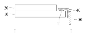
도 1b는 도 1a의 I-I 선에 따른 단면도이다.
도 2는 종래 기술에 따른 디스플레이 장치의 정전기 방전(ESD: Electrostatic Discharge) 구조를 나타내는 도면이다.
도 3은 본 발명의 실시 예들에 따른 디스플레이 장치의 개략적인 평면도이다.
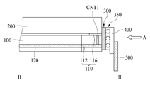
도 4a는 본 발명의 제1 실시 예에 따른 디스플레이 장치의 개략적인 도면을 나타내는 것으로, 도 3의 II-II 선에 따른 사이드 본딩 컨택 구조의 나타내는 도면이다.
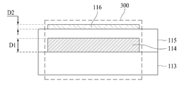
도 4b는 도 4a의 A방향에서 바라본 사이드 본딩 컨택 구조를 나타내는 도면이다.
도 5a는 본 발명의 제2 실시 예에 따른 디스플레이 장치의 개략적인 도면을 나타내는 것으로, 도 3의 II-II 선에 따른 사이드 본딩 컨택 구조의 나타내는 도면이다.
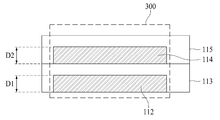
도 5b는 도 5a의 A방향에서 바라본 사이드 본딩 컨택 구조를 나타내는 도면이다.
도 6a 및 도 6b는 본 발명의 제3 실시 예에 따른 디스플레이 장치의 개략적인 도면을 나타내는 것으로, 도 3의 II-II 선에 따른 사이드 본딩 컨택 구조의 나타내는 도면이다.
도 6c는 도 6a 또는 도 6b의 A방향에서 바라본 사이드 본딩 컨택 구조를 나타내는 도면이다.
도 7a 및 도 7b는 본 발명의 제4 실시 예에 따른 디스플레이 장치의 개략적인 도면을 나타내는 것으로, 도 3의 II-II 선에 따른 사이드 본딩 컨택 구조를 나타내는 도면이다.
도 8은 도 7a 또는 도 7b의 B방향에서 바라본 사이드 본딩 컨택 구조를 나타내는 것으로, 제1 기판에 배치된 복수의 신호 패드와 복수의 배선을 나타내는 도면이다.
도 9는 도 7a 또는 도 7b의 A방향에서 바라본 사이드 본딩 컨택 구조를 나타내는 것으로, 도 8에 도시된 그라인딩 라인을 따라 절개된 단면을 나타내는 도면이다.
도 10은 본 발명의 제5 실시 예에 따른 디스플레이 장치의 개략적인 단면도이다.
도 11은 도 10에 도시된 A부분을 확대한 도면이다.
도 12a는 도 10의 B방향에서 바라본 사이드 본딩 컨택 구조 및 정전기 방전(ESD) 구조를 나타내는 도면이다.
도 12b는 디스플레이 패널의 측면에 도전성 차광부가 부착된 것을 나타내는 도면이다.
도 13은 본 발명의 실시 예들에 따른 디스플레이 장치를 타일 형태로 배치하여 비디오 월 디스플레이 장치를 구성한 것을 나타내는 도면이다.
110: 신호 패드
200, 1200: 제2 기판
300: 연결 전극
350: 접착층
400: 연성 회로 필름
500: 인쇄 회로 기판
1000: 디스플레이 장치
1300: 접지 전극
1400: 도전성 차광부
1500: 메탈 프레임
1600: 탄성 레진
Claims (12)
- 화면이 표시되는 액티브 영역과 복수의 패드가 배치된 패드 영역을 포함하는 디스플레이 장치에 있어서,
서로 마주하는 제1 기판과 제2 기판;
상기 제1 기판에 배치된 신호 패드;
상기 신호 패드의 일 측면과 연결된 연결 전극; 및
상기 연결 전극과 연결되는 연성 회로 필름을 포함하고,
상기 신호 패드는 절연막을 사이에 두고 배치된 복수의 라인을 포함하고, 상기 복수의 라인이 전기적으로 연결된 디스플레이 장치. - 제1 항에 있어서,
상기 복수의 라인은,
상기 액티브 영역에 배치된 게이트 라인과 동일 층에 배치된 제1 라인,
상기 액티브 영역에 배치된 데이터 라인과 동일 층에 배치된 제2 라인 및
상기 액티브 영역에 배치된 픽셀 전극과 동일 층에 배치된 제3 라인 중 적어도 2개의 라인을 포함하는 디스플레이 장치. - 제2 항에 있어서,
상기 제1 라인과 상기 제2 라인 사이에는 제1 절연막이 배치되고,
상기 제1 라인과 상기 제2 라인은 제1 컨택홀을 통해 전기적으로 연결되고,
상기 제2 라인과 상기 제3 라인 사이에는 제2 절연막이 배치되고,
상기 제2 라인과 상기 제3 라인은 제2 컨택홀을 통해 전기적으로 연결된 디스플레이 장치. - 제3 항에 있어서,
상기 연결 전극이 상기 제1 기판의 측면 및 상기 제2 기판의 측면에 배치된 디스플레이 장치. - 제4 항에 있어서,
상기 제1 기판과 제2 기판의 일 측면에서 상기 제1 라인 및 상기 제2 라인과 상기 연결 전극이 전기적으로 연결된 디스플레이 장치. - 제4 항에 있어서,
상기 제1 기판과 제2 기판의 일 측면에서 상기 제1 라인 및 상기 제3 라인과 상기 연결 전극이 전기적으로 연결된 디스플레이 장치. - 제4 항에 있어서,
상기 제1 기판과 제2 기판의 일 측면에서 상기 제2 라인 및 상기 제3 라인과 상기 연결 전극이 전기적으로 연결된 디스플레이 장치. - 제4 항에 있어서,
상기 제1 기판과 제2 기판의 일 측면에서 상기 제1 라인, 상기 제2 라인 및 상기 제3 라인과 상기 연결 전극이 전기적으로 연결된 디스플레이 장치. - 제5 항 내지 제8 항 중 어느 한 항에 있어서,
상기 연성 회로 필름이 접착층에 의해서 상기 제1 기판의 측면 및 상기 제2 기판의 측면에 배치된 디스플레이 장치. - 제9 항에 있어서,
상기 제2 기판 상에 배치된 정전기 방전층; 및
상기 정전기 방전층과 전기적으로 접속되고, 상기 제1 기판의 측면 및 상기 제2 기판의 측면에 배치된 복수의 접지 전극;을 더 포함하는 디스플레이 장치. - 제10 항에 있어서,
상기 제1 기판 및 제2 기판이 안착되는 메탈 프레임; 및
상기 복수의 접지 전극과, 상기 제1 기판의 측면 및 상기 제2 기판의 측면을 덮도록 배치된 도전성 차광부;를 더 포함하고,
상기 도전성 차광부가 상기 메탈 프레임의 외부 측벽에 부착되어 상기 복수의 접지 전극과 상기 메탈 프레임이 전기적으로 연결된 디스플레이 장치. - 제11 항에 있어서,
상기 도전성 차광부는,
상기 메탈 프레임의 외부 측벽 및 상기 복수의 접지 전극에 부착된 도전성 접착층과,
상기 도전성 접착층 상에 배치된 메탈 필름과,
상기 메탈 필름 상에 배치된 차광 필름을 포함하여 구성되고,
상기 도전성 차광부가 연성 회로 필름을 덮도록 배치된 디스플레이 장치.
Priority Applications (6)
| Application Number | Priority Date | Filing Date | Title |
|---|---|---|---|
| KR1020150095395A KR102387880B1 (ko) | 2015-07-03 | 2015-07-03 | 디스플레이 장치 |
| EP16177157.1A EP3112931B1 (en) | 2015-07-03 | 2016-06-30 | Display device |
| CN201610512128.5A CN106324927B (zh) | 2015-07-03 | 2016-07-01 | 显示装置 |
| US15/200,787 US9947652B2 (en) | 2015-07-03 | 2016-07-01 | Display device |
| US15/913,478 US10170462B2 (en) | 2015-07-03 | 2018-03-06 | Display device |
| KR1020220045787A KR102522555B1 (ko) | 2015-07-03 | 2022-04-13 | 디스플레이 장치 |
Applications Claiming Priority (1)
| Application Number | Priority Date | Filing Date | Title |
|---|---|---|---|
| KR1020150095395A KR102387880B1 (ko) | 2015-07-03 | 2015-07-03 | 디스플레이 장치 |
Related Child Applications (1)
| Application Number | Title | Priority Date | Filing Date |
|---|---|---|---|
| KR1020220045787A Division KR102522555B1 (ko) | 2015-07-03 | 2022-04-13 | 디스플레이 장치 |
Publications (2)
| Publication Number | Publication Date |
|---|---|
| KR20170005341A true KR20170005341A (ko) | 2017-01-12 |
| KR102387880B1 KR102387880B1 (ko) | 2022-04-18 |
Family
ID=56360203
Family Applications (2)
| Application Number | Title | Priority Date | Filing Date |
|---|---|---|---|
| KR1020150095395A Active KR102387880B1 (ko) | 2015-07-03 | 2015-07-03 | 디스플레이 장치 |
| KR1020220045787A Active KR102522555B1 (ko) | 2015-07-03 | 2022-04-13 | 디스플레이 장치 |
Family Applications After (1)
| Application Number | Title | Priority Date | Filing Date |
|---|---|---|---|
| KR1020220045787A Active KR102522555B1 (ko) | 2015-07-03 | 2022-04-13 | 디스플레이 장치 |
Country Status (4)
| Country | Link |
|---|---|
| US (2) | US9947652B2 (ko) |
| EP (1) | EP3112931B1 (ko) |
| KR (2) | KR102387880B1 (ko) |
| CN (1) | CN106324927B (ko) |
Cited By (15)
| Publication number | Priority date | Publication date | Assignee | Title |
|---|---|---|---|---|
| KR20190076091A (ko) * | 2017-12-21 | 2019-07-02 | 삼성디스플레이 주식회사 | 표시장치 |
| US10578901B2 (en) | 2017-04-25 | 2020-03-03 | Samsung Display Co. Ltd. | Display device |
| KR20200053012A (ko) * | 2018-11-07 | 2020-05-18 | 삼성디스플레이 주식회사 | 유기 발광 표시 장치 |
| KR20200081728A (ko) * | 2018-12-28 | 2020-07-08 | 엘지디스플레이 주식회사 | 표시장치 |
| KR20200083859A (ko) * | 2018-12-31 | 2020-07-09 | 삼성디스플레이 주식회사 | 표시 장치 |
| KR20200111862A (ko) * | 2019-03-19 | 2020-10-05 | 삼성디스플레이 주식회사 | 표시 장치 및 이의 제조 방법 |
| KR20200115769A (ko) * | 2019-03-25 | 2020-10-08 | 삼성디스플레이 주식회사 | 표시 장치 및 그 제조 방법 |
| KR20210002287A (ko) * | 2019-06-28 | 2021-01-07 | 삼성디스플레이 주식회사 | 표시 장치 및 그 제조 방법 |
| US10950684B2 (en) | 2019-07-22 | 2021-03-16 | Samsung Display Co., Ltd. | Display apparatus |
| KR20210054883A (ko) * | 2019-11-06 | 2021-05-14 | 한국유리공업 주식회사 | 유리 조립체 |
| CN113453527A (zh) * | 2020-03-27 | 2021-09-28 | 三星显示有限公司 | 制造显示设备的方法 |
| US11139360B2 (en) | 2017-12-28 | 2021-10-05 | Samsung Display Co., Ltd. | Display panel including display signal pads and sensing signal pads mounted on the display panel sidewall |
| US11262625B2 (en) | 2019-09-02 | 2022-03-01 | Samsung Display Co., Ltd. | Display device |
| KR20220093061A (ko) * | 2017-09-25 | 2022-07-05 | 삼성디스플레이 주식회사 | 표시패널 |
| US11710813B2 (en) | 2019-05-03 | 2023-07-25 | Samsung Electronics Co., Ltd. | Light emitting diode module |
Families Citing this family (46)
| Publication number | Priority date | Publication date | Assignee | Title |
|---|---|---|---|---|
| KR102378891B1 (ko) * | 2015-09-18 | 2022-03-24 | 엘지디스플레이 주식회사 | 디스플레이 패널 및 이를 포함하는 디스플레이 장치 |
| KR102626385B1 (ko) | 2016-06-08 | 2024-01-19 | 삼성디스플레이 주식회사 | 표시장치 및 이의 제조방법 |
| JP6956475B2 (ja) * | 2016-09-28 | 2021-11-02 | エルジー ディスプレイ カンパニー リミテッド | 電子部品の実装方法、電子部品の接合構造、基板装置、ディスプレイ装置、ディスプレイシステム |
| JP6726070B2 (ja) | 2016-09-28 | 2020-07-22 | エルジー ディスプレイ カンパニー リミテッド | 電子部品の実装方法、電子部品の接合構造、基板装置、ディスプレイ装置、ディスプレイシステム |
| KR102772195B1 (ko) * | 2017-02-28 | 2025-02-26 | 삼성디스플레이 주식회사 | 표시 장치 및 표시 장치의 제조 방법 |
| TWI621900B (zh) * | 2017-04-28 | 2018-04-21 | 友達光電股份有限公司 | 顯示裝置與其製作方法 |
| KR102350908B1 (ko) * | 2017-06-12 | 2022-01-14 | 삼성디스플레이 주식회사 | 표시 장치 |
| CN107145015B (zh) * | 2017-06-30 | 2020-08-07 | 武汉华星光电技术有限公司 | 一种显示面板 |
| KR102408902B1 (ko) * | 2017-08-16 | 2022-06-15 | 엘지디스플레이 주식회사 | 디스플레이 장치 |
| CN109426018A (zh) * | 2017-08-22 | 2019-03-05 | 京东方科技集团股份有限公司 | 基板及其制造方法、显示面板、拼接屏 |
| CN107402466B (zh) * | 2017-08-31 | 2021-01-26 | Tcl华星光电技术有限公司 | 液晶显示面板的邦定方法与液晶显示面板邦定结构 |
| CN107703663A (zh) * | 2017-09-26 | 2018-02-16 | 张家港康得新光电材料有限公司 | 2d/3d可切换面板及显示装置 |
| CN107643634A (zh) * | 2017-10-26 | 2018-01-30 | 深圳市华星光电半导体显示技术有限公司 | 一种像素单元及显示基板 |
| KR102433358B1 (ko) * | 2017-12-05 | 2022-08-16 | 엘지디스플레이 주식회사 | 표시 장치 |
| KR20190083027A (ko) * | 2018-01-02 | 2019-07-11 | 삼성디스플레이 주식회사 | 표시패널 및 그 제조방법 |
| US11018174B2 (en) * | 2018-01-22 | 2021-05-25 | Semiconductor Components Industries, Llc | Apparatus and method related to sensor die ESD protection |
| CN108957878B (zh) * | 2018-07-19 | 2022-03-11 | 武汉天马微电子有限公司 | 显示模组及其制备方法和显示装置 |
| KR102731395B1 (ko) * | 2018-08-14 | 2024-11-18 | 삼성디스플레이 주식회사 | 표시장치 및 그 제조방법 |
| KR102657409B1 (ko) * | 2018-12-20 | 2024-04-16 | 엘지디스플레이 주식회사 | 표시패널 및 표시장치 |
| KR102713260B1 (ko) * | 2018-12-26 | 2024-10-04 | 삼성디스플레이 주식회사 | 표시 장치 |
| TWI685828B (zh) * | 2019-01-03 | 2020-02-21 | 友達光電股份有限公司 | 顯示裝置 |
| CN110119054B (zh) * | 2019-04-25 | 2022-02-22 | Tcl华星光电技术有限公司 | 显示面板 |
| KR20200127815A (ko) * | 2019-05-03 | 2020-11-11 | 삼성전자주식회사 | 발광 다이오드 모듈 및 이를 포함하는 디스플레이 장치 |
| KR102787781B1 (ko) | 2019-10-07 | 2025-03-27 | 삼성디스플레이 주식회사 | 표시 장치 |
| CN110764295A (zh) * | 2019-10-14 | 2020-02-07 | 深圳市华星光电半导体显示技术有限公司 | 液晶显示面板及液晶模组 |
| CN110837194B (zh) * | 2019-10-30 | 2022-04-26 | 深圳市华星光电半导体显示技术有限公司 | 一种液晶显示装置、拼接屏 |
| CN110718156B (zh) * | 2019-10-31 | 2022-08-19 | 京东方科技集团股份有限公司 | 可折叠显示面板及制作方法、显示装置 |
| KR20210073649A (ko) * | 2019-12-10 | 2021-06-21 | 삼성디스플레이 주식회사 | 유기 발광 표시 장치 및 유기 발광 표시 장치의 제조 방법 |
| KR102945401B1 (ko) * | 2019-12-19 | 2026-03-31 | 삼성디스플레이 주식회사 | 표시 장치 |
| KR20210109087A (ko) | 2020-02-26 | 2021-09-06 | 삼성디스플레이 주식회사 | 표시 장치 |
| CN113823185B (zh) * | 2020-06-19 | 2023-09-12 | 群创光电股份有限公司 | 电子装置 |
| KR102914090B1 (ko) * | 2020-07-03 | 2026-01-19 | 삼성디스플레이 주식회사 | 표시장치 |
| MY199608A (en) * | 2020-07-31 | 2023-11-09 | Samsung Electronics Co Ltd | Electronic device including conductive member |
| CN113674614B (zh) * | 2020-08-14 | 2023-03-21 | 友达光电股份有限公司 | 显示装置及其制造方法 |
| CN113284416B (zh) * | 2020-08-14 | 2023-03-10 | 友达光电股份有限公司 | 显示面板 |
| KR102887784B1 (ko) * | 2020-10-27 | 2025-11-19 | 삼성전자주식회사 | 디스플레이 장치 및 이의 제조방법 |
| CN114582220B (zh) * | 2020-11-30 | 2025-04-29 | 京东方科技集团股份有限公司 | 显示母板及其制造方法、显示基板、显示面板 |
| US11515271B2 (en) * | 2021-01-27 | 2022-11-29 | Innolux Corporation | Electronic device including wire on side surface of substrate and manufacturing method thereof |
| CN114815407B (zh) * | 2021-01-28 | 2024-08-27 | 京东方科技集团股份有限公司 | 显示基板及其制备方法、显示面板 |
| CN115145065B (zh) * | 2021-03-31 | 2025-04-08 | 京东方科技集团股份有限公司 | 显示面板及其制备方法、显示装置和拼接显示装置 |
| EP4332948A4 (en) * | 2021-10-27 | 2024-11-06 | Samsung Electronics Co., Ltd. | Display device including display module and method for manufacturing same |
| CN115036329B (zh) * | 2022-04-15 | 2025-05-02 | 合肥京东方显示技术有限公司 | 一种显示基板、显示基板的制作方法及显示装置 |
| US11662861B1 (en) * | 2022-04-29 | 2023-05-30 | Dell Products L.P. | Edge display having electrostatic discharge protection |
| CN114935858A (zh) * | 2022-05-26 | 2022-08-23 | Tcl华星光电技术有限公司 | 液晶显示装置及其制造方法 |
| CN116110927B (zh) * | 2023-03-28 | 2025-07-22 | 天马新型显示技术研究院(厦门)有限公司 | 显示面板和显示装置 |
| KR20250128684A (ko) * | 2024-02-21 | 2025-08-28 | 엘지디스플레이 주식회사 | 표시 장치 |
Citations (4)
| Publication number | Priority date | Publication date | Assignee | Title |
|---|---|---|---|---|
| KR20060053923A (ko) * | 2004-08-06 | 2006-05-22 | 미쓰비시덴키 가부시키가이샤 | 액정 표시장치 및 그 제조방법 |
| KR20120045983A (ko) * | 2010-10-29 | 2012-05-09 | 엘지디스플레이 주식회사 | 전기영동 표시장치 |
| KR20140136238A (ko) * | 2013-05-20 | 2014-11-28 | 엘지전자 주식회사 | 디스플레이 패널 및 그를 포함하는 디스플레이 장치 |
| KR20150026033A (ko) * | 2013-08-30 | 2015-03-11 | 엘지디스플레이 주식회사 | 액정 표시 장치 및 그의 제조 방법 |
Family Cites Families (6)
| Publication number | Priority date | Publication date | Assignee | Title |
|---|---|---|---|---|
| KR20080024826A (ko) * | 2006-09-15 | 2008-03-19 | 삼성전자주식회사 | 액정표시장치 |
| US20150177542A1 (en) * | 2012-11-29 | 2015-06-25 | Kyocera Corporation | Display apparatus |
| KR101931248B1 (ko) * | 2012-12-27 | 2019-03-13 | 엘지디스플레이 주식회사 | 표시장치 및 그 제조방법 |
| US8994042B2 (en) * | 2013-05-20 | 2015-03-31 | Lg Electronics Inc. | Display panel and display device |
| KR102145961B1 (ko) * | 2013-12-18 | 2020-08-20 | 삼성디스플레이 주식회사 | 유기 발광 표시 장치 |
| CN103700782B (zh) * | 2013-12-26 | 2015-12-09 | 合肥京东方光电科技有限公司 | 一种oled显示面板及其制备方法 |
-
2015
- 2015-07-03 KR KR1020150095395A patent/KR102387880B1/ko active Active
-
2016
- 2016-06-30 EP EP16177157.1A patent/EP3112931B1/en active Active
- 2016-07-01 US US15/200,787 patent/US9947652B2/en active Active
- 2016-07-01 CN CN201610512128.5A patent/CN106324927B/zh active Active
-
2018
- 2018-03-06 US US15/913,478 patent/US10170462B2/en active Active
-
2022
- 2022-04-13 KR KR1020220045787A patent/KR102522555B1/ko active Active
Patent Citations (4)
| Publication number | Priority date | Publication date | Assignee | Title |
|---|---|---|---|---|
| KR20060053923A (ko) * | 2004-08-06 | 2006-05-22 | 미쓰비시덴키 가부시키가이샤 | 액정 표시장치 및 그 제조방법 |
| KR20120045983A (ko) * | 2010-10-29 | 2012-05-09 | 엘지디스플레이 주식회사 | 전기영동 표시장치 |
| KR20140136238A (ko) * | 2013-05-20 | 2014-11-28 | 엘지전자 주식회사 | 디스플레이 패널 및 그를 포함하는 디스플레이 장치 |
| KR20150026033A (ko) * | 2013-08-30 | 2015-03-11 | 엘지디스플레이 주식회사 | 액정 표시 장치 및 그의 제조 방법 |
Cited By (18)
| Publication number | Priority date | Publication date | Assignee | Title |
|---|---|---|---|---|
| US10578901B2 (en) | 2017-04-25 | 2020-03-03 | Samsung Display Co. Ltd. | Display device |
| KR20220093061A (ko) * | 2017-09-25 | 2022-07-05 | 삼성디스플레이 주식회사 | 표시패널 |
| KR20190076091A (ko) * | 2017-12-21 | 2019-07-02 | 삼성디스플레이 주식회사 | 표시장치 |
| US11672151B2 (en) | 2017-12-28 | 2023-06-06 | Samsung Display Co., Ltd. | Display panel including display signal pads and sensing signal pads mounted on the display panel sidewall |
| US11139360B2 (en) | 2017-12-28 | 2021-10-05 | Samsung Display Co., Ltd. | Display panel including display signal pads and sensing signal pads mounted on the display panel sidewall |
| US12022707B2 (en) | 2017-12-28 | 2024-06-25 | Samsung Display Co., Ltd. | Display panel including display signal pads and sensing signal pads mounted on the display panel sidewall |
| KR20200053012A (ko) * | 2018-11-07 | 2020-05-18 | 삼성디스플레이 주식회사 | 유기 발광 표시 장치 |
| KR20200081728A (ko) * | 2018-12-28 | 2020-07-08 | 엘지디스플레이 주식회사 | 표시장치 |
| KR20200083859A (ko) * | 2018-12-31 | 2020-07-09 | 삼성디스플레이 주식회사 | 표시 장치 |
| KR20200111862A (ko) * | 2019-03-19 | 2020-10-05 | 삼성디스플레이 주식회사 | 표시 장치 및 이의 제조 방법 |
| KR20200115769A (ko) * | 2019-03-25 | 2020-10-08 | 삼성디스플레이 주식회사 | 표시 장치 및 그 제조 방법 |
| US11710813B2 (en) | 2019-05-03 | 2023-07-25 | Samsung Electronics Co., Ltd. | Light emitting diode module |
| KR20210002287A (ko) * | 2019-06-28 | 2021-01-07 | 삼성디스플레이 주식회사 | 표시 장치 및 그 제조 방법 |
| US10950684B2 (en) | 2019-07-22 | 2021-03-16 | Samsung Display Co., Ltd. | Display apparatus |
| US11262625B2 (en) | 2019-09-02 | 2022-03-01 | Samsung Display Co., Ltd. | Display device |
| KR20210054883A (ko) * | 2019-11-06 | 2021-05-14 | 한국유리공업 주식회사 | 유리 조립체 |
| KR20210121351A (ko) * | 2020-03-27 | 2021-10-08 | 삼성디스플레이 주식회사 | 본딩 장치 및 그것을 이용한 표시 장치의 제조 방법 |
| CN113453527A (zh) * | 2020-03-27 | 2021-09-28 | 三星显示有限公司 | 制造显示设备的方法 |
Also Published As
| Publication number | Publication date |
|---|---|
| KR102522555B1 (ko) | 2023-04-14 |
| KR102387880B1 (ko) | 2022-04-18 |
| KR20220052884A (ko) | 2022-04-28 |
| EP3112931B1 (en) | 2019-12-18 |
| CN106324927B (zh) | 2019-11-29 |
| US9947652B2 (en) | 2018-04-17 |
| CN106324927A (zh) | 2017-01-11 |
| US10170462B2 (en) | 2019-01-01 |
| US20180197849A1 (en) | 2018-07-12 |
| EP3112931A1 (en) | 2017-01-04 |
| US20170005083A1 (en) | 2017-01-05 |
Similar Documents
| Publication | Publication Date | Title |
|---|---|---|
| KR102522555B1 (ko) | 디스플레이 장치 | |
| KR102698003B1 (ko) | 디스플레이 장치 및 그 제조 방법 | |
| GB2542503B (en) | Display device | |
| TWI638211B (zh) | Display device | |
| KR20240129149A (ko) | 디스플레이 장치 및 그 제조 방법 | |
| JP5454872B2 (ja) | 液晶装置、電子機器 | |
| US10168591B2 (en) | Liquid crystal display device | |
| KR20130003893A (ko) | 액정 표시 장치 | |
| WO2019000912A1 (zh) | 显示面板及其制造方法、显示装置 | |
| TW201533640A (zh) | 防靜電觸控面板 | |
| US9798206B2 (en) | Liquid crystal display apparatus | |
| KR20170025963A (ko) | 연성 인쇄 회로 필름 및 그를 이용한 디스플레이 장치 | |
| KR20210101359A (ko) | 전자패널 및 이를 포함한 표시장치 | |
| KR20170005254A (ko) | 디스플레이 장치 | |
| KR102868942B1 (ko) | 입력 감지 패널 및 이를 포함하는 표시 장치 | |
| KR102522706B1 (ko) | 표시 장치 | |
| CN114967253A (zh) | 阵列基板、显示面板及显示装置 | |
| TWI674523B (zh) | 觸控顯示裝置 | |
| KR102227163B1 (ko) | 표시 장치 | |
| JP2011053327A (ja) | 表示装置 | |
| KR102787781B1 (ko) | 표시 장치 | |
| KR102573913B1 (ko) | 박형 기판을 포함하는 디스플레이 장치 | |
| KR20220045821A (ko) | 표시장치 | |
| JP2021043420A (ja) | 表示装置 |
Legal Events
| Date | Code | Title | Description |
|---|---|---|---|
| PA0109 | Patent application |
St.27 status event code: A-0-1-A10-A12-nap-PA0109 |
|
| PG1501 | Laying open of application |
St.27 status event code: A-1-1-Q10-Q12-nap-PG1501 |
|
| P22-X000 | Classification modified |
St.27 status event code: A-2-2-P10-P22-nap-X000 |
|
| A201 | Request for examination | ||
| PA0201 | Request for examination |
St.27 status event code: A-1-2-D10-D11-exm-PA0201 |
|
| D13-X000 | Search requested |
St.27 status event code: A-1-2-D10-D13-srh-X000 |
|
| D14-X000 | Search report completed |
St.27 status event code: A-1-2-D10-D14-srh-X000 |
|
| E902 | Notification of reason for refusal | ||
| PE0902 | Notice of grounds for rejection |
St.27 status event code: A-1-2-D10-D21-exm-PE0902 |
|
| P11-X000 | Amendment of application requested |
St.27 status event code: A-2-2-P10-P11-nap-X000 |
|
| P13-X000 | Application amended |
St.27 status event code: A-2-2-P10-P13-nap-X000 |
|
| E701 | Decision to grant or registration of patent right | ||
| PE0701 | Decision of registration |
St.27 status event code: A-1-2-D10-D22-exm-PE0701 |
|
| A107 | Divisional application of patent | ||
| GRNT | Written decision to grant | ||
| PA0107 | Divisional application |
St.27 status event code: A-0-1-A10-A18-div-PA0107 St.27 status event code: A-0-1-A10-A16-div-PA0107 |
|
| PR0701 | Registration of establishment |
St.27 status event code: A-2-4-F10-F11-exm-PR0701 |
|
| PR1002 | Payment of registration fee |
St.27 status event code: A-2-2-U10-U11-oth-PR1002 Fee payment year number: 1 |
|
| PG1601 | Publication of registration |
St.27 status event code: A-4-4-Q10-Q13-nap-PG1601 |
|
| P22-X000 | Classification modified |
St.27 status event code: A-4-4-P10-P22-nap-X000 |
|
| P22-X000 | Classification modified |
St.27 status event code: A-4-4-P10-P22-nap-X000 |
|
| PR1001 | Payment of annual fee |
St.27 status event code: A-4-4-U10-U11-oth-PR1001 Fee payment year number: 4 |
|
| PR1001 | Payment of annual fee |
St.27 status event code: A-4-4-U10-U11-oth-PR1001 Fee payment year number: 5 |
|
| U11 | Full renewal or maintenance fee paid |
Free format text: ST27 STATUS EVENT CODE: A-4-4-U10-U11-OTH-PR1001 (AS PROVIDED BY THE NATIONAL OFFICE) Year of fee payment: 5 |