KR20170007429A - 구조화된 특징부를 갖는 이종 재료의 복합 구조체를 형성하기 위한 스탬핑 - Google Patents
구조화된 특징부를 갖는 이종 재료의 복합 구조체를 형성하기 위한 스탬핑 Download PDFInfo
- Publication number
- KR20170007429A KR20170007429A KR1020167035155A KR20167035155A KR20170007429A KR 20170007429 A KR20170007429 A KR 20170007429A KR 1020167035155 A KR1020167035155 A KR 1020167035155A KR 20167035155 A KR20167035155 A KR 20167035155A KR 20170007429 A KR20170007429 A KR 20170007429A
- Authority
- KR
- South Korea
- Prior art keywords
- base
- structured
- optical
- stamping
- feature
- Prior art date
- Legal status (The legal status is an assumption and is not a legal conclusion. Google has not performed a legal analysis and makes no representation as to the accuracy of the status listed.)
- Ceased
Links
Images











Classifications
-
- G—PHYSICS
- G02—OPTICS
- G02B—OPTICAL ELEMENTS, SYSTEMS OR APPARATUS
- G02B6/00—Light guides; Structural details of arrangements comprising light guides and other optical elements, e.g. couplings
- G02B6/24—Coupling light guides
- G02B6/42—Coupling light guides with opto-electronic elements
- G02B6/4201—Packages, e.g. shape, construction, internal or external details
- G02B6/4204—Packages, e.g. shape, construction, internal or external details the coupling comprising intermediate optical elements, e.g. lenses, holograms
- G02B6/4214—Packages, e.g. shape, construction, internal or external details the coupling comprising intermediate optical elements, e.g. lenses, holograms the intermediate optical element having redirecting reflective means, e.g. mirrors, prisms for deflecting the radiation from horizontal to down- or upward direction toward a device
-
- B—PERFORMING OPERATIONS; TRANSPORTING
- B21—MECHANICAL METAL-WORKING WITHOUT ESSENTIALLY REMOVING MATERIAL; PUNCHING METAL
- B21D—WORKING OR PROCESSING OF SHEET METAL OR METAL TUBES, RODS OR PROFILES WITHOUT ESSENTIALLY REMOVING MATERIAL; PUNCHING METAL
- B21D22/00—Shaping without cutting, by stamping, spinning, or deep-drawing
- B21D22/02—Stamping using rigid devices or tools
-
- B—PERFORMING OPERATIONS; TRANSPORTING
- B26—HAND CUTTING TOOLS; CUTTING; SEVERING
- B26F—PERFORATING; PUNCHING; CUTTING-OUT; STAMPING-OUT; SEVERING BY MEANS OTHER THAN CUTTING
- B26F1/00—Perforating; Punching; Cutting-out; Stamping-out; Apparatus therefor
- B26F1/38—Cutting-out; Stamping-out
- B26F1/40—Cutting-out; Stamping-out using a press, e.g. of the ram type
-
- B—PERFORMING OPERATIONS; TRANSPORTING
- B26—HAND CUTTING TOOLS; CUTTING; SEVERING
- B26F—PERFORATING; PUNCHING; CUTTING-OUT; STAMPING-OUT; SEVERING BY MEANS OTHER THAN CUTTING
- B26F1/00—Perforating; Punching; Cutting-out; Stamping-out; Apparatus therefor
- B26F1/38—Cutting-out; Stamping-out
- B26F1/44—Cutters therefor; Dies therefor
-
- G—PHYSICS
- G01—MEASURING; TESTING
- G01M—TESTING STATIC OR DYNAMIC BALANCE OF MACHINES OR STRUCTURES; TESTING OF STRUCTURES OR APPARATUS, NOT OTHERWISE PROVIDED FOR
- G01M11/00—Testing of optical apparatus; Testing structures by optical methods not otherwise provided for
- G01M11/02—Testing optical properties
- G01M11/04—Optical benches therefor
-
- G—PHYSICS
- G02—OPTICS
- G02B—OPTICAL ELEMENTS, SYSTEMS OR APPARATUS
- G02B6/00—Light guides; Structural details of arrangements comprising light guides and other optical elements, e.g. couplings
- G02B6/24—Coupling light guides
- G02B6/36—Mechanical coupling means
- G02B6/3616—Holders, macro size fixtures for mechanically holding or positioning fibres, e.g. on an optical bench
-
- G—PHYSICS
- G02—OPTICS
- G02B—OPTICAL ELEMENTS, SYSTEMS OR APPARATUS
- G02B6/00—Light guides; Structural details of arrangements comprising light guides and other optical elements, e.g. couplings
- G02B6/24—Coupling light guides
- G02B6/42—Coupling light guides with opto-electronic elements
- G02B6/4201—Packages, e.g. shape, construction, internal or external details
- G02B6/4219—Mechanical fixtures for holding or positioning the elements relative to each other in the couplings; Alignment methods for the elements, e.g. measuring or observing methods especially used therefor
- G02B6/4228—Passive alignment, i.e. without a detection of the degree of coupling or the position of the elements
- G02B6/423—Passive alignment, i.e. without a detection of the degree of coupling or the position of the elements using guiding surfaces for the alignment
-
- B—PERFORMING OPERATIONS; TRANSPORTING
- B26—HAND CUTTING TOOLS; CUTTING; SEVERING
- B26F—PERFORATING; PUNCHING; CUTTING-OUT; STAMPING-OUT; SEVERING BY MEANS OTHER THAN CUTTING
- B26F1/00—Perforating; Punching; Cutting-out; Stamping-out; Apparatus therefor
- B26F1/38—Cutting-out; Stamping-out
- B26F1/40—Cutting-out; Stamping-out using a press, e.g. of the ram type
- B26F2001/407—Cutting-out; Stamping-out using a press, e.g. of the ram type stepwise sequential punching processes
-
- G—PHYSICS
- G02—OPTICS
- G02B—OPTICAL ELEMENTS, SYSTEMS OR APPARATUS
- G02B6/00—Light guides; Structural details of arrangements comprising light guides and other optical elements, e.g. couplings
- G02B6/24—Coupling light guides
- G02B6/36—Mechanical coupling means
- G02B6/3628—Mechanical coupling means for mounting fibres to supporting carriers
- G02B6/3648—Supporting carriers of a microbench type, i.e. with micromachined additional mechanical structures
- G02B6/3652—Supporting carriers of a microbench type, i.e. with micromachined additional mechanical structures the additional structures being prepositioning mounting areas, allowing only movement in one dimension, e.g. grooves, trenches or vias in the microbench surface, i.e. self aligning supporting carriers
-
- G—PHYSICS
- G02—OPTICS
- G02B—OPTICAL ELEMENTS, SYSTEMS OR APPARATUS
- G02B6/00—Light guides; Structural details of arrangements comprising light guides and other optical elements, e.g. couplings
- G02B6/24—Coupling light guides
- G02B6/36—Mechanical coupling means
- G02B6/3628—Mechanical coupling means for mounting fibres to supporting carriers
- G02B6/3684—Mechanical coupling means for mounting fibres to supporting carriers characterised by the manufacturing process of surface profiling of the supporting carrier
- G02B6/3696—Mechanical coupling means for mounting fibres to supporting carriers characterised by the manufacturing process of surface profiling of the supporting carrier by moulding, e.g. injection moulding, casting, embossing, stamping, stenciling, printing, or with metallic mould insert manufacturing using LIGA or MIGA techniques
-
- G—PHYSICS
- G02—OPTICS
- G02B—OPTICAL ELEMENTS, SYSTEMS OR APPARATUS
- G02B6/00—Light guides; Structural details of arrangements comprising light guides and other optical elements, e.g. couplings
- G02B6/24—Coupling light guides
- G02B6/42—Coupling light guides with opto-electronic elements
- G02B6/4201—Packages, e.g. shape, construction, internal or external details
- G02B6/4219—Mechanical fixtures for holding or positioning the elements relative to each other in the couplings; Alignment methods for the elements, e.g. measuring or observing methods especially used therefor
- G02B6/4236—Fixing or mounting methods of the aligned elements
- G02B6/424—Mounting of the optical light guide
- G02B6/4243—Mounting of the optical light guide into a groove
-
- G—PHYSICS
- G02—OPTICS
- G02B—OPTICAL ELEMENTS, SYSTEMS OR APPARATUS
- G02B6/00—Light guides; Structural details of arrangements comprising light guides and other optical elements, e.g. couplings
- G02B6/24—Coupling light guides
- G02B6/42—Coupling light guides with opto-electronic elements
- G02B6/4201—Packages, e.g. shape, construction, internal or external details
- G02B6/4219—Mechanical fixtures for holding or positioning the elements relative to each other in the couplings; Alignment methods for the elements, e.g. measuring or observing methods especially used therefor
- G02B6/4236—Fixing or mounting methods of the aligned elements
- G02B6/4245—Mounting of the opto-electronic elements
-
- G—PHYSICS
- G02—OPTICS
- G02B—OPTICAL ELEMENTS, SYSTEMS OR APPARATUS
- G02B6/00—Light guides; Structural details of arrangements comprising light guides and other optical elements, e.g. couplings
- G02B6/24—Coupling light guides
- G02B6/42—Coupling light guides with opto-electronic elements
- G02B6/4201—Packages, e.g. shape, construction, internal or external details
- G02B6/4246—Bidirectionally operating package structures
-
- G—PHYSICS
- G02—OPTICS
- G02B—OPTICAL ELEMENTS, SYSTEMS OR APPARATUS
- G02B6/00—Light guides; Structural details of arrangements comprising light guides and other optical elements, e.g. couplings
- G02B6/24—Coupling light guides
- G02B6/42—Coupling light guides with opto-electronic elements
- G02B6/4201—Packages, e.g. shape, construction, internal or external details
- G02B6/4249—Packages, e.g. shape, construction, internal or external details comprising arrays of active devices and fibres
-
- G—PHYSICS
- G02—OPTICS
- G02B—OPTICAL ELEMENTS, SYSTEMS OR APPARATUS
- G02B6/00—Light guides; Structural details of arrangements comprising light guides and other optical elements, e.g. couplings
- G02B6/24—Coupling light guides
- G02B6/42—Coupling light guides with opto-electronic elements
- G02B6/4201—Packages, e.g. shape, construction, internal or external details
- G02B6/4251—Sealed packages
Landscapes
- Physics & Mathematics (AREA)
- General Physics & Mathematics (AREA)
- Optics & Photonics (AREA)
- Mechanical Engineering (AREA)
- Engineering & Computer Science (AREA)
- Life Sciences & Earth Sciences (AREA)
- Forests & Forestry (AREA)
- Chemical & Material Sciences (AREA)
- Crystallography & Structural Chemistry (AREA)
- Analytical Chemistry (AREA)
- Optical Couplings Of Light Guides (AREA)
- Shaping Metal By Deep-Drawing, Or The Like (AREA)
- Casting Or Compression Moulding Of Plastics Or The Like (AREA)
- Laminated Bodies (AREA)
Abstract
Description
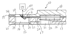
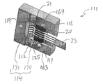
도 1a는 본 발명의 일 실시예에 따른 복합 구조체를 갖는 스탬핑된 광학 벤치를 갖는 광학 커플링 디바이스를 도시하고 있고; 도 1b는 그 분해도이고, 도 1c는 도 1b의 보조부의 영역의 확대도이고; 도 1d는 도 1a의 라인 1D-1D를 따라 취한 단면도이다.
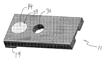
도 2a 내지 도 2d는 본 발명의 일 실시예에 따른 보조부의 다양한 도면을 도시하고 있다.
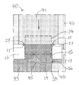
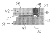
도 3a는 스탬핑에 의해 보조부를 형성하기 위한 인서트의 개략도이고; 도 3b는 본 발명의 일 실시예에 따른 스탬핑 공구의 부분을 개략적으로 도시하고 있고, 도 3c는 도 3b의 접촉 영역의 확대도이고, 도 3d는 스탬핑 작업이 실시된 후에 보조부 내의 플라스틱 스트레인의 시뮬레이션 도면이다.
도 4a 및 도 4b는 본 발명의 일 실시예에 따라 형성된 광학 벤치의 다양한 도면이고, 도 4c 및 도 4d는 본 발명의 일 실시예에 따라 형성된 광학 벤치의 다양한 이미지이다.
도 5a는 본 발명의 일 실시예에 따른 스탬핑 공구를 개략적으로 도시하고 있고; 도 5b는 도 5a의 라인 5B-5B를 따라 취한 단면도이고; 도 5c는 도 5b의 접촉 영역의 확대도이다.
도 6은 본 발명의 일 실시예에 따른 광학 벤치의 스탬핑을 위한 금속의 스트립의 사시도이다.
도 7a는 본 발명의 다른 실시예에 따른 복합 구조체를 갖는 광학 벤치의 사시도이고; 도 7b는 본 발명의 일 실시예에 따른 스탬핑 공구의 부분을 개략적으로 도시하고 있고; 도 7c는 도 7b의 접촉 영역의 확대도이다.
도 8a는 본 발명의 다른 실시예에 따른 복합 구조체를 갖는 스탬핑된 광학 벤치를 갖는 광학 커플링 디바이스를 도시하고 있고; 도 8b는 그 분해도이고, 도 8c는 도 8a의 라인 8C-8C를 따라 취한 단면도이다.
Claims (20)
- 광학 전송과 관련하여 광로를 규정하도록 그 위에 형성된 구조화된 특징부를 갖는 복합 구조체를 형성하는 방법이며,
제1 구조화된 특징부를 형성하는 제1 재료의 기부를 제공하는 단계,
상기 기부에 대해 제2 재료를 위치설정하는 단계로서, 상기 제2 재료는 상기 제1 재료에 대해 이종인, 제2 재료를 위치설정하는 단계, 및
상기 제2 재료를 상기 기부에 구조적으로 커플링하고 상기 제2 재료 상에 제2 구조화된 특징부를 형성하도록 상기 제2 재료를 스탬핑하여, 이에 의해 제1 재료의 기부 및 상기 제2 구조화된 특징부가 그 위에 형성되어 있는 제2 재료로부터의 보조부를 포함하는 복합 구조체를 형성하는 단계를 포함하고,
구조화된 특징부들은 광학 전송과 관련하여 광로를 규정하는, 복합 구조체 형성 방법. - 제1항에 있어서, 상기 제2 구조화된 특징부는 상기 제2 재료를 스탬핑함으로써 형성된 광학 요소를 포함하는, 복합 구조체 형성 방법.
- 제2항에 있어서, 상기 기부의 제1 구조화된 특징부는 상기 광로를 따라 상기 광학 요소와 광학 정렬되도록 광학 구성요소를 위치설정하는 것을 용이하게 하기 위한 제1 정렬 구조체를 포함하는, 복합 구조체 형성 방법.
- 제2항에 있어서, 상기 제2 구조화된 특징부는 상기 광로를 따라 상기 광학 요소와 광학 정렬되도록 광학 구성요소를 위치설정하는 것을 용이하게 하기 위한 제2 정렬 구조체를 더 포함하는, 복합 구조체 형성 방법.
- 제2항에 있어서, 상기 광학 요소는 상기 제2 재료를 스탬핑함으로써 형성된 구조화된 반사면을 포함하는, 복합 구조체 형성 방법.
- 제5항에 있어서, 상기 구조화된 반사면은 오목 반사면을 포함하는, 복합 구조체 형성 방법.
- 제3항에 있어서, 상기 광학 구성요소는 광파이버를 포함하고, 상기 제1 정렬 구조체는 상기 광학 요소와 정렬하여 상기 광파이버를 보유하기 위한 홈을 형성하는, 복합 구조체 형성 방법.
- 제4항에 있어서, 상기 광학 구성요소는 광파이버를 포함하고, 상기 제2 정렬 구조체는 상기 광학 요소와 정렬되도록 상기 광파이버를 보유하기 위한 홈을 형성하는, 복합 구조체 형성 방법.
- 제1항에 있어서, 상기 보조부의 제2 구조화된 특징부는 상기 광로를 따라 상기 기부의 제1 구조화된 특징부와 광학적으로 정렬되는, 복합 구조체 형성 방법.
- 제9항에 있어서, 상기 기부는 상기 제1 구조화된 특징부를 형성하도록 스탬핑함으로써 미리 형성되는, 복합 구조체 형성 방법.
- 제1항에 있어서, 상기 제2 구조화된 특징부는 제1 특징부 및 제2 특징부를 포함하고, 상기 제2 재료는 제1 이종 재료 및 제2 이종 재료를 포함하고, 상기 제2 재료를 스탬핑하는 단계는 상기 제1 이종 재료로 제1 특징부를 그리고 상기 제2 재료로 제2 특징부를 형성하도록 동일한 스탬핑 작업에서 상기 제1 및 제2 이종 재료를 스탬핑하는 단계를 포함하는, 복합 구조체 형성 방법.
- 제11항에 있어서, 상기 제1 특징부는 상기 제1 이종 재료를 스탬핑함으로써 형성된 광학 요소를 포함하고, 상기 제2 특징부는 상기 광로를 따라 상기 광학 요소와 광학 정렬되도록 광학 구성요소를 위치설정하는 것을 용이하게 하기 위한 정렬 구조체를 포함하는, 복합 구조체 형성 방법.
- 제1항에 있어서, 상기 제2 재료를 스탬핑하는 단계는 복합 구조체를 형성하기 위해 상기 제2 재료를 상기 제1 재료에 구조적으로 커플링하도록 상기 보조부를 상기 기부에 상호잠금하게 하는, 복합 구조체 형성 방법.
- 제13항에 있어서, 상기 제2 재료는 상기 기부 내에 제공된 개구 내에 삽입되고, 상기 기부는 모따기부를 구비하고, 상기 제2 재료를 스탬핑하는 단계는 상호잠금 구조체를 형성하기 위해 상기 모따기부를 충전하도록 상기 제2 재료를 소성 변형하는, 복합 구조체 형성 방법.
- 제1항에 있어서, 상기 제1 재료는 상기 제2 재료보다 비교적 더 경성인, 복합 구조체 형성 방법.
- 제15항에 있어서, 상기 제2 재료는 금속인, 복합 구조체 형성 방법.
- 제16항에 있어서, 상기 제1 재료는 금속인, 복합 구조체 형성 방법.
- 제1항의 방법에 의해 형성된, 스탬핑된 광학 벤치.
- 광학 벤치의 형성 방법이며,
제1 구조화된 특징부를 갖는 제1 재료의 기부를 제공하는 단계,
상기 기부에 대해 제2 재료를 위치설정하는 단계로서, 상기 제2 재료는 상기 제1 재료에 대해 이종인, 단계, 및
상기 제2 재료를 상기 기부에 구조적으로 커플링하고 상기 제2 재료 상에 제2 구조화된 특징부를 형성하도록 상기 제2 재료를 스탬핑하여, 이에 의해 제1 재료의 기부 및 상기 제2 구조화된 특징부가 그 위에 형성되어 있는 제2 재료로부터의 보조부를 포함하는 복합 구조체를 형성하는 단계로서, 제1 및 제2 구조화된 특징부는 광학 신호 전송과 관련된 광로를 규정하는, 단계
를 포함하는, 광학 벤치의 형성 방법. - 광학 벤치이며,
제1 구조화된 특징부를 형성하는 제1 재료의 기부와,
제2 재료 상에 제2 구조화된 특징부를 형성하는 제2 재료의 보조부로서, 상기 제2 재료는 상기 제1 재료에 대해 이종이고, 상기 보조부는 상기 기부에 구조적으로 커플링되어 이에 의해 상기 제1 재료의 기부 및 상기 제2 구조화된 특징부가 그 위에 형성되어 있는 제2 재료를 포함하는 복합 구조체를 형성하는, 보조부를 포함하고,
제1 및 제2 구조화된 특징부는 광학 신호 전송과 관련하여 광로를 규정하는, 광학 벤치.
Applications Claiming Priority (5)
| Application Number | Priority Date | Filing Date | Title |
|---|---|---|---|
| US201461994094P | 2014-05-15 | 2014-05-15 | |
| US61/994,094 | 2014-05-15 | ||
| US14/695,008 | 2015-04-23 | ||
| US14/695,008 US20150355420A1 (en) | 2012-03-05 | 2015-04-23 | Coupling device having a stamped structured surface for routing optical data signals |
| PCT/US2015/031247 WO2015176038A1 (en) | 2014-05-15 | 2015-05-15 | Stamping to form a composite structure of dissimilar materials having structured features |
Publications (1)
| Publication Number | Publication Date |
|---|---|
| KR20170007429A true KR20170007429A (ko) | 2017-01-18 |
Family
ID=53434449
Family Applications (1)
| Application Number | Title | Priority Date | Filing Date |
|---|---|---|---|
| KR1020167035155A Ceased KR20170007429A (ko) | 2014-05-15 | 2015-05-15 | 구조화된 특징부를 갖는 이종 재료의 복합 구조체를 형성하기 위한 스탬핑 |
Country Status (10)
| Country | Link |
|---|---|
| EP (1) | EP3142810B1 (ko) |
| JP (1) | JP6634388B2 (ko) |
| KR (1) | KR20170007429A (ko) |
| CN (1) | CN106461887B (ko) |
| AU (1) | AU2015258866B2 (ko) |
| CA (1) | CA2948376A1 (ko) |
| IL (1) | IL248777B (ko) |
| MX (1) | MX377726B (ko) |
| RU (1) | RU2691670C2 (ko) |
| WO (1) | WO2015176038A1 (ko) |
Cited By (1)
| Publication number | Priority date | Publication date | Assignee | Title |
|---|---|---|---|---|
| KR20220170675A (ko) * | 2021-06-23 | 2022-12-30 | 해성디에스 주식회사 | 메탈 리드, 메탈 캡 용 벤팅 홀 제조 방법 |
Families Citing this family (3)
| Publication number | Priority date | Publication date | Assignee | Title |
|---|---|---|---|---|
| WO2018035389A1 (en) * | 2016-08-17 | 2018-02-22 | Nanoprecision Products, Inc. | Optical fiber connector ferrule assembly having single reflective surface for beam expansion and expanded beam connector incorporating same |
| JP2020003297A (ja) * | 2018-06-27 | 2020-01-09 | ニプロ株式会社 | 圧縮製剤の検査装置および圧縮製剤の検査方法 |
| WO2024059724A1 (en) * | 2022-09-14 | 2024-03-21 | Senko Advanced Components, Inc. | Configurable optical connector module |
Family Cites Families (17)
| Publication number | Priority date | Publication date | Assignee | Title |
|---|---|---|---|---|
| DE3226025A1 (de) * | 1982-07-12 | 1984-01-12 | Siemens AG, 1000 Berlin und 8000 München | Verbindungsanordnung fuer lichtwellenleiter |
| IT1240310B (it) * | 1989-07-24 | 1993-12-07 | Pirelli Cavi Spa | Gruppo di connessione separabile per fibre ottiche riunite a nastro e relativo metodo di realizzazione. |
| US5155787A (en) * | 1991-09-06 | 1992-10-13 | Minnesota Mining And Manufacturing Company | Multiple optical fiber splice element having ramped porch |
| JP3152831B2 (ja) * | 1994-01-28 | 2001-04-03 | 松下電器産業株式会社 | 光学部品実装基板およびその製造方法 |
| DE19748989A1 (de) * | 1997-11-06 | 1999-07-15 | Daimler Chrysler Ag | Optisches Sende/Empfangsmodul |
| JP3505160B2 (ja) * | 2000-08-17 | 2004-03-08 | 松下電器産業株式会社 | 光実装基板の製造方法 |
| US7078671B1 (en) * | 2001-08-06 | 2006-07-18 | Shipley Company, L.L.C. | Silicon optical microbench devices and wafer-level testing thereof |
| EP1321791A2 (en) * | 2001-12-04 | 2003-06-25 | Matsushita Electric Industrial Co., Ltd. | Optical package substrate, optical device, optical module, and method for molding optical package substrate |
| US6869231B2 (en) | 2002-05-01 | 2005-03-22 | Jds Uniphase Corporation | Transmitters, receivers, and transceivers including an optical bench |
| US20030223131A1 (en) | 2002-05-31 | 2003-12-04 | International Business Machines Corporation | Optical subassembly (OSA) having a multifunctional acrylate resin adhesive for optoelectronic modules, and method of making same |
| US7343770B2 (en) | 2002-08-16 | 2008-03-18 | Nanoprecision Products, Inc. | Stamping system for manufacturing high tolerance parts |
| JP4069856B2 (ja) * | 2003-12-02 | 2008-04-02 | 株式会社日立製作所 | 光半導体素子実装用基板及びその製造方法 |
| TWI326246B (en) * | 2005-04-15 | 2010-06-21 | Hon Hai Prec Ind Co Ltd | Production method of composite lens |
| US8168939B2 (en) | 2008-07-09 | 2012-05-01 | Luxtera, Inc. | Method and system for a light source assembly supporting direct coupling to an integrated circuit |
| US8103140B2 (en) | 2009-06-01 | 2012-01-24 | Honeywell International Inc. | Interferometric fiber optic gyroscope with silicon optical bench front-end |
| US20130294732A1 (en) * | 2012-03-05 | 2013-11-07 | Nanoprecision Products, Inc. | Hermetic optical fiber alignment assembly having integrated optical element |
| CN106842440A (zh) | 2012-03-05 | 2017-06-13 | 纳米精密产品股份有限公司 | 用于耦合光纤输入/输出的具有结构化反射表面的耦合装置 |
-
2015
- 2015-05-15 KR KR1020167035155A patent/KR20170007429A/ko not_active Ceased
- 2015-05-15 AU AU2015258866A patent/AU2015258866B2/en not_active Ceased
- 2015-05-15 WO PCT/US2015/031247 patent/WO2015176038A1/en not_active Ceased
- 2015-05-15 CA CA2948376A patent/CA2948376A1/en not_active Abandoned
- 2015-05-15 RU RU2016148600A patent/RU2691670C2/ru active
- 2015-05-15 JP JP2016567423A patent/JP6634388B2/ja active Active
- 2015-05-15 MX MX2016014546A patent/MX377726B/es active IP Right Grant
- 2015-05-15 EP EP15730312.4A patent/EP3142810B1/en active Active
- 2015-05-15 CN CN201580032880.3A patent/CN106461887B/zh active Active
-
2016
- 2016-11-06 IL IL248777A patent/IL248777B/en unknown
Cited By (1)
| Publication number | Priority date | Publication date | Assignee | Title |
|---|---|---|---|---|
| KR20220170675A (ko) * | 2021-06-23 | 2022-12-30 | 해성디에스 주식회사 | 메탈 리드, 메탈 캡 용 벤팅 홀 제조 방법 |
Also Published As
| Publication number | Publication date |
|---|---|
| IL248777B (en) | 2021-12-01 |
| AU2015258866B2 (en) | 2019-10-24 |
| WO2015176038A1 (en) | 2015-11-19 |
| EP3142810B1 (en) | 2021-11-17 |
| CN106461887B (zh) | 2020-04-21 |
| JP6634388B2 (ja) | 2020-01-22 |
| RU2016148600A (ru) | 2018-06-15 |
| CA2948376A1 (en) | 2015-11-19 |
| RU2016148600A3 (ko) | 2019-01-23 |
| CN106461887A (zh) | 2017-02-22 |
| MX2016014546A (es) | 2017-02-20 |
| EP3142810A1 (en) | 2017-03-22 |
| MX377726B (es) | 2025-03-11 |
| AU2015258866A1 (en) | 2017-01-05 |
| IL248777A0 (en) | 2017-01-31 |
| RU2691670C2 (ru) | 2019-06-17 |
| JP2017517031A (ja) | 2017-06-22 |
Similar Documents
| Publication | Publication Date | Title |
|---|---|---|
| US10413953B2 (en) | Stamping to form a composite structure of dissimilar materials having structured features | |
| US12422629B2 (en) | Optical connection of optical fibers to grating couplers | |
| AU2003263930B2 (en) | High precision optical fiber alignment components | |
| CN103597389B (zh) | 具有开放的光纤夹紧槽的光纤连接器套圈 | |
| EP0690324A2 (en) | Receptacle for optical fiber connection and method of manufacturing the same | |
| AU2015258871B2 (en) | Optical connection of optical fibers to grating couplers | |
| KR20170007429A (ko) | 구조화된 특징부를 갖는 이종 재료의 복합 구조체를 형성하기 위한 스탬핑 | |
| US10712503B2 (en) | Optical fiber connector ferrule assembly having dual reflective surfaces for beam expansion and expanded beam connector incorporating same | |
| CN101398523B (zh) | 附带镜筒的透镜 | |
| CN106461890A (zh) | 用于光电装置的可拆卸光连接器 | |
| US6590721B2 (en) | Lens support structure | |
| US20180128991A1 (en) | High-precision fixture for aligning optical fiber ferrules for processing and processes using same | |
| JPH03265529A (ja) | 光学部品の製造方法および製造された光学部品と発光素子あるいは受光素子との位置合わせ方法 | |
| JP4453312B2 (ja) | レンズの製造方法 | |
| JP5327565B2 (ja) | 複数のカップリングレンズを製造するためのガラスモールディングプレス金型 | |
| US20250389910A1 (en) | Optical connection of optical fibers to grating couplers | |
| JP2002267809A (ja) | 平面を有するレンズの製造を容易にする複合面を含む成形されたレンズ要素 | |
| JP2006327844A (ja) | 光学素子の製造方法及びその製造装置 |
Legal Events
| Date | Code | Title | Description |
|---|---|---|---|
| PA0105 | International application |
Patent event date: 20161215 Patent event code: PA01051R01D Comment text: International Patent Application |
|
| PG1501 | Laying open of application | ||
| A201 | Request for examination | ||
| PA0201 | Request for examination |
Patent event code: PA02012R01D Patent event date: 20200515 Comment text: Request for Examination of Application |
|
| E902 | Notification of reason for refusal | ||
| PE0902 | Notice of grounds for rejection |
Comment text: Notification of reason for refusal Patent event date: 20220120 Patent event code: PE09021S01D |
|
| E601 | Decision to refuse application | ||
| PE0601 | Decision on rejection of patent |
Patent event date: 20220523 Comment text: Decision to Refuse Application Patent event code: PE06012S01D Patent event date: 20220120 Comment text: Notification of reason for refusal Patent event code: PE06011S01I |