KR20170010352A - Scintillator panel, radiographic image detection device, and method for manufacturing same - Google Patents
Scintillator panel, radiographic image detection device, and method for manufacturing same Download PDFInfo
- Publication number
- KR20170010352A KR20170010352A KR1020167028781A KR20167028781A KR20170010352A KR 20170010352 A KR20170010352 A KR 20170010352A KR 1020167028781 A KR1020167028781 A KR 1020167028781A KR 20167028781 A KR20167028781 A KR 20167028781A KR 20170010352 A KR20170010352 A KR 20170010352A
- Authority
- KR
- South Korea
- Prior art keywords
- phosphor
- scintillator panel
- paste
- phosphor layer
- concave portion
- Prior art date
- Legal status (The legal status is an assumption and is not a legal conclusion. Google has not performed a legal analysis and makes no representation as to the accuracy of the status listed.)
- Granted
Links
Images




Classifications
-
- G—PHYSICS
- G21—NUCLEAR PHYSICS; NUCLEAR ENGINEERING
- G21K—HANDLING OF PARTICLES OR IONISING RADIATION NOT OTHERWISE PROVIDED FOR; IRRADIATION DEVICES; GAMMA RAY OR X-RAY MICROSCOPES
- G21K4/00—Conversion screens for the conversion of the spatial distribution of X-rays or particle radiation into visible images, e.g. fluoroscopic screens
-
- G—PHYSICS
- G01—MEASURING; TESTING
- G01T—MEASUREMENT OF NUCLEAR OR X-RADIATION
- G01T1/00—Measuring X-radiation, gamma radiation, corpuscular radiation, or cosmic radiation
- G01T1/16—Measuring radiation intensity
- G01T1/20—Measuring radiation intensity with scintillation detectors
Landscapes
- Physics & Mathematics (AREA)
- High Energy & Nuclear Physics (AREA)
- Health & Medical Sciences (AREA)
- Life Sciences & Earth Sciences (AREA)
- General Physics & Mathematics (AREA)
- Molecular Biology (AREA)
- Spectroscopy & Molecular Physics (AREA)
- Engineering & Computer Science (AREA)
- General Engineering & Computer Science (AREA)
- Measurement Of Radiation (AREA)
- Conversion Of X-Rays Into Visible Images (AREA)
Abstract
본 발명은 간편한 방법에 의해 형광체의 발광광의 산란을 현저히 억제하고, 필요 충분한 강도의 발광광을 얻음으로써 선명성이 우수한 화상을 얻는 것이 가능한 신뢰성이 높은 신틸레이터 패널을 제공하는 것을 목적으로 한다. 본 발명은 기판, 및 형광체 분말을 함유하는 형광체층을 구비하고, 상기 형광체층이 표면에 복수의 오목부를 갖고, 상기 오목부의 개구부의 면적(A)은 500~70000㎛2이며, 상기 형광체층의 두께(T)와 상기 오목부의 깊이(D)의 비인 D/T가 0.1~0.9인 신틸레이터 패널을 제공한다.An object of the present invention is to provide a highly reliable scintillator panel capable of obtaining an image with excellent sharpness by remarkably suppressing scattering of emitted light of a phosphor by a simple method and obtaining emitted light with a necessary and sufficient intensity. The present invention provides a light emitting device comprising a substrate and a phosphor layer containing a phosphor powder, wherein the phosphor layer has a plurality of recesses on its surface, the area (A) of the recesses of the recesses is 500 to 70000 탆 2 , Wherein a ratio of a thickness (T) to a depth (D) of the concave portion is 0.1 to 0.9.
Description
본 발명은 신틸레이터 패널, 방사선 화상 검출 장치 및 그 제조 방법에 관한 것이다.The present invention relates to a scintillator panel, a radiation image detecting apparatus and a method of manufacturing the same.
종래 의료 현장에 있어서 필름을 사용한 방사선 화상이 널리 사용되어 왔다. 그러나, 필름을 사용한 방사선 화상은 아날로그 화상 정보이기 때문에 최근 컴퓨티드 라디오그래피(computed radiography: CR)나 플랫패널형의 방사선 디텍터(flat panel detector: 이하, 「FPD」) 등의 디지털 방식의 방사선 화상 검출 장치가 개발되고 있다. Background Art [0002] Radiation images using a film in a medical field have been widely used. However, since the radiographic image using the film is analog image information, digital radiographic image detection such as computed radiography (CR) or flat panel detector (FPD) Devices are being developed.
FPD에는 직접 방식과 간접 방식이 있지만 간접 방식에 있어서는 방사선을 가시광선으로 변환시키기 위해 신틸레이터 패널이 사용된다. 신틸레이터 패널은 요오드화 세슘(CsI) 또는 산 황화 가돌리늄(GOS) 등의 형광체를 함유하는 형광체층을 구성요소로서 구비하고 있어, 조사된 방사선에 따라 형광체가 가시광선을 발광해서 그 발광광을 TFT나 CCD에서 전기 신호로 변환함으로써 방사선의 정보를 디지털 화상 정보로 변환한다.FPD has direct and indirect methods, but indirect methods use scintillator panels to convert the radiation into visible light. The scintillator panel includes a phosphor layer containing a phosphor such as cesium iodide (CsI) or gadolinium gadolinium oxide (GOS) as a constituent element, and the phosphor emits visible light according to the irradiated radiation, The CCD converts the information of the radiation into digital image information by converting it into an electric signal.
형광체층을 형성하는 방법으로서는 페이스트 형상의 형광체 분말의 도포막을 형광체층으로 하는 방법이 간편하지만, 도포막 내부에서 형광체의 발광광이 산란되어 버려 화상의 선명성은 매우 낮은 것이었다. 이 때문에 형광체의 발광광의 산란을 억제하고, 발광광을 고효율로 이용하기 위해서 대입경의 형광체로 이루어지는 형광체층과 소입경의 형광체로 이루어지는 형광체층을 교대로 배치하는 방법(특허문헌 1), 형광체층을 구획하기 위한 격벽을 설치하는 방법(특허문헌 2~4), 증착법으로 CsI 등의 주상 결정 구조의 형광체를 형성하고, 형광체의 발광광을 TFT나 CCD로 유도함으로써 S/N비를 개선하는 방법(특허문헌 5 및 6) 등이 제안되어 있다.As a method of forming a phosphor layer, a method of using a coating film of a paste-like phosphor powder as a phosphor layer is simple, but the emitted light of the phosphor is scattered inside the coating film, and the sharpness of the image is extremely low. In order to suppress the scattering of the emitted light of the phosphor and utilize the emitted light with high efficiency, there is a method (Patent Document 1) of disposing a phosphor layer composed of a phosphor having a large diameter and a phosphor having a small particle diameter alternately (
그러나, 형광체 입경의 상위하는 층을 교대로 설치하는 방법이나, 격벽을 설치하는 방법에서는 형광체의 발광광의 산란을 충분하게 억제할 수 없어 필요한 강도의 발광광이 얻어지지 않는 것이 현 상황이었다. 또한, 주상 결정 구조의 CsI 등을 형광체층으로 하는 방법에서는 주상 결정 구조의 화학적 안정성이 낮은 것이나, 이물 혼입에 의한 패널 화질의 열화가 생기기 쉬운 것이 문제시 되고 있었다. However, in the method in which the layers having different phosphor particle diameters are alternately arranged or the method in which the partition walls are provided, scattering of the emitted light of the phosphor can not be sufficiently suppressed, and thus the emitted light with the required intensity can not be obtained. Further, in the method of using a CsI or the like of a columnar crystal structure as a phosphor layer, it has been pointed out that the chemical stability of the columnar crystal structure is low, and deterioration of the panel image quality due to incorporation of foreign matter tends to occur.
그래서, 본 발명은 간편한 방법에 의해 형광체의 발광광의 산란을 현저히 억제하고, 필요 충분한 강도의 발광광을 얻음으로써 선명성이 우수한 화상을 얻는 것이 가능한 신뢰성이 높은 신틸레이터 패널을 제공하는 것을 목적으로 한다.It is therefore an object of the present invention to provide a highly reliable scintillator panel capable of obtaining an image with excellent sharpness by remarkably suppressing scattering of emitted light of a phosphor by a simple method and obtaining emitted light having a necessary and sufficient intensity.
상기 과제는 이하의 기술 수단 중 어느 하나에 의해 달성된다.The above object is achieved by any one of the following technical means.
기판, 및 형광체 분말을 함유하는 형광체층을 구비한 신틸레이터 패널로서,상기 형광체층이 표면에 복수의 오목부를 갖고, 상기 오목부의 개구부의 면적(A)이 500~70000㎛2이며, 상기 형광체층의 두께(T)와, 상기 오목부의 깊이(D)의 비인 D/T가 0.1~0.9인 신틸레이터 패널.And a phosphor layer containing a phosphor powder, wherein the phosphor layer has a plurality of recesses on its surface, an area (A) of an opening of the recess is 500 to 70000 탆 2 , and the phosphor layer Wherein a ratio of a thickness (T) of the concave portion to a depth (D) of the concave portion is 0.1 to 0.9.
상기 신틸레이터 패널을 구비하는 방사선 화상 검출 장치.And the scintillator panel.
상기 신틸레이터 패널과, 상기 신틸레이터 패널의 상기 오목부에 대향하는 광전 변환 소자를 구비하는 검출 기판을 구비하는 방사선 화상 검출 장치의 제조 방법으로서, (A) 상기 오목부와 상기 광전 변환 소자의 위치 맞춤 공정, 및 (B) 상기 신틸레이터 패널과 상기 검출 기판의 첩합 공정을 구비하는 방사선 화상 검출 장치의 제조 방법. And a detection substrate including the scintillator panel and a photoelectric conversion element opposed to the concave portion of the scintillator panel, the method comprising the steps of: (A) detecting a position of the concave portion and the photoelectric conversion element And (B) a process of bonding the scintillator panel and the detection substrate.
(발명의 효과)(Effects of the Invention)
본 발명에 의하면 간편한 방법에 의해 형광체의 발광광의 산란을 현저히 억제하여 필요 충분한 강도의 발광광을 확보함으로써 선명성이 매우 높은 화상을 실현가능한 신뢰성이 우수한 신틸레이터 패널을 제공할 수 있다.According to the present invention, it is possible to provide a highly reliable scintillator panel capable of realizing an image with high sharpness, by significantly suppressing scattering of emitted light of the phosphor by a simple method and securing emitted light of necessary and sufficient intensity.
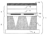
도 1은 본 발명의 신틸레이터 패널의 일실시형태를 구비하는 방사선 화상 검출 장치의 구성을 모식적으로 나타낸 단면도이다.
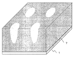
도 2는 본 발명의 신틸레이터 패널의 일실시형태의 구성을 모식적으로 나타낸 사시도이다.
도 3은 본 발명의 신틸레이터 패널의 일실시형태를 구비하는 방사선 화상 검출 장치의 구성을 모식적으로 나타낸 단면도이다.
도 4는 본 발명의 신틸레이터 패널의 일실시형태를 구비하는 방사선 화상 검출 장치의 구성을 모식적으로 나타낸 단면도이다.
도 5는 본 발명의 신틸레이터 패널의 일실시형태를 구비하는 방사선 화상 검출 장치의 구성을 모식적으로 나타낸 단면도이다.
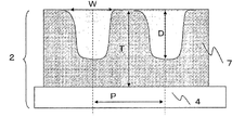
도 6은 본 발명의 신틸레이터 패널의 일실시형태의 구성을 모식적으로 나타낸 단면도이다.
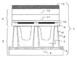
도 7은 격벽을 갖는 본 발명의 신틸레이터 패널의 일실시형태를 구비하는 방사선 화상 검출 장치의 구성을 모식적으로 나타낸 단면도이다.
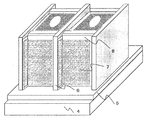
도 8은 격벽을 갖는 본 발명의 신틸레이터 패널의 일실시형태의 구성을 모식적으로 나타낸 사시도이다.
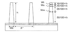
도 9는 격벽을 갖는 본 발명의 신틸레이터 패널의 일실시형태에 있어서의 격벽, 완충층 및 기판을 모식적으로 나타낸 단면도이다.
도 10은 격벽을 갖는 본 발명의 신틸레이터 패널의 일실시형태의 구성을 모식적으로 나타낸 단면도이다.BRIEF DESCRIPTION OF THE DRAWINGS Fig. 1 is a cross-sectional view schematically showing a configuration of a radiographic image detection apparatus including an embodiment of a scintillator panel according to the present invention. Fig.
2 is a perspective view schematically showing a configuration of an embodiment of a scintillator panel according to the present invention.
3 is a cross-sectional view schematically showing a configuration of a radiographic image detection apparatus including an embodiment of a scintillator panel according to the present invention.
4 is a cross-sectional view schematically showing a configuration of a radiographic image detection apparatus including an embodiment of a scintillator panel according to the present invention.
5 is a cross-sectional view that schematically shows a configuration of a radiographic image detection apparatus including an embodiment of a scintillator panel according to the present invention.
6 is a cross-sectional view schematically showing a configuration of an embodiment of a scintillator panel according to the present invention.
Fig. 7 is a cross-sectional view schematically showing a configuration of a radiographic image detection apparatus having an embodiment of a scintillator panel having a partition according to the present invention.
8 is a perspective view schematically showing a configuration of an embodiment of a scintillator panel according to the present invention having a partition wall.
9 is a cross-sectional view schematically showing a partition wall, a buffer layer and a substrate in an embodiment of the scintillator panel of the present invention having a partition wall.
10 is a cross-sectional view schematically showing a configuration of an embodiment of a scintillator panel according to the present invention having a partition wall.
본 발명의 신틸레이터 패널은 기판, 및 형광체 분말을 함유하는 형광체층을 구비하고, 상기 형광체층이 표면에 복수의 오목부를 갖고, 상기 오목부의 개구부의 면적(A)이 500~70000㎛2이며, 상기 형광체층의 두께(T)와, 상기 오목부의 깊이(D)의 비인 D/T가 0.1~0.9인 것을 특징으로 한다.A scintillator panel according to the present invention comprises a substrate and a phosphor layer containing a phosphor powder, wherein the phosphor layer has a plurality of recesses on its surface, the area (A) of the openings of the recesses is 500 to 70000 탆 2 , Wherein a ratio D / T of the thickness (T) of the phosphor layer to a depth (D) of the recess is 0.1 to 0.9.
이하에, 도면을 이용하여 본 발명의 신틸레이터 패널의 구체적인 구성 대해 설명하지만 본 발명은 이들에 의해 한정되는 것은 아니다. Hereinafter, the specific configuration of the scintillator panel of the present invention will be described with reference to the drawings, but the present invention is not limited thereto.
도 1, 3 내지 5 및 7은 본 발명의 신틸레이터 패널을 구비하는 방사선 화상 검출 장치의 구성을 모식적으로 나타낸 단면도이다. 도 2 및 8은 본 발명의 신틸레이터 패널의 구성을 모식적으로 나타낸 사시도이다. 방사선 화상 검출 장치(1)는 신틸레이터 패널(2), 검출 기판(3) 및 전원부(13)로 이루어진다.Figs. 1, 3 to 5 and 7 are cross-sectional views schematically showing the configuration of a radiographic image detection apparatus having a scintillator panel according to the present invention. Figs. 2 and 8 are perspective views schematically showing a configuration of a scintillator panel according to the present invention. The radiographic
신틸레이터 패널(2)은 기판(4), 및 기판(4) 상에 형성된 형광체 분말을 함유하는 형광체층(7)을 구비한다. 형광체층(7)은 표면에 복수의 오목부를 갖고 있다.The
검출 기판(3)은 기판(12) 상에 광전 변환 소자와 TFT로 이루어지는 화소가 2차원 형상으로 형성된 광전 변환층(10), 및 출력층(11)을 갖는다. 신틸레이터 패널(2)의 출광면과, 검출 기판(3)의 광전 변환층(10)을 접착층(9)을 통해 접착 또는 밀착시킴으로써 방사선 화상 검출 장치(1)가 구성된다. 이 때, 상기 광전 변환 소자의 화소와 상기 형광체층 표면의 1개 이상의 오목부가 대응하도록 한다. 하나의 화소에 1개의 오목부가 대응해도 상관없고, 하나의 화소에 2개 이상의 오목부가 대응해도 상관없다. 광전 변환 소자의 1화소에 대응하는 형광체층의 오목부의 수가 균일한 것이 바람직하다.The
방사선 화상 검출 장치(1)에 입사된 방사선은 형광체층(7)에 함유되는 형광체에 흡수되어서 가시광선이 방사된다. 이렇게 해서 형광체로부터 방사되는 광을 이하, 「형광체의 발광광」이라고 부른다. 광전 변환층(10)에 도달한 형광체의 발광광은 광전 변환층(10)에서 광전 변환되고, 출력층(11)을 통해 전기신호로서 출력된다.The radiation incident on the radiation
신틸레이터 패널의 기판의 재질로서는 예를 들면, 방사선의 투과성을 갖는 유리, 세라믹, 반도체, 고분자 화합물 또는 금속을 들 수 있다. 유리로서는 예를 들면 석영, 붕규산 유리 또는 화학적 강화 유리를 들 수 있다. 세라믹으로서는 예를 들면 사파이어, 질화규소 또는 탄화규소를 들 수 있다. 반도체로서는 예를 들면 실리콘, 게르마늄, 갈륨 비소, 갈륨 인 또는 갈륨 질소를 들 수 있다. 고분자 화합물로서는 예를 들면 셀룰로오스아세테이트, 폴리에스테르, 폴리아미드, 폴리이미드, 트리아세테이트, 폴리카보네이트 또는 탄소 섬유 강화 수지를 들 수 있다. 금속으로서는 예를 들면 알루미늄, 철, 구리 또는 금속 산화물을 들 수 있다.As a material of the substrate of the scintillator panel, for example, glass, ceramic, semiconductor, polymer compound or metal having radiation transmittance can be mentioned. Examples of the glass include quartz, borosilicate glass or chemically tempered glass. Examples of the ceramics include sapphire, silicon nitride, and silicon carbide. Examples of the semiconductor include silicon, germanium, gallium arsenide, gallium phosphorus and gallium nitrogen. Examples of the polymer compound include cellulose acetate, polyester, polyamide, polyimide, triacetate, polycarbonate or carbon fiber reinforced resin. Examples of metals include aluminum, iron, copper, and metal oxides.
또한, 신틸레이터 패널의 운반의 편리성의 점에서 신틸레이터 패널의 경량화가 진행되고 있는 점에서 기판 두께는 2.0㎜ 이하가 바람직하고, 1.0㎜ 이하가 보다 바람직하다. 또한, 형광체의 발광광을 고효율로 이용하기 위해서 반사율이 높은 기판이 바람직하다. 바람직한 기판의 재료로서는 유리 또는 고분자 화합물을 들 수 있다. 특히, 바람직한 예로서 고반사 폴리에스테르 기판을 들 수 있다. 고반사 폴리에스테르 기판으로서는 방사선의 투과성이 높고, 또한 저비중인 점에서 보이드를 포함하는 백색 폴리에스테르 기판이 더욱 바람직하다.The thickness of the substrate is preferably 2.0 mm or less, and more preferably 1.0 mm or less in view of the weight reduction of the scintillator panel from the viewpoint of convenience of transportation of the scintillator panel. Further, a substrate having a high reflectivity is preferable in order to utilize the emitted light of the phosphor with high efficiency. Preferable examples of the material of the substrate include glass or a polymer compound. In particular, a highly reflective polyester substrate is a preferable example. As a highly reflective polyester substrate, a white polyester substrate containing voids is more preferable because of high radiation transmittance and low specific gravity.
기판 상에 형광체층을 형성한다. 형광체층은 형광체 분말을 함유한다. 여기서 형광체 분말이란 평균 입자경(D50)이 40㎛ 이하인 형광체를 말한다. 형광체로서는 예를 들면 CsI, CsBr, Gd2O2S(이하, 「GOS」), Gd2SiO5, BiGe3O12, CaWO4, Lu2O2S, Y2O2S, LaCl3, LaBr3, LaI3, CeBr3, CeI3 또는 LuSiO5를 들 수 있다. 발광 효율을 높이기 위해서 형광체에 부활제를 첨가해도 상관없다. 부활제로서는 예를 들면 나트륨(Na), 인듐(In), 탈륨(Tl), 리튬(Li), 칼륨(K), 루비듐(Rb), 나트륨(Na), 테르븀(Tb), 세륨(Ce), 유로퓸(Eu) 또는 프라세오디뮴(Pr)을 들 수 있지만, 화학적 안정성이 높고, 또한 발광 효율이 높기 때문에 GOS에 Tb를 첨가한 Tb 부활 GOS(GOS:Tb)가 바람직하다.A phosphor layer is formed on the substrate. The phosphor layer contains a phosphor powder. Here, the phosphor powder means a phosphor having an average particle size (D50) of 40 占 퐉 or less. Examples of the fluorescent material include CsI, CsBr, Gd 2 O 2 S (hereinafter, "GOS"), Gd 2 SiO 5 , BiGe 3 O 12 , CaWO 4 , Lu 2 O 2 S, Y 2 O 2 S, LaCl 3 , LaBr 3, LaI 3, CeBr may be mentioned 3, CeI 3 or 5 LuSiO. An activator may be added to the phosphor in order to increase the luminous efficiency. Examples of the activator include sodium (Na), indium (In), thallium (Tl), lithium (Li), potassium (K), rubidium (Rb), sodium (Na), terbium (Tb) (Eu) or praseodymium (Pr). However, Tb-activated GOS (GOS: Tb) to which Tb is added to GOS is preferable because of its high chemical stability and high luminous efficiency.
형광체 분말은 구상, 편평상 또는 봉 형상 등인 것이 바람직하다. 형광체의 평균 입자경(D50)은 0.1~40㎛인 것이 바람직하고, 보다 바람직하게는 1.0~25㎛이며, 더 바람직하게는 1.0~20㎛이다. 한편, D50이 0.1㎛ 미만이면 형광체의 표면 결함에 의해 충분한 발광이 얻어지지 않는 경우가 있다. 또한, D50이 40㎛를 초과하면, 광전 변환 소자마다의 검출 강도의 변동이 크고, 선명한 화상이 얻어지지 않는 경우가 있다. The phosphor powder is preferably spherical, flat, or rod-shaped. The average particle diameter (D50) of the phosphor is preferably 0.1 to 40 占 퐉, more preferably 1.0 to 25 占 퐉, and still more preferably 1.0 to 20 占 퐉. On the other hand, if D50 is less than 0.1 mu m, sufficient light emission can not be obtained due to surface defects of the phosphor. When the D50 is more than 40 mu m, the variation of the detection intensity for each photoelectric conversion element is large, and a clear image may not be obtained.
형광체 분말의 평균 입자경(D50)은 입도 분포 측정 장치(예를 들면, MT3300; NIKKISO Co., Ltd. 제작)를 사용하여 물을 채운 시료실에 형광체 분말을 투입하고, 300초간 초음파 처리를 행한 후에 측정할 수 있다. The average particle size (D50) of the phosphor powder was measured by applying a phosphor powder to a sample chamber filled with water using a particle size distribution analyzer (for example, MT3300, manufactured by NIKKISO Co., Ltd.) and ultrasonic treatment for 300 seconds Can be measured.
형광체층은 그 표면에 복수의 오목부를 갖는다. 여기서 형광체층의 표면이란 형광체층에 있어서 기판과 반대측에 위치하는 면을 말한다. 형광체층이 갖는 오목부에 의해 형광체의 발광광을 거기에서 집광시킬 수 있고, 발광광의 산란을 억제하는 것이 가능해지기 때문에 보다 선명한 화상을 얻을 수 있다. 또한, 형광체층이 오목부를 가짐으로써 형광체의 발광광이 광전 변환층에 도달할 때까지의 형광체에 의한 광 흡수가 저감되어 발광광을 고효율로 이용할 수 있다.The phosphor layer has a plurality of recesses on its surface. Here, the surface of the phosphor layer means a surface located on the opposite side of the phosphor layer from the substrate. The light emitted from the phosphor can be condensed by the concave portion of the phosphor layer, and scattering of the emitted light can be suppressed, so that a clearer image can be obtained. In addition, since the phosphor layer has a concave portion, the light absorption by the phosphor until the emitted light of the phosphor reaches the photoelectric conversion layer is reduced, and the emitted light can be utilized with high efficiency.
형광체층이 갖는 오목부의 형상으로서는 예를 들면 도 1 또는 도 3 내지 5에 나타내는 것을 들 수 있다.Examples of the shape of the concave portion of the phosphor layer include those shown in Fig. 1 or Figs. 3 to 5.
형광체층의 오목부는 개구부의 면적(A)이 500~70000㎛2일 필요가 있다. 면적(A)이 500㎛2 미만이면 형광체의 발광광을 오목부에서 집광시킬 수 없어 발광광의 산란을 억제할 수 없다. 한편, 면적(A)이 70000㎛2를 초과하면 오목부가 광전 변환 소자의 화소 사이즈보다 커짐으로써 화소마다의 검출 광량에 불균일이 발생하기 때문에 선명한 화상이 얻어지지 않는다. The concave portion of the phosphor layer needs to have an opening area A of 500 to 70000 탆 2 . If the area A is less than 500 mu m < 2 >, the emitted light of the phosphor can not be focused in the concave portion, and scattering of the emitted light can not be suppressed. On the other hand, if the area A exceeds 70000 mu m < 2 & gt ;, the concave portion becomes larger than the pixel size of the photoelectric conversion element, the amount of detected light for each pixel is uneven, and a clear image can not be obtained.
면적(A)은 레이저 현미경(예를 들면, VK-9500; KEYENCE Corporation 제작) 을 사용하여 배율 20배로 기판에 대해서 수직 상방향으로부터 형광체층을 스캔한 화상을 해석해서 구할 수 있다. 보다 구체적으로는 스캔한 화상에 있어서 오목부를 무작위로 5점 선택하고, 각각의 개구부의 형상에 따라 면적을 구하기 때문에 수학적으로 필요한 길이(예를 들면, 개구부의 형상이 정원(正円)이면 그 직경; 개구부의 형상이 정사각형이면 한 변의 길이)를 측정해서 각 개구부의 면적을 구한 후에 5점의 평균값을 산출해서 구할 수 있다. The area A can be obtained by analyzing an image obtained by scanning a phosphor layer from a vertical upward direction with respect to a substrate at a magnification of 20 times using a laser microscope (for example, VK-9500, manufactured by KEYENCE Corporation). More specifically, five points are randomly selected from the concave portions in the scanned image, and the area is determined according to the shape of each opening. Therefore, when a mathematically necessary length (for example, (The length of one side when the shape of the opening is square), and calculating the average value of five points after determining the area of each opening.
도 6에 본 발명의 신틸레이터 패널의 일실시형태를 모식적으로 나타낸 단면도를 나타낸다. 신틸레이터 패널(2)에 있어서, 기판(4) 상에 두께(T)의 형광체층(7)이 형성되어 있다. 형광체층(7)은 표면에 복수의 오목부를 갖고 있다. 오목부의 개구부의 최대폭을 W, 깊이를 D로 한다. 또한, 서로 인접하는 오목부끼리의 간격을 피치(P)로 한다. 여기서, 인접하는 오목부끼리의 간격이란 어떤 오목부의 개구부의 중심점으로부터 인접하는 오목부의 중심점까지의 거리를 말한다.6 is a cross-sectional view schematically showing an embodiment of a scintillator panel according to the present invention. In the
오목부의 개구부의 최대폭(W)은 30~300㎛인 것이 바람직하고, 40~250㎛인 것이 보다 바람직하고, 40~150㎛인 것이 더욱 바람직하다. 개구부의 최대폭(W)이 30㎛ 미만이면, 오목부에 형광체의 발광광을 집광시킬 수 없어 발광광의 산란을 억제해서 선명한 화상을 얻을 수 없는 경우가 있다. 한편, 개구부의 최대폭(W)이 300㎛를 초과하면, 광전 변환 소자의 화소마다의 검출 광량의 불균일이 발생하기 때문에 선명한 화상이 얻어지지 않는 경우가 있다. The maximum width (W) of the opening of the concave portion is preferably 30 to 300 占 퐉, more preferably 40 to 250 占 퐉, and still more preferably 40 to 150 占 퐉. If the maximum width (W) of the opening is less than 30 mu m, the emitted light of the phosphor can not be focused on the concave portion, so that scattering of the emitted light can be suppressed and a clear image can not be obtained. On the other hand, if the maximum width (W) of the openings exceeds 300 mu m, the amount of detected light for each pixel of the photoelectric conversion element is uneven, so that a clear image may not be obtained.
오목부의 개구부의 최대폭(W)은 레이저 현미경(예를 들면, VK-9500; KEYENCE Corporation 제작)을 사용하여 배율 20배로 기판에 대해서 수직 상방으로부터 형광체층을 스캔한 화상을 해석해서 구할 수 있다. 보다 구체적으로는 스캔한 화상에 있어서 오목부를 무작위로 5점 선택하고, 각각의 개구부의 형상에 따른 수학적으로 필요한 길이(예를 들면, 개구부의 형상이 정원이면 그 직경; 개구부의 형상이 정사각형이면 그 대각선의 길이)에 대해서 5점의 평균값을 산출해서 구할 수 있다.The maximum width (W) of the opening of the concave portion can be obtained by analyzing an image obtained by scanning the phosphor layer from above and above with respect to the substrate at a magnification of 20 times using a laser microscope (for example, VK-9500; manufactured by KEYENCE Corporation). More specifically, five points of a concave portion are randomly selected in a scanned image, and a mathematically necessary length corresponding to the shape of each opening (for example, if the shape of the opening is large, the diameter thereof; if the shape of the opening is square, The length of the diagonal line), and calculating the average value of the five points.
형광체층의 두께(T)는 120~1000㎛가 바람직하고, 120~500㎛인 것이 보다 바람직하고, 120~350㎛인 것이 더욱 바람직하다. 형광체층의 두께(T)가 120㎛ 미만이면 방사선을 충분히 가시광선으로 변환할 수 없어 필요한 강도의 발광광이 얻어지지 않는 경우가 있다. 한편, 형광체 두께(T)가 1000㎛를 초과하면 방사선이 최선으로 조사되는 방사선의 조사 방향측에 존재하는 형광체의 강도가 높은 발광광이 광전 변환층까지 도달하지 않아 발광광을 고효율로 이용할 수 없는 경우가 있다. 다량의 형광체 분말이 더 필요해져 신틸레이터 패널의 비용이 증가되어 버린다. The thickness T of the phosphor layer is preferably 120 to 1000 占 퐉, more preferably 120 to 500 占 퐉, and even more preferably 120 to 350 占 퐉. If the thickness T of the phosphor layer is less than 120 mu m, the radiation can not be sufficiently converted into visible light, and the emitted light of necessary intensity may not be obtained. On the other hand, if the phosphor thickness (T) exceeds 1000 mu m, the luminescent light having a high intensity of the fluorescent material present on the irradiation side of the radiation in which the radiation is best irradiated does not reach the photoelectric conversion layer, There is a case. A larger amount of phosphor powder is required, which increases the cost of the scintillator panel.
형광체층의 두께(T)는 이하의 방법에 의해 측정할 수 있다. 우선, 형광체층을 무작위로 선택한 오목부가 없는 위치에서 기판에 대하여 수직방향으로 절단한다. 그 단면을 광학 현미경(예를 들면, OPTISHOT; NIKON CORPORATION 제작)을 사용하여 배율 20배로 관찰한 화상에 있어서 측정 위치를 무작위로 5점 선택하고, 각각의 측정 위치에 있어서의 형광체층의 높이를 측정한다. 이 조작을 5회 반복하고, 얻어진 높이의 값 모두(5×5)의 평균값을 형광체층의 두께(T)로 한다.The thickness (T) of the phosphor layer can be measured by the following method. First, the phosphor layer is cut in a direction perpendicular to the substrate at a position where the phosphor layer is not randomly selected. Five points of measurement positions are randomly selected in an image obtained by observing the cross section with an optical microscope (manufactured by OPTISHOT; NIKON CORPORATION, for example) at a magnification of 20, and the height of the phosphor layer at each measurement position is measured do. This operation is repeated five times, and the average value of all of the obtained height values (5 x 5) is taken as the thickness T of the phosphor layer.
형광체층의 오목부의 깊이(D)는 레이저 현미경(예를 들면, VK-9500; KEYENCE Corporation 제작)을 사용하여 배율 20배로 기판에 대해서 수직 상방향으로부터 형광체층을 스캔한 화상을 해석해서 구할 수 있다. 보다 구체적으로는 스캔한 화상에 있어서 오목부를 무작위로 5점 선택하고, 기판에 대하여 수직방향에 있어서의 각각의 개구부로부터 최심부까지의 거리의 평균값을 산출해서 오목부의 깊이(D)를 구할 수 있다.The depth D of the concave portion of the phosphor layer can be obtained by analyzing an image obtained by scanning the phosphor layer from the vertical upward direction with respect to the substrate at a magnification of 20 times using a laser microscope (for example, VK-9500, manufactured by KEYENCE Corporation) . More specifically, five points of the concave portions are randomly selected in the scanned image, and the depth D of the concave portion can be obtained by calculating the average value of the distances from the respective openings to the deepest portion in the direction perpendicular to the substrate .
형광체층의 두께(T)와 형광체층의 오목부의 깊이(D)의 비인 D/T는 0.1~0.9일 필요가 있지만 0.2~0.8인 것이 바람직하다. D/T가 0.1 미만이면 방사선을 충분히 가시광선으로 변환할 수 없어 필요한 강도의 발광광이 얻어지지 않는다. 또한, 오목부에서 집광된 형광체의 발광광이 기판측으로 누설되어 광전 변환층에 도달되지 않아 발광광의 이용 효율이 저하한다. 한편, D/T가 0.9를 초과하면 오목부에 형광체의 발광광을 집광시킬 수 없어 발광광의 산란을 억지해서 선명한 화상을 얻을 수 없다.D / T, which is the ratio of the thickness (T) of the phosphor layer and the depth (D) of the concave portion of the phosphor layer, is preferably 0.1 to 0.9, but is preferably 0.2 to 0.8. If the D / T is less than 0.1, the radiation can not be sufficiently converted into visible light, and the emitted light of the required intensity can not be obtained. Further, the light emitted from the phosphor condensed in the concave portion leaks to the substrate side and does not reach the photoelectric conversion layer, and the use efficiency of the emitted light decreases. On the other hand, if the D / T ratio exceeds 0.9, the emitted light of the phosphor can not be focused on the concave portion, so that scattering of the emitted light is inhibited and a clear image can not be obtained.
형광체층은 표면에 500~50000개/㎠의 오목부를 갖는 것이 바람직하고, 또한 1200~15000개/㎠의 오목부를 갖는 것이 보다 바람직하다. 오목부의 수가 500개/㎠ 미만이면 광전 변환 소자의 1화소에 대응하는 형광체층의 오목부의 수의 불균일이 커져 선명한 화상을 얻을 수 없는 경우가 있다. 한편, 오목부의 수가 50000개/㎠를 초과하면 오목부에서 형광체의 발광광을 집광시킬 수 없고, 또한 형광체 분말의 양이 저하하기 때문에 필요한 강도의 발광광이 얻어지지 않는 경우가 있다. It is preferable that the phosphor layer has a concave portion of 500 to 50000 /
형광체층이 갖는 오목부의 수는 광학 현미경(예를 들면, OPTISHOT; NIKON CORPORATION 제작)을 사용하여 배율 20배로 기판에 대해서 수직 상방향으로부터 형광체층을 스캔한 화상을 해석해서 구할 수 있다. 보다 구체적으로는 스캔한 화상에 있어서 무작위로 10개소 선택한 1㎟의 영역에 있어서의 오목부의 수를 각각 측정하고, 그 평균값을 1㎠당 값으로 변환해서 구할 수 있다.The number of the recesses of the phosphor layer can be obtained by analyzing an image obtained by scanning the phosphor layer from the vertical upward direction with respect to the substrate at a magnification of 20 times using an optical microscope (manufactured by OPTISHOT; manufactured by NIKON CORPORATION). More specifically, it is possible to measure the number of recesses in a region of 1
서로 인접하는 오목부끼리의 피치(P)는 대응하는 광전 변환 소자의 피치에 따라 적당히 변경하면 좋지만 50~350㎛의 범위가 바람직하고, 50~280㎛의 범위가 보다 바람직하다. 또한, 인접하는 오목부끼리의 피치(P)는 상기 범위 내에 있어서의 일정값인 것이 바람직하다. 즉, 형광체층이 갖는 오목부는 광전 변환 소자의 1화소당 대응하는 오목부의 수를 균일하게 하기 위해서 50~350㎛의 범위에 있어서의 일정값으로 등간격으로 배치되어 있는 것이 바람직하다. 피치(P)가 50㎛ 미만이면 오목부에서 형광체의 발광광을 집광할 수 없는 경우가 있다. 한편, 피치(P)가 350㎛를 초과하면 광전 변환 소자의 1화소당 1개 이상의 오목부를 대응시키는 것이 곤란해지는 경우가 있다. 피치(P)는 50~280㎛의 범위에 있어서의 일정값인 것이 보다 바람직하다.The pitch P between adjacent concave portions may be appropriately changed in accordance with the pitch of the corresponding photoelectric conversion element, but is preferably in the range of 50 to 350 mu m, more preferably in the range of 50 to 280 mu m. It is preferable that the pitch P between adjacent concave portions is a constant value within the above range. That is, it is preferable that the concave portion of the phosphor layer is arranged at regular intervals in a range of 50 to 350 占 퐉 in order to make the number of concave portions corresponding to one pixel of the photoelectric conversion element uniform. If the pitch P is less than 50 占 퐉, the emitted light of the phosphor can not be condensed in the concave portion. On the other hand, when the pitch P exceeds 350 mu m, it may be difficult to correspond one or more concave portions per pixel of the photoelectric conversion element. It is more preferable that the pitch P is a constant value in the range of 50 to 280 mu m.
서로 인접하는 오목부끼리의 피치(P)는 레이저 현미경(예를 들면, VK-9500; KEYENCE Corporation 제작)을 사용하여 배율 20배로 기판에 대해 수직 상방향으로 부터 형광체층을 스캔한 화상을 해석해서 구할 수 있다. 보다 구체적으로는 스캔한 화상에 있어서 오목부의 개구부의 중심점으로부터 인접하는 오목부의 중심점까지의 거리를 무작위로 10점 측정하고, 그 평균값을 산출해서 오목부의 피치(P)로 한다.The pitch P between adjacent concave portions is obtained by interpolating an image obtained by scanning the phosphor layer from the vertical upward direction with respect to the substrate at a magnification of 20 times using a laser microscope (for example, VK-9500 manufactured by KEYENCE Corporation) Can be obtained. More specifically, in the scanned image, the distance from the center point of the opening of the recess to the center point of the adjacent recess is randomly measured at 10 points, and the average value is calculated to be the pitch (P) of the recess.
형광체층이 갖는 오목부의 형상은 기판에 대해서 수평방향의 오목부의 단면의 면적이 개구부에 있어서 최대이며, 오목부의 깊이(D)가 커져도 그 수평방향의 면적이 변화하지 않거나, 또는 깊이(D)가 커짐에 따라 그 수평방향의 면적이 작아지는 형상인 것이 바람직하다. 형광체층이 갖는 오목부의 형상은 개구부를 저면으로 하는 대략 원추 형상 등이 바람직하다. 여기서, 대략 원추 형상의 「대략 」이란 오목부의 형상이 엄밀한 의미에서의 원추일 필요는 없고 저면(오목부의 개구부 형상)이 타원이거나, 정점(오목부의 최심부 형상)이 도 2에 나타낸 바와 같이 둥그스름해 있거나 해도 상관없는 것을 의미한다. 오목부가 그러한 형상인 것에 의해 오목부에서 집광된 발광광을 오목부의 내부에 가두는 일 없이 발광광을 고효율로 이용할 수 있다. The shape of the concave portion of the phosphor layer is the largest in the cross section of the concave portion in the horizontal direction with respect to the substrate and the area in the horizontal direction does not change even if the depth D of the concave portion is large, It is preferable that the shape is such that the area in the horizontal direction becomes smaller as the size increases. The shape of the concave portion of the phosphor layer is preferably a substantially conical shape with the opening portion as the bottom surface. Here, the " roughly " of the substantially conical shape does not necessarily mean that the shape of the concave portion is a cone in a strict sense, and the shape of the bottom surface (the shape of the opening of the concave portion) is an ellipse, or the vertex (the deepest portion of the concave portion) It means that it does not matter whether it is done or not. Since the concave portion has such a shape, the emitted light can be used with high efficiency without blocking the light-emitting light condensed in the concave portion inside the concave portion.
기판 상에 형광체층을 형성하는 방법으로서는 기판 상에 형광체 분말을 함유하는 페이스트, 즉 형광체 페이스트를 도포해서 도포막을 형성하는 방법을 들 수 있다. 이렇게 해서 얻어진 형광체 페이스트의 도포막에 오목부를 형성함으로써 표면에 복수의 오목부를 갖는 형광체층을 얻을 수 있다. 도포막을 얻기 위한 형광체 페이스트의 도포 방법으로서는 예를 들면 스크린 인쇄법, 바 코터, 롤 코터, 다이 코터 또는 블레이드 코터를 들 수 있다. As a method of forming a phosphor layer on a substrate, there is a method of forming a coating film by applying a paste containing a phosphor powder, that is, a phosphor paste, on a substrate. By forming the concave portion in the coating film of the phosphor paste thus obtained, a phosphor layer having a plurality of concave portions on the surface can be obtained. Examples of the application method of the phosphor paste for obtaining the coating film include a screen printing method, a bar coater, a roll coater, a die coater or a blade coater.
형광체 페이스트는 유기 바인더를 함유해도 상관없다. 유기 바인더로서는 예를 들면 폴리비닐부티랄, 폴리비닐아세테이트, 폴리비닐알코올, 에틸셀룰로오스, 메틸셀룰로오스, 폴리에틸렌, 폴리메틸실록산 또는 폴리메틸페닐실록산 등의 실리콘 수지, 폴리스티렌, 부타디엔/스티렌 코폴리머, 폴리스티렌, 폴리비닐피롤리돈, 폴리아미드, 고분자량 폴리에테르, 에틸렌옥사이드와 프로필렌옥사이드의 공중합체, 폴리아크릴아미드 또는 아크릴수지를 들 수 있다.The phosphor paste may contain an organic binder. Examples of the organic binder include silicone resins such as polyvinyl butyral, polyvinyl acetate, polyvinyl alcohol, ethyl cellulose, methylcellulose, polyethylene, polymethylsiloxane or polymethylphenylsiloxane, polystyrene, butadiene / styrene copolymer, polystyrene, poly Vinyl pyrrolidone, polyamide, high molecular weight polyether, copolymer of ethylene oxide and propylene oxide, polyacrylamide or acrylic resin.
형광체 페이스트는 유기용매를 함유해도 상관없다. 형광체 페이스트가 유기 바인더를 함유하는 경우, 유기용매는 그 양용매이며, 수소 결합력이 큰 것이 바람직하다. 그러한 유기용매로서는 예를 들면 디에틸렌글리콜모노부틸에테르아세테이트, 에틸렌글리콜모노부틸에테르알코올, 디에틸렌글리콜모노부틸에테르, 메틸에틸케톤, 시클로헥산온, 이소부틸알코올, 이소프로필알코올, 테르피넨올, 벤질알코올, 테트라히드로푸란, 디메틸술폭시드, 디히드로터피넨올, γ-부티로락톤, 디히드로테르피닐아세테이트, 3-메톡시-3-메틸-메틸부탄올, 프로필렌글리콜모노메틸에테르, 프로필렌글리콜모노메틸에테르아세테이트, N,N-디메틸포름아미드, 헥실렌글리콜 또는 브로모벤조산을 들 수 있다.The phosphor paste may contain an organic solvent. When the phosphor paste contains an organic binder, the organic solvent is a good solvent and preferably has a high hydrogen bonding force. Examples of such an organic solvent include diethylene glycol monobutyl ether acetate, ethylene glycol monobutyl ether alcohol, diethylene glycol monobutyl ether, methyl ethyl ketone, cyclohexanone, isobutyl alcohol, isopropyl alcohol, terpinenol, benzyl But are not limited to, alcohol, tetrahydrofuran, dimethylsulfoxide, dihydrotopheneol,? -Butyrolactone, dihydroterpinylacetate, 3-methoxy-3-methyl-methylbutanol, propylene glycol monomethyl ether, propylene glycol monomethyl Ether acetate, N, N-dimethylformamide, hexylene glycol or bromobenzoic acid.
형광체 페이스트는 그 점도를 조정하기 위해서 증점제, 가소제 또는 침강 방지제를 함유해도 상관없다. The phosphor paste may contain a thickener, a plasticizer or an anti-settling agent in order to adjust its viscosity.
형광체 페이스트의 도포막에 오목부를 형성하는 방법으로서는 예를 들면 에칭법, 금형 프레스법, 샌드 블라스트법, 감광성 페이스트법 등을 들 수 있다. 특히, 오목부에 대응하는 볼록형의 패턴을 형성한 금형을 프레스기를 사용하여 형광체 페이스트 도포막에 압입하는 방법이 공정수가 적고, 형광체 페이스트 재료의 선택성이 높고, 오목부를 형성한 후의 형광체 페이스트 도포막에의 불순물의 혼입을 억제할 수 있기 때문에 바람직하다. 금형의 재료는 금속이어도, 세라믹이어도, 수지이어도 좋지만 투명 또는 백색의 세라믹이 바람직하다. 또한, 금형에 형성되는 볼록형의 패턴은 상기한 바와 같이 오목부에 대응하는 것이므로 목적으로 하는 오목부의 형상 및 피치에 맞춰 형성한다. 구체적으로는 상기 바람직한 오목부의 형상 및 피치에 맞춰 금형의 볼록형 패턴을 형성하는 것이 바람직하다.Examples of the method for forming the concave portion in the coating film of the phosphor paste include an etching method, a mold press method, a sand blast method, and a photosensitive paste method. Particularly, a method of press-inserting a metal mold having a convex pattern corresponding to the concave portion into the phosphor paste coating film by using a press machine is advantageous in that the number of steps is small and the selectivity of the phosphor paste material is high, and the phosphor paste coating film It is possible to suppress the incorporation of impurities in the film. The material of the mold may be a metal, a ceramic, a resin, or a transparent or white ceramic. Since the convex pattern formed on the metal mold corresponds to the concave portion as described above, it is formed in conformity with the shape and pitch of the desired concave portion. Specifically, it is preferable to form the convex pattern of the mold in conformity with the shape and pitch of the preferable concave portion.
구체적으로는 형광체 페이스트 도포막 상에 볼록형 패턴을 형성한 금형을 0.1~100MPa로 프레스하는 것이 바람직하고, 0.3~10MPa로 프레스하는 것이 보다 바람직하다. 또한, 금형으로 프레스할 때에 25~200℃로 가열함으로써 바람직하게 형광체 페이스트 도포막에 오목부를 형성할 수 있다.Concretely, it is preferable to press the mold having the convex pattern formed on the phosphor paste coating film at a pressure of 0.1 to 100 MPa, more preferably 0.3 to 10 MPa. Further, when pressed by a mold, it is possible to form a concave portion in the phosphor paste coating film preferably by heating to 25 to 200 캜.
신틸레이터 패널은 형광체층을 복수의 셀로 구획하는 격벽을 더 갖는 것이 바람직하다.The scintillator panel preferably further includes a partition wall partitioning the phosphor layer into a plurality of cells.
도 7은 격벽을 갖는 실시형태의 신틸레이터 패널을 구비하는 방사선 화상 검출 장치의 구성을 모식적으로 나타낸 단면도이다. 도 7에 나타내는 신틸레이터 패널(2)은 기판(4), 기판(4) 상에 재치된 격벽(6), 및 격벽(6)에 의해 복수의 셀로 구획된 형광체층(7)을 구비한다. 형광체층(7)은 역시 복수의 오목부를 갖고 있다.7 is a cross-sectional view schematically showing the configuration of a radiation image detecting apparatus having a scintillator panel according to an embodiment having a partition. The
기판(4)과 격벽(6) 사이에는 완충층(5)이 형성되어 있는 것이 바람직하다. 완충층(5)을 형성함으로써 격벽(6)의 안정적인 형성이 가능해진다. 또한, 이 완충층(5)의 가시광선에 대한 반사율을 높게 함으로써 형광체층(7)이 함유하는 형광체 분말의 발광광을 고효율로 검출 기판(3) 상의 광전 변환층(10)에 도달시킬 수 있다.It is preferable that a
또한, 격벽(6)에 의해 구획된 각 셀 내에 반사율이 높은 반사층(8)을 형성함으로써 형광체층(7)이 함유하는 형광체 분말의 발광광을 고효율로 검출 기판(3)의 광전 변환층(10)에 도달시킬 수 있다.The
형광체층은 격벽에 의해 구획되어 있으므로 검출 기판(3)에 격자 형상으로 배치된 광전 변환 소자의 화소의 크기 및 피치와, 신틸레이터 패널(2)의 격벽에 의해 구획된 셀의 크기 및 피치를 대응시켜서 광전 변환층(10)에 있어서의 광전 변환 소자를 배치함으로써 형광체의 발광광의 산란이 인접하는 셀에 영향을 주는 것을 방지할 수 있다. Since the phosphor layers are partitioned by the partition walls, the size and pitch of the pixels of the photoelectric conversion elements arranged in a lattice pattern on the
격벽의 높이(h)는 120~1000㎛인 것이 바람직하고, 160~500㎛인 것이 보다 바람직하다. 높이(h)가 1000㎛를 초과하면 격벽 형성이 곤란해지는 경우가 있다. 한편, 높이(h)가 120㎛ 미만이면 형광체 분말의 양이 저하하기 때문에 필요한 강도의 발광광이 얻어지지 않는 경우가 있다. The height h of the partition wall is preferably 120 to 1000 mu m, more preferably 160 to 500 mu m. If the height h exceeds 1000 mu m, it may be difficult to form the barrier ribs. On the other hand, if the height h is less than 120 탆, the amount of the phosphor powder is lowered, so that the luminescent light of the required intensity may not be obtained.
격벽의 형상은 검출 기판이 구비하는 광전 변환 소자의 화소의 형상에 맞춰 적당히 선택하면 좋지만 도 8에 나타내는 바와 같은 격자 형상이 바람직하다. 격자 형상으로 구획된 셀의 개구부의 형상으로서는 예를 들면 정사각형, 직사각형, 평행사변형 또는 사다리꼴을 들 수 있지만, 발광광의 강도가 보다 균질해지는 점에서 정사각형이 바람직하다. The shape of the barrier rib may be suitably selected in accordance with the shape of the pixel of the photoelectric conversion element of the detection substrate, but it is preferable that the shape of the partition is a lattice shape as shown in Fig. The shape of the opening of the cell partitioned into the lattice shape may be, for example, a square, a rectangle, a parallelogram, or a trapezoid, but a square is preferable in that the intensity of the emitted light becomes more uniform.
격자 형상의 격벽에 있어서 서로 인접하는 격벽 간의 거리인 피치(P')는 50~1000㎛인 것이 바람직하다. 피치(P')가 50㎛ 미만이면, 격벽 형성이 곤란해지는 경우가 있다. 한편, 피치(P')가 1000㎛를 초과하면 선명한 화상이 얻어지지 않는 경우가 있다. It is preferable that the pitch P ', which is the distance between adjacent barrier ribs in the lattice-shaped barrier rib, is 50 to 1000 μm. If the pitch P 'is less than 50 탆, it may be difficult to form the barrier ribs. On the other hand, if the pitch P 'exceeds 1000 mu m, a clear image may not be obtained.
격벽의 저부의 폭(Wb)은 15~150㎛인 것이 바람직하다. 격벽의 50% 높이 위치의 폭(Wm)은 15~120㎛인 것이 바람직하다. 격벽의 75% 높이 위치의 폭(Ws) 및 격벽의 정부 폭(Wt)은 80㎛ 이하인 것이 바람직하다. 폭(Wb) 및 폭(Wm)이 15㎛ 미만이면 격벽의 결손 등이 생기기 쉽다. 한편, 폭(Wb)이 150㎛를 초과하거나, 또는 폭(Wm)이 120㎛를 초과하면 형광체 분말의 양이 저하하기 때문에 필요한 강도의 발광광이 얻어지지 않는 경우가 있다. 폭(Ws) 및 폭(Wt)이 80㎛를 초과하면 형광체의 발광광의 진행이 저해되어서 광전 변환층에 도달하지 않아 발광광의 이용 효율이 저하하는 경우가 있다. 또한, 폭(Wb)이란 도 9에 나타내는 바와 같이 격벽을 그 높이방향으로, 또한 길이방향으로 수직으로 절단했을 때의 단면에 있어서의 격벽과, 기판 또는 완충층이 접하는 위치에 있어서의 격벽의 폭을 말한다. 여기서, 격자 형상의 격벽에 있어서는 피치(P')의 반분 위치에 있어서 절단한다. 또한, 폭(Wm)이란 동 단면에 있어서의 높이가 격벽의 높이(h)의 50%의 위치에 있어서의 격벽의 폭을 말한다. 폭(Ws)이란 동 단면에 있어서의 높이가 격벽의 높이(h)의 75%의 위치에 있어서의 격벽의 폭을 말한다. 폭(Wt)이란 동 단면에 있어서의 높이가 격벽의 높이(h)의 90%의 위치에 있어서의 격벽의 폭을 말한다. 높이(h), 폭(Wb), 폭(Wm), 폭(Ws) 및 폭(Wt)은 격벽의 단면을 SEM으로 관찰해서 3개소 이상 측정하고, 그들의 평균값을 산출해서 구할 수 있다. 또한, 격벽의 단면은 형광체의 발광광을 효율적으로 광전 변환층에 도달시키기 위해서 격벽의 저부로부터 정부를 향해 그 폭이 감쇠하는 형상, 즉 도 7 및 도 9 에 나타내는 바와 같은 테이퍼 형상인 것이 바람직하다.The width Wb of the bottom of the barrier rib is preferably 15 to 150 mu m. It is preferable that the width (Wm) of the 50% height position of the barrier rib is 15 to 120 占 퐉. It is preferable that the width Ws of the partition wall at a 75% height position and the width Wt of the partition wall are 80 탆 or less. If the width (Wb) and the width (Wm) are less than 15 占 퐉, the partition wall tends to be defective. On the other hand, when the width Wb exceeds 150 占 퐉 or the width Wm exceeds 120 占 퐉, the amount of the phosphor powder decreases, so that the luminescent light of necessary intensity may not be obtained. If the width Ws and the width Wt exceed 80 mu m, the progress of the emitted light of the phosphor is inhibited and the light does not reach the photoelectric conversion layer, and the efficiency of utilization of the emitted light may be lowered. As shown in Fig. 9, the width Wb is defined as the width of the partition wall at the position where the partition wall contacts the substrate or the buffer layer when the partition wall is cut vertically in the height direction and perpendicularly to the longitudinal direction It says. Here, the lattice-shaped partitions are cut at half the pitch P '. The width Wm means the width of the partition at the position of 50% of the height h of the partition wall in the cross section. The width Ws is the width of the partition at the position of 75% of the height h of the partition wall in the cross section. The width Wt is the width of the partition at the position of 90% of the height h of the partition wall in the cross section. The height h, the width Wb, the width Wm, the width Ws and the width Wt can be obtained by measuring the cross-section of the partition at three or more positions by observing with SEM and calculating the average value thereof. It is also preferable that the cross section of the barrier rib is a shape in which the width of the barrier rib is attenuated from the bottom of the barrier rib toward the top of the barrier rib so as to efficiently reach the photoelectric conversion layer, that is, the taper shape as shown in Figs. 7 and 9 .
격벽의 재질로서는 예를 들면 아크릴계 수지, 폴리에스테르계 수지 또는 에폭시계 수지 등의 수지, 유리 또는 금속을 들 수 있다. 생산성 및 기계적 강도의 관점으로부터 유리를 주성분으로 하는 것이 바람직하다. 여기서, 유리를 주성분으로 한다란 격벽에 차지하는 유리의 비율이 60질량% 이상인 것을 말한다. 상기 비율은 70질량% 이상인 것이 보다 바람직하다.Examples of the material of the barrier rib include resins such as acrylic resin, polyester resin or epoxy resin, glass or metal. From the viewpoint of productivity and mechanical strength, it is preferable to use glass as a main component. Here, the term " made mainly of glass " means that the proportion of the glass in the partition wall is 60% by mass or more. The above ratio is more preferably 70% by mass or more.
격벽을 형성하는 방법으로서는 예를 들면 에칭법, 스크린 인쇄법, 샌드 블라스트법, 금형 전사법 또는 감광성 페이스트법을 들 수 있다. 고선명의 격벽을 얻기 위해서 감광성 페이스트법이 바람직하다.Examples of the method of forming the barrier ribs include etching, screen printing, sandblasting, die transfer, or photosensitive paste. A photosensitive paste method is preferable in order to obtain a high-definition barrier rib.
감광성 페이스트법이란 기판 상에 감광성 유기 성분을 함유하는 감광성 페이스트를 도포하고, 감광성 페이스트 도포막을 형성하는 도포 공정과, 얻어진 감광성 페이스트 도포막을 소망의 개구부를 갖는 포토마스크를 통해 노광하는 노광 공정과, 노광 후의 감광성 페이스트 도포막의 현상액에 가용된 부분을 용해 제거하는 현상 공정을 구비하는 격벽의 형성 방법을 말한다.The photosensitive paste method refers to a coating process of applying a photosensitive paste containing a photosensitive organic component on a substrate to form a photosensitive paste coating film, an exposure process of exposing the obtained photosensitive paste coating film through a photomask having a desired opening, And a developing step of dissolving and removing a portion of the photosensitive paste coating film that is later used in the developing solution.
또한, 상기 감광성 페이스트 내에 저융점 유리 분말을 함유하게 하고, 현상 공정 후의 감광성 페이스트 패턴을 고온으로 가열해서 유기 성분을 분해 증류 제거 함과 아울러 저융점 유리를 연화 및 소결시켜 격벽을 형성하는 소성 공정을 더 구비하는 것도 바람직하다. Further, the photosensitive paste containing the low melting point glass powder in the photosensitive paste, heating the photosensitive paste pattern after the development step to a high temperature to decompose and remove the organic components, and a sintering step of softening and sintering the low melting point glass to form the partition walls It is also preferable to further include the above.
소성 공정에 있어서의 가열 온도는 500~700℃가 바람직하고, 500~650℃가 보다 바람직하다. 가열 온도가 500℃ 이상이면 유기 성분이 완전히 분해 증류 제거됨과 아울러 저융점 유리 분말이 연화 및 소결된다. 한편, 가열 온도가 700℃를 초과하면 기판 등의 변형이 커지는 경우가 있다. The heating temperature in the firing step is preferably 500 to 700 占 폚, more preferably 500 to 650 占 폚. When the heating temperature is 500 ° C or higher, the organic component is completely decomposed and removed, and the low melting point glass powder is softened and sintered. On the other hand, if the heating temperature exceeds 700 ° C, the deformation of the substrate or the like may become large.
감광성 페이스트는 유기 성분과 무기 분말을 함유하는 것이 바람직하다. 감광성 페이스트에 차지하는 무기 분말의 비율은 30~80질량%가 바람직하고, 40~70질량%가 보다 바람직하다. 무기 분말의 비율이 30질량% 미만이면 즉 유기 성분이 과다이면 소성 공정에 있어서의 수축률이 커지고, 격벽의 결손이 생기기 쉽다. 한편, 무기 분말의 함유량이 80질량%를 초과하면, 즉 유기 성분이 과소이면 감광성 페이스트의 안정성이나 도포성에 악영향을 미칠 뿐만 아니라 무기 분말의 분산성이 저하되어 격벽의 결손이 생기기 쉽다. 또한, 무기 분말에 차지하는 저융점 유리 분말의 비율은 50~100질량%가 바람직하다. 저융점 유리 분말의 비율이 50질량% 미만이면 소결이 불충분해지고, 격벽의 강도가 저하하는 경우가 있다.The photosensitive paste preferably contains an organic component and an inorganic powder. The ratio of the inorganic powder to the photosensitive paste is preferably 30 to 80 mass%, more preferably 40 to 70 mass%. If the ratio of the inorganic powder is less than 30 mass%, that is, if the organic component is excessive, the shrinkage ratio in the firing step becomes large, and the defect of the partition easily tends to occur. On the other hand, if the content of the inorganic powder is more than 80% by mass, that is, if the organic component is too small, the stability and coating properties of the photosensitive paste are adversely affected, and the dispersibility of the inorganic powder is lowered. The ratio of the low melting point glass powder to the inorganic powder is preferably 50 to 100% by mass. When the proportion of the low melting point glass powder is less than 50 mass%, sintering becomes insufficient and the strength of the partition wall may be lowered.
저융점 유리 분말의 연화 온도는 480℃ 이상이 바람직하다. 연화 온도가 480℃ 미만이면 유기 성분이 분해 증류 제거되지 않은 채 유리 중에 잔존해버려 착색 등의 원인이 되는 경우가 있다. 소성 공정에 있어서의 가열 온도를 고려하면 저융점 유리의 연화 온도는 480~700℃가 바람직하고, 480~640℃가 보다 바람직하고, 480~620℃가 더욱 바람직하다.The softening temperature of the low melting point glass powder is preferably 480 DEG C or higher. If the softening temperature is lower than 480 占 폚, the organic component may remain in the glass without being subjected to decomposition distillation removal, resulting in coloring or the like. Considering the heating temperature in the firing step, the softening temperature of the low melting point glass is preferably 480 to 700 占 폚, more preferably 480 to 640 占 폚, and still more preferably 480 to 620 占 폚.
저융점 유리의 연화 온도는 시차 열 분석 장치(예를 들면, 차동형 시차 열 천칭 TG8120; Rigaku Corporation 제작)를 사용하여 샘플을 측정해서 얻어지는 DTA 곡선으로부터 흡열 피크에 있어서의 흡열 종료 온도를 접선법에 의해 외삽해서 산출할 수 있다. 보다 구체적으로는 알루미나 분말을 표준 시료로서 시차 열 분석 장치를 실온으로부터 20℃/분으로 승온시켜서 측정 샘플이 되는 저융점 유리 분말을 측정하여 DTA 곡선을 얻는다. 얻어진 DTA 곡선으로부터 흡열 피크에 있어서의 흡열 종료 온도를 접선법에 의해 외삽해서 구한 연화점(Ts)을 저융점 유리의 연화 온도로 할 수 있다.The softening temperature of the low melting point glass is determined by the tangential method from the DTA curve obtained by measuring the sample using a differential thermal analyzer (for example, differential differential thermal balance TG8120; manufactured by Rigaku Corporation) Can be extrapolated. More specifically, the alumina powder is heated as a standard sample from a room temperature to 20 DEG C / min to measure a low melting point glass powder as a measurement sample to obtain a DTA curve. From the obtained DTA curve, the softening point Ts obtained by extrapolating the endothermic end temperature in the endothermic peak by the tangential method can be set as the softening temperature of the low melting glass.
저융점 유리의 열팽창계수는 40~90×10-7(/K)가 바람직하다. 열팽창계수가 90×10-7(/K)를 초과하면 얻어지는 신틸레이터 패널의 휨이 커지고, 발광광의 크로스토크 등에 의해 화상의 선명도가 저하하는 경우가 있다. 한편, 열팽창계수가 40×10-7(/K) 미만이면 저융점 유리의 연화 온도가 충분히 낮아지지 않는 경우가 있다. The coefficient of thermal expansion of the low-melting glass is preferably from 40 to 90 x 10 < -7 > (/ K). If the coefficient of thermal expansion exceeds 90 占10-7 (/ K), the warp of the obtained scintillator panel becomes large, and the sharpness of the image may be lowered due to crosstalk of the emitted light. On the other hand, when the thermal expansion coefficient is less than 40 x 10 < -7 > (/ K), the softening temperature of the low melting point glass may not be sufficiently lowered.
유리를 저융점화하기 위한 함유 성분으로서는 예를 들면 산화납, 산화비스무트, 산화아연 또는 알칼리 금속 산화물을 들 수 있다. 산화리튬, 산화나트륨 및 산화칼륨으로 이루어지는 군으로부터 선택되는 알칼리 금속 산화물의 함유 비율에 따라 저융점 유리의 연화 온도를 조정하는 것이 바람직하다.Examples of the component for lowering the melting point of the glass include lead oxide, bismuth oxide, zinc oxide and alkali metal oxides. It is preferable to adjust the softening temperature of the low melting point glass in accordance with the content of the alkali metal oxide selected from the group consisting of lithium oxide, sodium oxide and potassium oxide.
저융점 유리에 차지하는 알칼리 금속 산화물의 비율은 2~20질량%로 하는 것이 바람직하다. 알칼리 금속 산화물의 비율이 2질량% 미만이면 저융점 유리의 연화 온도가 높아져서 소성 공정에서 고온에서의 가열이 필요해지고, 기판에 변형이 생기거나, 격벽에 결손이 생기거나 하기 쉽다. 한편, 알칼리 금속 산화물의 비율이 20질량%를 초과하면 소성 공정에 있어서 저융점 유리의 점도가 과도하게 저하하고, 얻어지는 격벽의 형상에 변형이 생기기 쉽다. 또한, 얻어지는 격벽의 공극률이 과도하게 작아지고, 얻어지는 신틸레이 패널에서 필요한 강도의 발광광이 얻어지지 않는다. The proportion of the alkali metal oxide in the low-melting glass is preferably 2 to 20% by mass. If the proportion of the alkali metal oxide is less than 2% by mass, the softening temperature of the low melting point glass becomes high and heating at a high temperature is required in the firing step, and the substrate is likely to deform or a defect is likely to occur in the partition wall. On the other hand, if the proportion of the alkali metal oxide exceeds 20 mass%, the viscosity of the low melting point glass is excessively lowered in the sintering step, and the shape of the obtained barrier is liable to be deformed. In addition, the porosity of the obtained barrier ribs becomes excessively small, and the emitted light of the required intensity can not be obtained in the resulting sintil ray panel.
저융점 유리는 알칼리 금속 산화물에 추가하여 고온에서의 점도의 조정을 위해 산화아연을 3~10질량% 함유하는 것이 바람직하다. 산화아연의 비율이 3질량% 미만이면 저융점 유리의 고온에서의 점도가 과도하게 높아진다. 한편, 산화아연의 비율이 10질량%를 초과하면 저융점 유리의 비용이 상승한다. The low melting point glass preferably contains 3 to 10 mass% of zinc oxide for adjusting the viscosity at high temperature in addition to the alkali metal oxide. If the proportion of zinc oxide is less than 3 mass%, the viscosity of the low-melting glass at high temperature becomes excessively high. On the other hand, if the proportion of zinc oxide exceeds 10% by mass, the cost of the low-melting glass increases.
또한, 저융점 유리는 상기 알칼리 금속 산화물 및 산화아연에 추가하여 산화규소, 산화붕소, 산화알루미늄 및 알칼리 토류 금속의 산화물 등을 함유시킴으로써 저융점 유리의 안정성, 결정성, 투명성, 굴절률 및 열팽창 특성 등을 조정하는 것이 가능하다. 알칼리 토류 금속의 산화물로서는 마그네슘, 칼슘, 바륨 및 스트론튬으로 이루어지는 군으로부터 선택되는 산화물을 함유하는 것이 바람직하다.In addition, the low-melting glass contains the oxides of silicon oxide, boron oxide, aluminum oxide and alkaline earth metal in addition to the above alkali metal oxide and zinc oxide, so that the stability, crystallinity, transparency, refractive index and thermal expansion characteristics Can be adjusted. As the oxide of the alkaline earth metal, it is preferable to contain an oxide selected from the group consisting of magnesium, calcium, barium and strontium.
바람직한 저융점 유리의 조성의 일례를 이하에 나타낸다.An example of a composition of a preferable low melting point glass is shown below.
알칼리 금속 산화물: 2~20질량%Alkali metal oxide: 2 to 20 mass%
산화아연: 3~10질량%Zinc oxide: 3 to 10 mass%
산화규소: 20~40질량%Silicon oxide: 20 to 40 mass%
산화붕소: 25~40질량%Boron oxide: 25 to 40 mass%
산화알루미늄: 10~30질량%Aluminum oxide: 10 to 30 mass%
알칼리 토류 금속 산화물: 5~15질량%.Alkaline earth metal oxide: 5 to 15 mass%.
저융점 유리 분말의 평균 입자경(D50)은 1.0~4.0㎛인 것이 바람직하다. 평균 입자경(D50)이 1.0㎛ 미만이면 저융점 유리 분말이 응집해서 분산성이 저하하고, 페이스트의 도포성에 악영향을 미치는 경우가 있다. 한편, 평균 입자경(D50)이 4.0㎛를 초과하면 격벽 표면의 요철이 커져 그 결손의 원인이 되기 쉽다.The average particle diameter (D50) of the low melting point glass powder is preferably 1.0 to 4.0 mu m. If the average particle size (D50) is less than 1.0 占 퐉, the low melting point glass powder may aggregate and the dispersibility may deteriorate, which may adversely affect the coating property of the paste. On the other hand, when the average particle size (D50) is more than 4.0 mu m, the irregularities of the surface of the partition walls become large, which is likely to cause defects.
저융점 유리 분말을 비롯한 무기 분말의 평균 입자경(D50)은 입도 분포 측정 장치(예를 들면, MT3300; NIKKISO Co., Ltd. 제작)를 사용하여 물을 채운 시료실에 무기 분말을 투입하고, 300초간 초음파 처리를 행한 후에 측정을 할 수 있다.The average particle size (D50) of the inorganic powder including the low melting point glass powder was measured by using a particle size distribution measuring apparatus (for example, MT3300, manufactured by NIKKISO Co., Ltd.) Measurement can be performed after performing ultrasonic treatment for a second time.
소성 공정에 있어서의 수축률의 제어나 격벽 형상의 유지를 위해 감광성 페이스트는 무기 분말로서 필러를 더 함유하는 것도 바람직하다. 여기서, 필러란 700℃에서도 연화되지 않는 무기 분말이다. 필러로서는 고융점 유리 또는 산화규소, 산화알루미늄, 산화티탄 또는 산화지르코늄 등의 세라믹스 입자가 바람직하다. 단, 무기 분말에 차지하는 필러의 비율은 저융점 유리의 소결이 저해되지 않도록 50질량% 미만인 것이 바람직하다. 또한, 필러의 평균 입자경(D50)은 0.1~4.0㎛인 것이 바람직하다.It is also preferable that the photosensitive paste further contains a filler as an inorganic powder in order to control the shrinkage ratio in the firing step and to maintain the shape of the partition wall. Here, the filler is an inorganic powder which is not softened even at 700 ° C. As the filler, a high melting point glass or a ceramic particle such as silicon oxide, aluminum oxide, titanium oxide or zirconium oxide is preferable. However, the proportion of the filler in the inorganic powder is preferably less than 50% by mass so as not to inhibit sintering of the low-melting glass. The average particle diameter (D50) of the filler is preferably 0.1 to 4.0 mu m.
감광성 페이스트가 함유하는 감광성 유기 성분으로서는 예를 들면 감광성 모노머, 감광성 올리고머, 감광성 폴리머 또는 광중합 개시제를 들 수 있다. 여기서, 감광성 모노머, 감광성 올리고머 및 감광성 폴리머란 활성된 탄소-탄소 2중결합을 갖고, 활성광선의 조사에 의해 광 가교 또는 광 중합 등이 생겨 화학 구조가 변화되는 모노머, 올리고머 및 폴리머를 말한다.The photosensitive organic component contained in the photosensitive paste includes, for example, a photosensitive monomer, a photosensitive oligomer, a photosensitive polymer or a photopolymerization initiator. The photosensitive monomer, the photosensitive oligomer and the photosensitive polymer refer to monomers, oligomers and polymers having an activated carbon-carbon double bond and having a chemical structure changed by photo-crosslinking or photopolymerization by irradiation with an actinic ray.
감광성 모노머로서는 예를 들면 비닐기, 아크릴로일기, 메타크릴로일기 또는 아크릴아미드기를 갖는 화합물을 들 수 있지만 다관능 아크릴레이트 화합물 또는 다관능 메타크릴레이트 화합물이 바람직하다. 유기 성분에 차지하는 다관능 아크릴레이트 화합물 및 다관능 메타크릴레이트 화합물의 비율은 가교 밀도를 향상시키기 위해서 10~80질량%가 바람직하다.The photosensitive monomer includes, for example, a compound having a vinyl group, an acryloyl group, a methacryloyl group or an acrylamide group, but a polyfunctional acrylate compound or a polyfunctional methacrylate compound is preferable. The ratio of the polyfunctional acrylate compound to the polyfunctional methacrylate compound in the organic component is preferably from 10 to 80 mass% in order to improve the crosslinking density.
감광성 올리고머 및 감광성 폴리머로서는 예를 들면 아크릴산, 메타크릴산, 이타콘산, 크로톤산, 말레산, 푸마르산, 비닐아세트산 또는 이들의 산 무수물 등의 카르복실기 함유 모노머와, 메타크릴산 에스테르, 아크릴산 에스테르, 스티렌, 아크릴로니트릴, 아세트산 비닐 또는 2-히드록시아크릴레이트 등의 모노머를 공중합 한 카르복실기를 갖는 공중합체를 들 수 있다. 활성된 탄소-탄소 2중결합을 올리고머 또는 폴리머에 도입하는 방법으로서는 예를 들면 올리고머 또는 폴리머 중의 메르캅토기, 아미노기, 수산기 또는 카르복실기에 대하여 글리시딜기 또는 이소시아네이트기를 갖는 에틸렌성 불포화 화합물, 아크릴산 클로라이드, 메타크릴산 클로라이드 또는 알릴클로라이드 또는 말레산 등의 카르복실산을 반응시키는 방법을 들 수 있다.Examples of the photosensitive oligomer and the photosensitive polymer include monomers containing a carboxyl group such as acrylic acid, methacrylic acid, itaconic acid, crotonic acid, maleic acid, fumaric acid, vinylacetic acid or their acid anhydrides and methacrylic acid esters, Acrylonitrile, vinyl acetate, 2-hydroxyacrylate, and other monomers. Examples of the method for introducing the activated carbon-carbon double bond into the oligomer or polymer include an ethylenically unsaturated compound having a glycidyl group or an isocyanate group for a mercapto group, an amino group, a hydroxyl group or a carboxyl group in an oligomer or polymer, Methacrylic acid chloride or allyl chloride or a carboxylic acid such as maleic acid.
또한, 우레탄 구조를 갖는 모노머 또는 올리고머를 사용함으로써 소성 공정에 있어서의 가열 개시 후에 응력 완화가 생기고, 패턴 결손되기 어려운 감광성 페이스트를 얻을 수 있다.In addition, by using a monomer or oligomer having a urethane structure, stress relaxation occurs after the initiation of heating in the baking step, and a photosensitive paste hardly deteriorated in pattern can be obtained.
광중합 개시제란 활성광선의 조사에 의해 라디컬을 발생하는 화합물을 말한다. 광중합 개시제로서는 예를 들면 벤조페논, o-벤조일벤조산 메틸, 4,4-비스(디메틸아미노)벤조페논, 4,4-비스(디에틸아미노)벤조페논, 4,4-디클로로벤조페논, 4-벤조일-4-메틸디페닐케톤, 디벤질케톤, 플루오렌온, 2,2-디메톡시-2-페닐아세토페논, 2-히드록시-2-메틸프로피오페논, 티오크산톤, 2-메틸티오크산톤, 2-클로로티오크산톤, 2-이소프로필티오크산톤, 디에틸티옥산톤, 벤질, 벤질메톡시에틸아세탈, 벤조인, 벤조인메틸에테르, 벤조인부틸에테르, 안트라퀴논, 2-t-부틸안트라퀴논, 안트론, 벤즈안트론, 디벤조수베론, 메틸렌안트론, 4-아지드벤잘아세토페논, 2,6-비스(p-아지드벤질리덴)시클로헥산온, 2,6-비스(p-아지드벤질리덴)-4-메틸시클로헥산온, 1-페닐-1,2-부타디온-2-(O-메톡시카르보닐)옥심, 1-페닐-1,2-프로판디온-2- (O-에톡시카르보닐)옥심, 1,3-디페닐프로판트리온-2-(O-에톡시카르보닐)옥심, 1-페닐-3-에톡시프로판트리온-2-(O-벤조일)옥심, 미힐러케톤, 2-메틸-1-[4-(메틸티오)페닐]-2-모르폴리노-1-프로판온, 2-벤질-2-디메틸아미노-1-(4-모르폴리노페닐)부탄온-1, 나프탈렌술포닐클로라이드, 퀴놀린술포닐클로라이드, N-페닐티오아크리돈, 벤조티아졸디술피드), 트리페닐포스핀, 과산화 벤조인, 에오신 또는 메틸렌블루 등의 광 환원성의 색소와 아스코르브산 또는 트리에탄올아민 등의 환원제의 조합을 들 수 있다. The photopolymerization initiator is a compound which generates radicals upon irradiation with an actinic ray. Examples of the photopolymerization initiator include benzophenone, methyl o-benzoylbenzoate, 4,4-bis (dimethylamino) benzophenone, 4,4-bis (diethylamino) benzophenone, 4,4- Benzoyl-4-methyldiphenyl ketone, dibenzyl ketone, fluorene, 2,2-dimethoxy-2-phenylacetophenone, 2-hydroxy-2-methylpropiophenone, thioxanthone, Benzoin, benzoin methyl ether, benzoin butyl ether, anthraquinone, 2- (2-isopropylthioxanthone, diethylthioxanthone, benzyl, benzylmethoxyethyl acetal, bis (p-azidobenzylidene) cyclohexanone, 2,6-bis (p-azidobenzylidene) cyclohexanone, 2,6-dibenzothiophenone, Phenyl-1,2-butadion-2- (O-methoxycarbonyl) oxime, 1-phenyl-1,2-propane Dione-2- (O-ethoxycarbonyl) oxime, 1,3-diphenyl pro (O-benzoyl) oxime, Michler's ketone, 2-methyl-1- [4- (Methylthio) phenyl] -2-morpholino-1-propanone, 2-benzyl-2-dimethylamino-1- (4-morpholinophenyl) butanone-1, naphthalenesulfonyl chloride, quinoline sulfonyl And a reducing agent such as ascorbic acid or triethanolamine may be used in combination with a reducing agent such as benzoyl chloride, N-phenyl thioacridone, benzothiazole disulfide, triphenylphosphine, benzoyl peroxide, eosine or methylene blue, have.
감광성 페이스트가 카르복실기를 갖는 공중합체를 함유하는 경우, 알칼리 수용액에의 용해성이 향상된다. 카르복실기를 갖는 공중합체의 산가는 50~150mgKOH/g이 바람직하다. 산가가 150mgKOH/g 이하이면 현상 허용폭이 넓어진다. 한편, 산가가 50mgKOH/g 이상이면 미노광부의 현상액에 대한 용해성이 저하되지 않아 저농도의 현상액을 사용하여 좁은 폭의 격벽 패턴을 얻을 수 있다. 카르복실기를 갖는 공중합체는 측쇄에 에틸렌성 불포화기를 갖는 것이 바람직하다. 에틸렌성 불포화기로서는 예를 들면 아크릴기, 메타크릴기, 비닐기 또는 알릴기를 들 수 있다.When the photosensitive paste contains a copolymer having a carboxyl group, solubility in an aqueous alkali solution is improved. The acid value of the copolymer having a carboxyl group is preferably 50 to 150 mgKOH / g. When the acid value is 150 mgKOH / g or less, the allowable range of development becomes wider. On the other hand, if the acid value is 50 mgKOH / g or more, the solubility of the unexposed portion in the developer is not lowered, and a narrow width barrier pattern can be obtained by using a low concentration developer. The copolymer having a carboxyl group preferably has an ethylenic unsaturated group in its side chain. Examples of the ethylenic unsaturated group include an acryl group, a methacryl group, a vinyl group, and an allyl group.
감광성 페이스트가 함유하는 저융점 유리 분말의 평균 굴절률(n1)과, 감광성 유기 성분의 평균 굴절률(n2)은 -0.1≤n1-n2≤0.1의 관계를 만족하는 것이 바람직하고, -0.01≤n1-n2≤0.01의 관계를 만족하는 것이 보다 바람직하고, -0.005≤n1-n2≤0.005의 관계를 만족하는 것이 더욱 바람직하다. 이들의 조건을 만족함으로써 노광 공정에 있어서 저융점 유리 분말과 감광성 유기 성분의 계면에 있어서의 광 산란이 억제되어 보다 고정세한 패턴을 형성하는 것이 가능해진다.The average refractive index n1 of the low melting point glass powder contained in the photosensitive paste and the average refractive index n2 of the photosensitive organic component preferably satisfy the relationship of -0.1? N1-n2? 0.1, and -0.01? N1-n2 ? 0.01, and more preferably satisfy the relationship of -0.005? N1-n2? 0.005. By satisfying these conditions, light scattering at the interface between the low-melting point glass powder and the photosensitive organic component in the exposure step is suppressed, and it becomes possible to form a pattern with a more fixed dimension.
저융점 유리 분말의 평균 굴절률(n1)은 베케선 검출법에 의해 측정할 수 있다. 보다 구체적으로는 25℃에서의 파장 436㎚(g선)에 있어서의 굴절률 측정을 5회 행하고, 그 평균값을 n1로 할 수 있다. 또한, 감광 유기 성분의 평균 굴절률(n2)은 감광성 유기 성분만으로 형성된 도막을 엘립소메트리에 의해 측정함으로써 구할 수 있다. 보다 구체적으로는 25℃에서의 파장 436㎚(g선)에 있어서의 굴절률 측정을 5회 행하고, 그 평균값을 n2로 할 수 있다.The average refractive index (n1) of the low melting point glass powder can be measured by Becker detection method. More specifically, the refractive index at a wavelength of 436 nm (g-line) at 25 캜 is measured five times, and the average value thereof can be made
감광성 페이스트의 제조 방법으로서는 예를 들면 무기 분말 및 감광성 유기 성분에 필요에 따라 유기용매 등을 첨가하고, 3개 롤러 또는 혼련기로 균질하게 혼합 분산하는 방법을 들 수 있다.Examples of the method for producing the photosensitive paste include a method in which an organic solvent or the like is added to the inorganic powder and the photosensitive organic component if necessary, and the mixture is homogeneously mixed and dispersed with three rollers or a kneader.
감광성 페이스트의 점도는 예를 들면 무기 분말, 증점제, 유기용매, 중합 금지제, 가소제 또는 침강 방지제의 첨가에 의해 적당히 조정할 수 있다. 감광성 페이스트의 점도는 2~200Pa·s인 것이 바람직하다. 감광성 페이스트를 스핀코트법으로 도포하는 경우에는 2~5Pa·s인 것이 바람직하고, 스크린 인쇄법에 의해 1회의 도포로 막 두께 10~40㎛의 도포막을 얻는 경우에는 50~200Pa·s인 것이 바람직하다.The viscosity of the photosensitive paste can be appropriately adjusted by adding, for example, an inorganic powder, a thickener, an organic solvent, a polymerization inhibitor, a plasticizer or an anti-settling agent. The viscosity of the photosensitive paste is preferably 2 to 200 Pa · s. When the photosensitive paste is applied by spin coating, it is preferably 2 to 5 Pa · s, and when a coating film having a thickness of 10 to 40 μm is obtained by one-time coating by screen printing, it is preferably 50 to 200 Pa · s Do.
감광성 페이스트를 사용한 격벽의 제조 방법의 일례를 이하에 나타낸다. 기판 상의 전체면 또는 일부에 감광성 페이스트를 도포해서 감광성 페이스트 도포막을 형성한다. 도포의 방법으로서는 예를 들면 스핀코트법, 스크린 인쇄법 또는 바 코터, 롤 코터, 다이 코터 또는 블레이드 코터를 사용하는 방법을 들 수 있다. 감광성 페이스트 도포막의 두께는 예를 들면 도포 횟수, 스크린의 메쉬 또는 감광성 페이스트의 점도에 따라 적당히 조정할 수 있다.An example of a method of manufacturing a barrier rib using a photosensitive paste will be described below. A photosensitive paste is applied to the entire surface or part of the substrate to form a photosensitive paste coating film. Examples of the application method include a spin coating method, a screen printing method, and a method using a bar coater, a roll coater, a die coater, or a blade coater. The thickness of the photosensitive paste coating film can be appropriately adjusted in accordance with, for example, the number of application times, the mesh of the screen, or the viscosity of the photosensitive paste.
얻어진 감광성 페이스트 도포막의 노광은 포토마스크를 통해 노광하는 방법이 일반적이지만 레이저광 등으로 직접 묘화해서 노광을 해도 상관없다. 노광광으로서는 예를 들면 근적외선, 가시광선 또는 자외선을 들 수 있지만 자외선이 바람직하다. 자외선의 광원으로서는 예를 들면 저압 수은등, 고압 수은등, 초고압 수은등, 할로겐 램프 또는 살균 등을 들 수 있지만 초고압 수은등이 바람직하다. 노광 조건으로서는 예를 들면 1~100mW/㎠의 출력의 초고압 수은등을 사용한 0.01~30분간의 노광을 들 수 있다.The exposure of the photosensitive paste coating film thus obtained is generally carried out through a photomask, but exposure may be performed by direct drawing with laser light or the like. Examples of the exposure light include near infrared rays, visible rays, and ultraviolet rays, but ultraviolet rays are preferred. Examples of ultraviolet light sources include low-pressure mercury lamps, high-pressure mercury lamps, ultra-high-pressure mercury lamps, halogen lamps, or sterilization, but ultrahigh-pressure mercury lamps are preferable. Examples of the exposure conditions include exposure for 0.01 to 30 minutes using an ultra-high pressure mercury lamp with an output of 1 to 100 mW / cm < 2 >.
노광 후의 감광성 페이스트 도포막에 있어서의 노광 부분과 미노광 부분의 현상액에 대한 용해도 차를 이용해서 미노광 부분을 용해 제거하고, 필요에 따라 수세(린싱) 및 건조를 시킴으로써 격벽의 패턴이 얻어진다. 현상의 방법으로서는 예를 들면 침지법, 스프레이법, 브러시법 또는 초음파법을 들 수 있지만 격벽의 높이(h)가 300㎛를 초과하는 경우에는 스프레이법 또는 초음파법이 바람직하다.The unexposed portions are dissolved and removed by using the difference in solubility of the exposed portion and the unexposed portion in the developer after the exposure, and washed (rinsing) and dried as needed, thereby obtaining a pattern of the partition wall. Examples of the developing method include a dipping method, a spraying method, a brushing method, and an ultrasonic method. However, when the height h of the partition wall is more than 300 mu m, the spraying method or the ultrasonic method is preferable.
초음파법이란 미노광 부분을 초음파에 의해 용해 제거하는 방법을 말한다. 미노광 부분뿐만 아니라 노광 부분의 경화가 불충분한 반경화 부분에도 현상액이 침식해서 용해 반응이 진행되므로 보다 좁은 폭인 격벽의 패턴을 형성할 수 있다. 또한, 현상 후의 수세(린싱)에 초음파법을 사용해도 상관없다.The ultrasound method refers to a method of dissolving and removing an unexposed portion by ultrasonic waves. In addition to the unexposed portions, as well as the semi-cured portions where the curing of the exposed portions is insufficient, the developer is eroded and the dissolution reaction progresses, so that a pattern of barrier ribs having a narrower width can be formed. Ultrasonic methods may also be used for washing (rinsing) after development.
미노광 부분 및 노광 부분에의 현상액의 침식의 정도를 각각 적당한 것으로 하기 위해서 초음파법에 있어서의 초음파의 주파수는 20~50㎑가 바람직하다. 기판의 단위면적당 초음파의 강도(와트 밀도)는 40~100W/㎠가 바람직하다. 초음파의 조사 시간은 20~600초가 바람직하고, 30~500초가 보다 바람직하고, 60~300초가 더욱 바람직하다.The frequency of ultrasonic waves in the ultrasonic wave method is preferably 20 to 50 kHz in order to make the degree of erosion of the developer to the unexposed portion and the exposed portion to be suitable, respectively. The intensity (wattage density) of ultrasonic waves per unit area of the substrate is preferably 40 to 100 W /
감광성 페이스트가 카르복실기를 갖는 공중합체 등의 산성기를 갖는 화합물을 함유하는 경우, 알칼리 수용액을 현상액으로 할 수 있다. 알칼리 수용액으로서는 예를 들면 수산화나트륨, 탄산 나트륨, 또는 수산화칼슘 등의 무기 알칼리의 수용액 또는 테트라메틸암모늄히드록사이드, 트리메틸벤질암모늄히드록사이드, 모노에탄올아민 또는 디에탄올아민 등의 유기 알칼리의 수용액을 들 수 있다. 소성 공정에 있어서의 분해 증류 제거가 용이한 점에서 유기 알칼리 수용액이 바람직하다. 유기 알칼리 수용액의 농도는 미노광 부분 및 노광 부분의 용해의 정도를 각각 적당한 것으로 하기 위해서 0.05~5질량%가 바람직하고, 0.1~1질량%가 보다 바람직하다. 현상 시의 온도는 공정 관리의 관점으로부터 20~50℃가 바람직하다.When the photosensitive paste contains a compound having an acidic group such as a copolymer having a carboxyl group, the aqueous alkaline solution may be used as a developer. Examples of the aqueous alkali solution include an aqueous solution of an inorganic alkali such as sodium hydroxide, sodium carbonate, or calcium hydroxide, or an aqueous solution of an organic alkali such as tetramethylammonium hydroxide, trimethylbenzylammonium hydroxide, monoethanolamine or diethanolamine . An organic alkali aqueous solution is preferable because it is easy to remove decomposition distillation in the firing step. The concentration of the organic alkali aqueous solution is preferably 0.05 to 5% by mass, and more preferably 0.1 to 1% by mass in order to appropriately adjust the degree of dissolution of the unexposed portion and the exposed portion. The temperature at the time of development is preferably 20 to 50 DEG C from the viewpoint of process control.
소성 공정을 적용하는 경우, 상기한 바와 같이 해서 얻어진 격벽의 패턴을 공기, 질소 또는 수소 등의 분위기 하의 소성로에서 소성한다. 소성로로서는 예를 들면, 배치식의 소성로 또는 벨트식의 연속형 소성로를 들 수 있다. When the firing process is applied, the pattern of the barrier ribs obtained as described above is fired in a firing furnace under an atmosphere of air, nitrogen, hydrogen, or the like. The firing furnace is, for example, a batch type firing furnace or a belt type continuous firing furnace.
저융점 유리를 포함하는 격벽의 패턴을 소성한 경우, 저융점 유리를 포함하는 무기 분말은 소성 공정에 있어서 연화 및 소결되어서 서로 융착되어 있지만 그 사이에는 공극이 잔존하고 있다. 격벽에 포함되는 이 공극의 존재 비율은 소성 공정의 가열 온도에 따라 조정할 수 있다. 격벽 전체에 차지하는 공극의 비율, 즉 공극률은 형광체의 발광광의 효과적인 반사와, 격벽의 강도를 양립시키기 위해서 2~25체적%가 바람직하고, 5~25체적%가 보다 바람직하고, 5~20체적%가 더욱 바람직하다. 공극률이 2% 미만이면 격벽의 반사율이 낮아져서 신틸레이터 패널의 발광량이 저하하는 경우가 있다. 한편, 공극률이 25%를 초과하면 격벽의 강도가 부족한 경우가 있다. When the pattern of the partition wall including the low-melting-point glass is fired, the inorganic powder including the low-melting-point glass is softened and sintered in the firing step and fused to each other, but voids remain therebetween. The existence ratio of the voids contained in the partition walls can be adjusted according to the heating temperature of the firing process. The ratio of the voids occupied in the whole of the barrier rib, that is, the void ratio is preferably 2 to 25% by volume, more preferably 5 to 25% by volume, still more preferably 5 to 20% by volume in order to achieve both effective reflection of the emitted light of the phosphor and strength of the barrier rib. Is more preferable. If the porosity is less than 2%, the reflectance of the barrier ribs is lowered and the amount of light emitted from the scintillator panel may be lowered. On the other hand, if the porosity exceeds 25%, the strength of the partition walls may be insufficient.
공극률은 격벽의 단면을 정밀 연마한 후에 전자 현미경으로 관찰해서 측정할 수 있다. 보다 구체적으로는 공극과, 그 이외의 무기 분말 유래의 부분을 2계조로 화상 변환하고, 격벽의 단면에 차지하는 공극의 면적 비율을 공극률로 할 수 있다. Porosity can be measured by observing with an electron microscope after precise polishing of the cross section of the barrier rib. More specifically, the voids and the portions derived from the other inorganic powders are image-converted into two gradations, and the ratio of the area of the voids occupying the cross-section of the partitions can be made the porosity.
격벽과 기판 사이에는 소성 공정에 있어서의 응력 완화를 위해 완충층을 형성하는 것이 바람직하다. 완충층의 재질로서는 완충층의 반사율을 높이기 위해 저융점 유리 또는 세라믹스가 바람직하다. 저융점 유리로서는 격벽을 형성하기 위한 감광성 페이스트를 함유하는 것과 동일한 것을 들 수 있다. 세라믹스로서는 예를 들면 산화티탄, 산화알루미늄 또는 산화지르코늄을 들 수 있다. 또한, 형광체의 발광광이 완충층을 투과하지 않도록 파장 550㎚의 광에 대한 완충층의 반사율은 60% 이상인 것이 바람직하다.It is preferable to form a buffer layer between the barrier rib and the substrate for stress relaxation in the firing step. As a material of the buffer layer, low melting point glass or ceramics is preferable for increasing the reflectance of the buffer layer. Examples of the low-melting glass include the same materials as those containing a photosensitive paste for forming the barrier ribs. Examples of ceramics include titanium oxide, aluminum oxide and zirconium oxide. Further, the reflectivity of the buffer layer with respect to light having a wavelength of 550 nm is preferably 60% or more so that the emitted light of the phosphor does not transmit the buffer layer.
완충층은 유기 성분과 저융점 유리 분말 또는 세라믹 분말 등의 무기분말을 용매에 분산시킨 페이스트를 기판에 도포 및 건조시켜 도포막을 형성하고, 소성할 수 있다. 소성 온도는 500~700℃가 바람직하고, 500~650℃가 보다 바람직하다.The buffer layer can be formed by applying a paste obtained by dispersing an organic component and an inorganic powder such as a low melting point glass powder or a ceramic powder in a solvent onto a substrate and drying the coating to form a coating film and firing it. The firing temperature is preferably 500 to 700 占 폚, more preferably 500 to 650 占 폚.
신틸레이터 패널은 형광체층과 격벽 사이에 요철 형상의 반사층을 구비하는 것이 바람직하다. 여기서, 요철 형상이란 각 셀 내의 반사층의 상면, 즉 기판과 반사측에 위치되는 면이 기판측을 향해 움푹 패어 있는 상태를 말한다. 격벽에 의해 구획된 각 셀 내에 요철 형상의 반사층을 형성함으로써 형광체의 발광광을 반사시켜서 발광광이 격벽측으로 누설되는 것을 저감할 수 있다. The scintillator panel preferably has a concave-convex reflective layer between the phosphor layer and the barrier ribs. Here, the concavo-convex shape refers to a state in which the upper surface of the reflective layer in each cell, that is, the surface positioned on the substrate and the reflective side, is recessed toward the substrate side. It is possible to reduce the leakage of the emitted light toward the partition wall by reflecting the emitted light of the phosphor by forming the concave-convex reflective layer in each cell partitioned by the partition.
반사층의 재질로서는 방사선을 투과하고, 또한 형광체의 발광광인 파장 300~800㎚의 가시광선을 반사하는 재료를 사용할 수 있다. 열화가 적기 때문에 금, 알루미늄, 니켈 또는 티탄 등의 금속 또는 산화티탄, 산화지르코늄, 산화알루미늄 또는 산화아연 등의 세라믹이 바람직하다.As a material of the reflective layer, a material that transmits radiation and reflects visible light having a wavelength of 300 to 800 nm, which is emission light of the phosphor, can be used. A metal such as gold, aluminum, nickel or titanium, or a ceramic such as titanium oxide, zirconium oxide, aluminum oxide or zinc oxide is preferable.
오목 형상의 반사층의 두께는 0.01~50㎛가 바람직하고, 0.1~20㎛가 보다 바람직하다. 반사층의 두께가 0.01㎛ 이상이면 반사율이 높아진다. 한편, 반사층의 두께가 50㎛를 초과하면 형광체 분말의 양이 저하하기 때문에 발광광이 약해진다. The thickness of the concave reflective layer is preferably 0.01 to 50 mu m, more preferably 0.1 to 20 mu m. When the thickness of the reflective layer is 0.01 탆 or more, the reflectance is increased. On the other hand, if the thickness of the reflective layer exceeds 50 mu m, the quantity of the phosphor powder decreases and the emitted light becomes weak.
오목 형상의 반사층의 두께는 격벽을 그 높이방향으로, 또한 길이방향으로 수직이 되도록 절단했을 때의 단면에 있어서 반사층의 단면의 두께를 SEM으로 3개소 이상 측정하고, 그들의 평균값을 산출해서 구할 수 있다. 여기서, 격자 형상의 격벽에 있어서는 피치(P')의 반분 위치에 있어서 절단한다.The thickness of the concave reflective layer can be obtained by measuring the thickness of the cross section of the reflective layer at three or more points on the cross section when the partition is cut perpendicularly to the height direction and in the longitudinal direction and calculating the average value thereof . Here, the lattice-shaped partitions are cut at half the pitch P '.
반사막의 형성 방법으로서는 예를 들면 진공 제막법, 도금법, 페이스트 도포법 또는 스프레이에 의한 분사를 들 수 있다.As a method of forming the reflective film, for example, vacuum film formation, plating, paste coating, or spraying may be used.
페이스트 도포법의 구체예로서는 산화티탄, 산화지르코늄, 산화알루미늄 또는 산화아연 등의 백색 세라믹의 분말과, 에틸셀룰로오스 수지 또는 폴리비닐 부티랄 수지 등의 바인더 수지와, 유기용제로 이루어지는 반사층 페이스트를 격벽으로 구획된 셀 내에 충전하고, 건조시키는 방법을 들 수 있다. Specific examples of the paste coating method include a method in which a white ceramic powder such as titanium oxide, zirconium oxide, aluminum oxide or zinc oxide, a binder resin such as ethyl cellulose resin or polyvinyl butyral resin, and a reflective layer paste composed of an organic solvent are partitioned And then drying the resulting mixture.
신틸레이터 패널이 격벽을 갖는 경우에 있어서는 격벽 위로부터 형광체 페이스트를 도포하고, 격벽으로 구획된 셀에 형광체 페이스트를 충전한다.In the case where the scintillator panel has barrier ribs, the phosphor paste is applied from above the barrier ribs, and the cells partitioned by the barrier ribs are filled with the phosphor paste.
형광체 페이스트를 각 셀 내에 충전하는 방법으로서는 예를 들면 스크린 인쇄법, 바 코터, 롤 코터, 다이 코터 또는 블레이드 코터를 들 수 있다. 진공 하에서 형광체 페이스트를 충전하거나, 또는 형광체 페이스트를 충전 후에 진공 하에서 일정 시간 방치함으로써 화상의 결함이 원인이 되는 형광체층의 보이드의 발생을 억제할 수 있다.Examples of the method of filling the phosphor paste in each cell include a screen printing method, a bar coater, a roll coater, a die coater, and a blade coater. It is possible to suppress generation of voids in the phosphor layer caused by image defects by filling the phosphor paste under vacuum or filling the phosphor paste and leaving the phosphor paste in a vacuum for a predetermined time.
이 실시형태에 있어서 형광체층의 표면에 오목부를 형성하는 방법으로서는 예를 들면 형광체 페이스트를 셀에 충전한 후, 그 형광체 페이스트를 건조시키는 방법을 들 수 있다. 이 경우, 형광체 페이스트의 점도, 형광체 페이스트의 고형분비율, 또는 건조의 조건 등을 관리함으로써 형광체층이 갖는 오목부를 임의의 형상으로 할 수 있다. 이 경우, 형광체 페이스트 점도는 10~500Pa·s가 바람직하다. 또한, 형광체 페이스트의 고형분 비율이란 형광체 페이스트 전체에 차지하는 건조로 증류 제거되지 않은 성분의 비율을 말한다. 형광체 페이스트의 고형분 비율은 5~95체적%가 바람직하다. 또한, 건조의 방법으로서는 예를 들면, 열풍 건조 또는 IR 건조를 들 수 있다.In this embodiment, as a method of forming the concave portion on the surface of the phosphor layer, for example, there is a method of filling the cell with the phosphor paste and then drying the phosphor paste. In this case, by controlling the viscosity of the phosphor paste, the solid content ratio of the phosphor paste, or the drying conditions, the concave portion of the phosphor layer can be formed into an arbitrary shape. In this case, the viscosity of the phosphor paste is preferably 10 to 500 Pa · s. The solid content ratio of the phosphor paste refers to the ratio of the components not removed by drying to the entire phosphor paste. The solid content ratio of the phosphor paste is preferably 5 to 95% by volume. As the drying method, for example, hot air drying or IR drying can be mentioned.
이러한 신틸레이터 패널의 일실시형태를 모식적으로 나타낸 단면도를 도 10에 나타낸다. 형광체층의 오목부의 개구부의 면적(A)은 상기한 바와 같이 해서 구할 수 있다. 또한, 높이가 격벽의 높이(h)의 50%의 위치에 있어서의 개구부 면적을 Am, 높이가 격벽의 높이(h)의 75%의 위치에 있어서의 개구부 면적을 As로 한다. Am 및 As는 개구부 면적(A)과 마찬가지로 측정할 수 있다. Fig. 10 is a cross-sectional view schematically showing one embodiment of such a scintillator panel. The area A of the opening of the concave portion of the phosphor layer can be obtained as described above. The area of the opening at the position where the height is 50% of the height h of the partition wall is Am and the area of the opening at the position where the height is 75% of the height h of the partition wall is assumed to be As. Am and As can be measured similarly to the area of the opening (A).
또한, 형광체 페이스트의 도포막에 오목부를 형성하는 별도의 방법으로서는 예를 들면, 형광체 페이스트를 셀에 충전한 후에 그 표면을 돌기물로 프레스하는 방법을 들 수 있다.As another method for forming the concave portion in the coating film of the phosphor paste, for example, there is a method of filling the cell with the phosphor paste and then pressing the surface of the phosphor paste with the projecting material.
또한, 신틸레이터 패널이 격벽을 갖는 경우에 있어서는 각 셀에 1개씩의 오목부가 형성되어 있어도 상관없고, 복수의 오목부가 형성되어 있어도 상관없다. In the case where the scintillator panel has a partition, one recess may be formed in each cell, or a plurality of recesses may be formed.
격벽을 갖는지 아닌지에 관계없이 형광체층은 형광체 분말의 충전 밀도가 다른 복수의 층으로 구성되어 있는 것이 바람직하다. 형광체 분말의 충전 밀도가 가장 높은 층, 즉 고충전 밀도 형광체층은 반사율이 높다. 고충전 밀도 형광체층은 방사선의 조사 방향이 기판측인 경우, 기판측에 위치되어 있는 것이 바람직하다. 또한, 격벽에 의해 구획된 각 셀 내에 오목 형상의 고충전 밀도 형광체층을 형성함으로써 형광체의 발광광을 반사시켜 발광광이 격벽측으로 누설되는 것을 저감할 수 있다. 형광체층의 충전 밀도는 형광체 페이스트를 건조 후의 도포막의 두께가 300㎛가 되도록 도포하고, 상압 하 100℃의 IR 건조로에서 2시간 건조시켜 형성한 형광체 페이스트 도포막의 단위체적당 질량으로부터 산출할 수 있다. 고충전 밀도 형광체층의 충전 밀도는 3.0g/㎤ 이상이 바람직하고, 4.0g/㎤ 이상이 보다 바람직하다.It is preferable that the phosphor layer is composed of a plurality of layers in which the filling density of the phosphor powder is different regardless of whether or not the phosphor layer has a barrier rib. The layer having the highest filling density of the phosphor powder, that is, the high-filling density phosphor layer has a high reflectance. It is preferable that the high-filled-density phosphor layer is located on the substrate side when the irradiation direction of the radiation is the substrate side. Further, by forming the recessed high-density fluorescent material layer in each cell partitioned by the barrier ribs, it is possible to reduce the leakage of the emitted light toward the partition wall by reflecting the emitted light of the phosphor. The filling density of the phosphor layer can be calculated from the mass per unit volume of the phosphor paste coating film formed by applying the phosphor paste so that the thickness of the coated film after drying is 300 占 퐉 and drying for 2 hours in an IR drying furnace at 100 占 폚 under normal pressure. The filling density of the high-filled density phosphor layer is preferably 3.0 g /
이렇게 해서 얻어진 신틸레이터 패널과 검출 기판을 그 신틸레이터 패널의 상기 오목부를 갖는 형광체층과, 그 검출 기판에 설치된 광전 변환 소자가 대향하도록 설치하고, 상기 오목부와 상기 광전 변환 소자의 위치 맞춤을 행하는 위치 맞춤 공정 및 그 신틸레이터 패널과 그 검출 기판을 접착층을 통해 접착하는 첩합 공정을 거쳐 방사선 화상 검출 장치를 얻을 수 있다.The thus obtained scintillator panel and the detection substrate are provided so that the phosphor layer having the concave portion of the scintillator panel and the photoelectric conversion elements provided on the detection substrate are opposed to each other and the concave portion and the photoelectric conversion element are aligned The positioning process, and the scintillator panel and the detection substrate are bonded to each other through an adhesive layer, thereby obtaining a radiographic image detection device.
오목부를 형성한 신틸레이터 패널(2)과, 광전 변환 소자를 형성한 검출 기판(3)에 위치 맞춤의 방법으로서는 특별히 한정되지 않지만 가장 휘도가 높고, 화상에 무아레(moire)가 발생하지 않도록 위치를 맞추는 것이 바람직하다.The method of positioning the
격벽을 갖지 않는 실시형태의 신틸레이터 패널(2)과 검출 기판(3)의 위치 맞춤 공정의 일례를 든다. 신틸레이터 패널(2)측에는 형광체층 표면의 네 모퉁이에 화소부에 형성된 오목부의 형상과는 다른 형상의 오목부를 얼라인먼트 마크로서 형성한다. 여기서, 얼라인먼트 마크의 형상은 특별히 한정되지 않지만 오목부의 형상이 대략 원추형인 경우, 예를 들면 십자 형상 등이 바람직하다. 검출 기판(3)측에는 신틸레이터 패널(2)측과 대응한 얼라인먼트 마크를 형성한다. 신틸레이터 패널(2)의 얼라인먼트 마크와, 검출 기판(3)의 얼라인먼트 마크를 위치 맞춤함으로써 형광체층 표면의 오목부와 광전 변환 소자의 위치를 맞출 수 있다. 얼라인먼트 마크는 광전 변환층의 검출 영역보다 외측의 영역에 형성하는 것이 바람직하다.An example of the positioning process of the
격벽을 갖는 실시형태의 신틸레이터 패널(2)과, 광전 변환 소자를 형성한 검출 기판(3)의 위치 맞춤 공정의 일례를 든다. 신틸레이터 패널(2)측에는 격벽을 형성한 영역의 네 모퉁이에 격벽 형상과 다른 형상 또는 크기를 갖는 보조 격벽을 얼라인먼트 마크로서 형성한다. 여기서, 보조 격벽의 형상은 특별히 한정되지 않지만 격벽의 형상이 격자 형상인 경우, 예를 들면 타원 형상 등이 바람직하다. 검출 기판(3)측에는 신틸레이터 패널(2)측과 대응한 얼라인먼트 마크를 형성한다. 신틸레이터 패널(2)의 보조 격벽과 검출 기판(3)의 얼라인먼트 마크를 위치 맞춤함으로써 형광체층 표면의 오목부와 광전 변환 소자의 위치를 맞출 수 있다. 보조 격벽은 광전 변환층의 검출 영역보다 외측의 영역에 형성하는 것이 바람직하다.An example of the positioning process of the
위치 맞춤 공정 후, 신틸레이터 패널과 검출 기판을 접착층을 통해 접착함으로써 방사선 화상 검출 장치를 얻는다. 검출 기판에 점착 시트의 첩부, 또는 점착제의 도포를 행함으로써 접착층을 형성한다. 접착층의 두께는 0.5~30㎛의 범위인 것이 바람직하다. 접착층의 두께가 0.5㎛ 미만이면 접착력이 낮기 때문에 바람직하지 않다. 한편, 접착층의 두께가 30㎛보다 큰 경우, 형광체층의 발광광이 접착층 내를 투과할 때에 광이 확산되기 때문에 화상의 선명성이 떨어진다.After the alignment process, the scintillator panel and the detection substrate are bonded to each other through an adhesive layer to obtain a radiographic image detection device. An adhesive layer is formed by applying a pressure sensitive adhesive sheet to a detection substrate or applying a pressure sensitive adhesive. The thickness of the adhesive layer is preferably in the range of 0.5 to 30 mu m. When the thickness of the adhesive layer is less than 0.5 탆, the adhesive strength is low, which is not preferable. On the other hand, when the thickness of the adhesive layer is larger than 30 mu m, the light diffuses when the emitted light of the phosphor layer passes through the adhesive layer, resulting in poor image sharpness.
형광체층의 발광광은 접착층을 투과한 후에 광전 변환 소자에서 검출되기 때문에 접착층의 재료는 형광체의 발광 파장에 있어서의 광 흡수가 적은 것이 바람직하다. 접착층의 구체예로서는 특별히 한정되지 않지만 투명 폴리에스테르 필름의 양면에 아크릴 수지를 도포한 점착 시트 등을 들 수 있다.Since the emitted light of the phosphor layer is detected by the photoelectric conversion element after passing through the adhesive layer, the material of the adhesive layer preferably has low light absorption at the emission wavelength of the phosphor. Specific examples of the adhesive layer include, but are not limited to, a pressure-sensitive adhesive sheet on both sides of which a transparent polyester film is coated with an acrylic resin.
(실시예)(Example)
이하에 실시예 및 비교예를 들어 본 발명을 더욱 구체적으로 설명하지만 본 발명은 이들에 의해 한정되는 것은 아니다.Hereinafter, the present invention will be described in more detail with reference to Examples and Comparative Examples, but the present invention is not limited thereto.
(격벽용 감광성 페이스트의 제작)(Fabrication of Photosensitive Paste for Bulkhead)
38질량부의 유기용매에 24질량부의 감광성 폴리머, 6질량부의 감광성 모노머 x, 4질량부의 감광성 모노머 y, 6질량부의 광중합 개시제, 0.2질량부의 중합 금지제 및 12.8질량부의 자외선 흡수제 용액을 첨가하고, 80℃에서 가열 용해했다. 얻어진 용액을 냉각한 후, 점도 조정제를 9질량부 첨가해서 격벽용 유기 용액을 얻었다.24 parts by mass of the photosensitive polymer, 6 parts by mass of the photosensitive monomer x, 4 parts by mass of the photosensitive monomer y, 6 parts by mass of the photopolymerization initiator, 0.2 part by mass of the polymerization inhibitor and 12.8 parts by mass of the ultraviolet absorber solution were added to 38 parts by mass of the organic solvent, Lt; 0 > C. After the obtained solution was cooled, 9 parts by mass of a viscosity adjusting agent was added to obtain an organic solution for a partition wall.
구체적인 재료는 이하대로이다.Specific materials are as follows.
감광성 폴리머: 질량비가 메타크릴산/메타크릴산 메틸/스티렌=40/40/30인 공중합체의 카르복실기에 대하여 0.4당량의 글리시딜메타크릴레이트를 부가 반응시킨 것(중량 평균 분자량 43000; 산가 100)Photosensitive polymer: 0.4 equivalents of glycidyl methacrylate with respect to the carboxyl group of the copolymer having a mass ratio of methacrylic acid / methyl methacrylate / styrene = 40/40/30 (weight average molecular weight: 43000; )
감광성 모노머 x: 트리메틸올프로판트리아크릴레이트Photosensitive monomer x: Trimethylolpropane triacrylate
감광성 모노머 y: 테트라프로필렌글리콜디메타크릴레이트Photosensitive monomer y: tetrapropylene glycol dimethacrylate
광중합 개시제: 2-벤질-2-디메틸아미노-1-(4-모르폴리노페닐)부탄온-1(IC369; BASF Corporation 제작)Photopolymerization initiator: 2-benzyl-2-dimethylamino-1- (4-morpholinophenyl) butanone-1 (IC369;
중합 금지제: 1,6-헥산디올-비스[(3,5-디-t-부틸-4-히드록시페닐)프로피오네이트])Polymerization inhibitor: 1,6-hexanediol-bis [(3,5-di-t-butyl-4-hydroxyphenyl) propionate]
자외선 흡수제 용액: γ-부티로락톤 0.3질량% 용액(Sudan IV; TOKYO OHKA KOGYO Co., Ltd. 제작)Ultraviolet absorber solution: 0.3% by mass solution of? -Butyrolactone (Sudan IV; manufactured by TOKYO OHKA KOGYO Co., Ltd.)
유기용매: γ-부티로락톤Organic solvent:? -Butyrolactone
점도 조정제: Flowon(등록상표) EC 121(KYOEISHA CHEMICAL CO., LTD. 제작) Viscosity adjusting agent: Flowon (registered trademark) EC 121 (manufactured by KYOEISHA CHEMICAL CO., LTD.)
이렇게 해서 얻어진 60질량부의 격벽용 유기 용액에 30질량부의 저융점 유리 분말 및 10질량부의 고융점 유리 분말을 첨가해서 3개 롤러 혼련기로 혼련하고, 격벽용 감광성 페이스트를 얻었다.30 parts by mass of low-melting-point glass powder and 10 parts by mass of high-melting-point glass powder were added to 60 parts by mass of the barrier-wall organic solution thus obtained and kneaded with a three-roller kneader to obtain a photosensitive paste for barrier ribs.
구체적인 조성 등은 이하대로이다.Specific composition and the like are as follows.
저융점 유리 분말: SiO2 27질량%, B2O3 31질량%, ZnO 6질량%, Li2O 7질량%, MgO 2질량%, CaO 2질량%, BaO 2질량%, Al2O3 23질량%; 연화 온도 588℃; 열팽창계수 68×10-7(/K); 평균 입자경(D50) 2.3㎛Low-melting glass powder: SiO 2 27% by weight, B 2 O 3 31 wt%,
고융점 유리 분말: SiO2 30질량%, B2O3 31질량%, ZnO 6질량%, MgO 2질량%, CaO 2질량%, BaO 2질량%, Al2O3 27질량%; 연화 온도 790℃; 열팽창계수 32×10-7(/K); 평균 입자경(D50) 2.3㎛High melting point glass powder: 30 mass% SiO 2 , 31 mass% B 2 O 3 , 6 mass% ZnO, 2 mass% MgO, 2 mass% CaO, 2 mass% BaO, 27 mass% Al 2 O 3 ; Softening temperature 790 DEG C; Coefficient of thermal expansion 32 × 10 -7 (/ K); Average particle size (D50) 2.3 占 퐉
(완충층용 페이스트의 제작)(Fabrication of buffer layer paste)
95질량부의 상기 격벽용 감광성 페이스트에 5질량부의 산화티탄 분말(평균 입자경(D50) 0.3㎛)을 첨가해서 혼련하고, 완충층용 페이스트를 얻었다.5 parts by mass of titanium oxide powder (average particle size (D50): 0.3 mu m) was added to 95 parts by mass of the photosensitive paste for a partition wall and kneaded to obtain a buffer layer paste.
(반사층 페이스트 A의 제작)(Preparation of reflective layer paste A)
5질량부의 유기 바인더(에틸셀룰로오스(100cP))를 80질량부의 유기용매(테르피넨올)에 80℃에서 가열 용해한 유기 용액에 15질량부의 루틸형 산화티탄(평균 입자경(D50) 0.25㎛)을 첨가해서 혼련하고, 반사층 페이스트 A를 얻었다.15 parts by mass of rutile-type titanium oxide (average particle size (D50): 0.25 占 퐉) was added to an organic solution prepared by dissolving 5 parts by mass of an organic binder (ethyl cellulose (100 cP)) in 80 parts by mass of an organic solvent (terpinenol) Then, a reflective layer paste A was obtained.
(반사층 페이스트 B의 제작)(Fabrication of reflective layer paste B)
5질량부의 유기 바인더(에틸셀룰로오스(100cP))를 60질량부의 유기용매(테르피넨올)에 80℃에서 가열 용해한 유기 용액에 35질량부의 루틸형 산화티탄(평균 입자경(D50) 0.25㎛)을 첨가해서 혼련하고, 반사층 페이스트 B를 얻었다.35 parts by mass of rutile-type titanium oxide (average particle size (D50): 0.25 占 퐉) was added to an organic solution prepared by dissolving 5 parts by mass of an organic binder (ethyl cellulose (100 cP)) in 60 parts by mass of an organic solvent (terpinenol) And kneaded to obtain a reflective layer paste B.
(반사층 페이스트 C의 제작)(Fabrication of reflective layer paste C)
5질량부의 유기 바인더(에틸셀룰로오스(14cP))를 80질량부의 유기용매(테르피넨올)에 80℃에서 가열 용해한 유기 용액에 15질량부의 루틸형 산화티탄(평균 입자경(D50) 0.25㎛)을 첨가해서 혼련하고, 반사층 페이스트 C를 얻었다.15 parts by mass of rutile-type titanium oxide (average particle size (D50): 0.25 占 퐉) was added to an organic solution prepared by dissolving 5 parts by mass of an organic binder (ethyl cellulose (14cP)) in 80 parts by mass of an organic solvent (terpinenol) And kneaded to obtain a reflective layer paste C.
(형광체 페이스트 A의 제작)(Production of phosphor paste A)
30질량부의 유기 바인더(에틸셀룰로오스(7cp); 비중 1.1g/㎤)를 70질량부의 유기용매(테르피넨올, 비중 0.93g/㎤)에 80℃에서 가열 용해하고, 유기 용액 1을 얻었다. 또한, 형광체 분말로서 평균 입자경(D50)이 10㎛인 Tb 부활 Gd2O2S(Gd2O2S: Tb, 비중 7.3g/㎤)을 준비했다.30 parts by mass of an organic binder (ethyl cellulose (7 cp), specific gravity 1.1 g / cm 3) was dissolved in 70 parts by mass of an organic solvent (terpinene, specific gravity 0.93 g / cm 3) at 80 캜 to obtain an
15질량부의 유기 용액 1에 85질량부의 형광체 분말을 혼합하여 형광체 페이스트 A를 얻었다. 형광체 페이스트 A를 사용하여 형성한 형광체층의 충전 밀도는 4.0g/㎤이었다.85 parts by mass of the phosphor powder was mixed with 15 parts by mass of the
(형광체 페이스트 B~H의 제작)(Preparation of phosphor paste B to H)
표 1에 나타내는 조성으로 유기 용액 1의 제작과 동일한 방법에 의해 유기 용액 2~6을 제작했다. 이어서, 표 2에 나타내는 조성으로 형광체 페이스트 A의 제작과 동일한 방법에 의해 형광체 페이스트 B~H를 제작했다.


(비교예 1)(Comparative Example 1)
100㎜×100㎜의 백색 PET 필름 기판(E6SQ; TORAY INDUSTRIES, INC. 제작) 상에 상기 형광체 페이스트 A를 건조 후의 도포막의 두께가 300㎛가 되도록 다이 코터로 도포하고, 100℃의 IR 건조로에서 2시간 건조시켜 형광체 페이스트 도포막, 즉 솔리드 도포의 형광체층을 형성하고, 신틸레이터 패널을 얻었다. 얻어진 신틸레이터 패널에 대한 각 파라미터를 표 3에 나타낸다.The phosphor paste A was coated on a white PET film substrate (E6SQ; manufactured by Toray Industries, INC.) Of 100 mm x 100 mm with a die coater so that the thickness of the coated film after drying was 300 mu m. And dried with time to form a phosphor paste coating film, that is, a phosphor layer of solid coating, to obtain a scintillator panel. Table 3 shows the parameters for the obtained scintillator panel.
얻어진 신틸레이터 패널을 검출 기판인 FPD(PaxScan 3030; Varian Medical Systems, Inc. 제작)에 세팅해서 방사선 화상 검출 장치를 제작했다. 관 전압 80kVp의 방사선을 신틸레이터 패널의 기판측으로부터 조사하여 신틸레이터 패널의 발광 강도를 PaxScan 3030로 검출한 결과, 충분한 발광 강도가 얻어졌다. 이하, 이 비교예 1의 발광 강도의 값을 100으로 해서 상대평가를 했다. 또한, 납제의 MTF 차트를 통해 마찬가지로 관 전압 80kVp의 방사선을 신틸레이터 패널의 기판측으로부터 조사하고, 얻어진 화상 데이터 처리를 행하여 화상 선명성의 척도인 MTF를 산출했다. 이하, 이 비교예 1의 MTF의 값을 화상 선명성 100으로 해서 상대평가를 했다.The obtained scintillator panel was set on a detection substrate FPD (PaxScan 3030; manufactured by Varian Medical Systems, Inc.) to produce a radiographic image detection device. Radiation with a tube voltage of 80 kVp was irradiated from the substrate side of the scintillator panel, and the emission intensity of the scintillator panel was detected with PaxScan 3030. As a result, sufficient emission intensity was obtained. Hereinafter, the value of the light emission intensity of Comparative Example 1 was taken as 100, and relative evaluation was performed. Further, through the MTF chart of the solder, the radiation of a tube voltage of 80 kVp was similarly irradiated from the substrate side of the scintillator panel, and the obtained image data processing was performed to calculate the MTF as a measure of image sharpness. Hereinafter, the MTF value of this Comparative Example 1 was taken as the image sharpness 100, and relative evaluation was performed.
(실시예 1)(Example 1)
100㎜×100㎜의 백색 PET 필름 기판(E6SQ; TORAY INDUSTRIES, INC. 제작) 상에 상기 형광체 페이스트 A를 건조 후의 도포막의 두께가 300㎛가 되도록 다이 코터로 도포하고, 100℃의 IR 건조로에서 2시간 건조시켜 형광체 페이스트 도포막, 즉 솔리드 도포의 형광체층을 형성했다.The phosphor paste A was coated on a white PET film substrate (E6SQ; manufactured by Toray Industries, INC.) Of 100 mm x 100 mm with a die coater so that the thickness of the coated film after drying was 300 mu m. Followed by time drying to form a phosphor paste coating film, that is, a phosphor layer of solid coating.
복수의 볼록 형상 패턴(반경 50㎛, 높이 270㎛의 대략 원추형)이 종횡 모두 피치 194㎛의 2차원 매트릭스 형상으로 형성되고, 또한 그 복수의 볼록 형상 패턴의 네 모퉁이에 각각 선폭 50㎛의 십자 형상 패턴이 형성된 알루미나(열팽창계수 71×10-7(/K))제의 성형틀을 준비했다. 상기한 바와 같이 형성한 형광체층에 대하여 상기 성형틀을 온도 80℃에서 프레싱하여 형광체층의 표면에 오목부를 형성하고, 표면에 복수의 오목부를 갖는 형광체층을 구비하는 신틸레이터 패널을 얻었다. 얻어진 신틸레이터 패널에 대한 각 파라미터를 표 3에 나타낸다. A plurality of convex-shaped patterns (a substantially conical shape with a radius of 50 mu m and a height of 270 mu m) were formed in a two-dimensional matrix shape having pitches of 194 mu m in both the lateral and lateral directions. In addition, four corners of the convex- (Having a thermal expansion coefficient of 71 x 10 < -7 > (/ K)) having a pattern formed thereon was prepared. The phosphor layer thus formed was pressed at a temperature of 80 캜 to form a concave portion on the surface of the phosphor layer to obtain a scintillator panel having a phosphor layer having a plurality of recesses on its surface. Table 3 shows the parameters for the obtained scintillator panel.
얻어진 신틸레이터 패널의 십자 형상 오목부를 FPD(PaxScan 3030)의 얼라인먼트 마크에 맞춰 세팅하여 방사선 화상 검출 장치를 제작했다. 관 전압 80kVp의 방사선을 신틸레이터 패널의 기판측으로부터 조사하여 신틸레이터 패널의 발광 강도를 PaxScan 3030으로 검출한 결과, 비교예 1에 있어서의 발광 강도인 100에 대하여 102라고 하는 보다 높은 발광 강도가 얻어졌다. 또한, 납제의 MTF 차트를 통해 마찬가지로 관 전압 80kVp의 방사선을 신틸레이터 패널의 기판측으로부터 조사해서 얻어진 화상 데이터 처리를 행하여 MTF를 산출한 결과, 비교예 1에 있어서의 화상 선명성 100에 대하여 105라고 하는 보다 높은 수치를 나타냈다.The cross-shaped concave portion of the obtained scintillator panel was set in accordance with the alignment mark of the FPD (PaxScan 3030) to produce a radiographic image detecting device. A radiation having a tube voltage of 80 kVp was irradiated from the side of the substrate of the scintillator panel and the emission intensity of the scintillator panel was detected with PaxScan 3030. As a result, the emission intensity was higher than 102, which is the emission intensity in Comparative Example 1 lost. Further, MTF was calculated by irradiating the radiation of a tube voltage of 80 kVp from the substrate side of the scintillator panel through the MTF chart of the solder, and the MTF was calculated. As a result, it was found that 105 was obtained for the image sharpness 100 in Comparative Example 1 Higher than that of the previous year.
(실시예 2)(Example 2)
볼력 형상 패턴의 높이를 240㎛로 변경한 이외는 실시예 1과 동일한 방법에 의해 신틸레이터 패널을 얻어 실시예 1과 동일한 평가를 했다. 신틸레이터 패널에 대한 각 파라미터 및 평가 결과를 표 3에 나타낸다. 이하, 실시예 3~19 및 비교예 2~4에 대해서도 마찬가지이다.A scintillator panel was obtained in the same manner as in Example 1 except that the height of the ball-like pattern was changed to 240 탆, and the same evaluation as in Example 1 was carried out. Table 3 shows the parameters and evaluation results for the scintillator panel. The same goes for Examples 3 to 19 and Comparative Examples 2 to 4.
(실시예 3)(Example 3)
볼록 형상 패턴의 높이를 200㎛로 변경한 이외는 실시예 1과 동일한 방법에 의해 신틸레이터 패널을 얻어 실시예 1과 동일한 평가를 했다.A scintillator panel was obtained in the same manner as in Example 1 except that the height of the convex pattern was changed to 200 탆, and the same evaluation as in Example 1 was carried out.
(실시예 4)(Example 4)
볼록 형상 패턴의 높이를 150㎛로 변경한 이외는 실시예 1과 동일한 방법에 의해 신틸레이터 패널을 얻어 실시예 1과 동일한 평가를 했다.A scintillator panel was obtained in the same manner as in Example 1 except that the height of the convex pattern was changed to 150 탆, and the same evaluation as in Example 1 was carried out.
(실시예 5)(Example 5)
볼록 형상 패턴의 높이를 100㎛로 변경한 이외는 실시예 1과 동일한 방법에 의해 신틸레이터 패널을 얻어 실시예 1과 동일한 평가를 했다.A scintillator panel was obtained in the same manner as in Example 1 except that the height of the convex pattern was changed to 100 mu m, and the same evaluation as in Example 1 was carried out.
(실시예 6)(Example 6)
볼록 형상 패턴의 높이를 40㎛로 변경한 이외는 실시예 1과 동일한 방법에 의해 신틸레이터 패널을 얻어 실시예 1과 동일한 평가를 했다.A scintillator panel was obtained in the same manner as in Example 1 except that the height of the convex pattern was changed to 40 탆, and the same evaluation as in Example 1 was carried out.
(실시예 7)(Example 7)
볼록 형상 패턴의 반경을 15㎛로 변경한 이외는 실시예 4와 동일한 방법에 의해 신틸레이터 패널을 얻어 실시예 1과 동일한 평가를 했다.A scintillator panel was obtained in the same manner as in Example 4 except that the radius of the convex pattern was changed to 15 탆, and the same evaluation as in Example 1 was carried out.
(실시예 8)(Example 8)
볼록 형상 패턴의 반경을 30㎛로 변경한 이외는 실시예 4와 동일한 방법에 의해 신틸레이터 패널을 얻어 실시예 1과 동일한 평가를 했다.A scintillator panel was obtained in the same manner as in Example 4 except that the radius of the convex pattern was changed to 30 占 퐉, and the same evaluation as in Example 1 was carried out.
(실시예 9)(Example 9)
볼록 형상 패턴의 반경을 70㎛로 변경한 이외는 실시예 4와 동일한 방법에 의해 신틸레이터 패널을 얻어 실시예 1과 동일한 평가를 했다.A scintillator panel was obtained in the same manner as in Example 4 except that the radius of the convex pattern was changed to 70 탆, and the same evaluation as in Example 1 was carried out.
(실시예 10)(Example 10)
볼록 형상 패턴의 반경을 90㎛로 변경한 이외는 실시예 4와 동일한 방법에 의해 신틸레이터 패널을 얻어 실시예 1과 동일한 평가를 했다.A scintillator panel was obtained in the same manner as in Example 4 except that the radius of the convex pattern was changed to 90 탆, and the same evaluation as in Example 1 was carried out.
(실시예 11)(Example 11)
볼록 형상 패턴의 피치를 종횡 모두 피치 127㎛로 변경한 이외는 실시예 8과 동일한 방법에 의해 신틸레이터 패널을 얻었다.A scintillator panel was obtained in the same manner as in Example 8, except that the pitch of the convex pattern was changed to 127 mu m in pitch and width.
이 신틸레이터 패널을 FPD(PaxScan 2520; Varian Medical Systems, Inc. 제작)에 세팅해서 방사선 화상 검출 장치를 제작하고, 실시예 1과 동일한 평가를 했다.This scintillator panel was set on an FPD (PaxScan 2520, manufactured by Varian Medical Systems, Inc.) to produce a radiographic image detection device, and the same evaluation as in Example 1 was performed.
(실시예 12)(Example 12)
볼록 형상 패턴의 피치를 종횡 모두 피치 83㎛로 변경한 이외는 실시예 8과 동일한 방법에 의해 신틸레이터 패널을 얻었다.A scintillator panel was obtained in the same manner as in Example 8, except that the pitch of the convex pattern was changed to 83 占 퐉 in pitch and width.
이 신틸레이터 패널을 FPD(PaxScan 3024; Varian Medical Systems, Inc. 제작)에 세팅해서 방사선 화상 검출 장치를 제작하고, 실시예 1과 동일한 평가를 했다.The scintillator panel was set on an FPD (PaxScan 3024, manufactured by Varian Medical Systems, Inc.) to produce a radiographic image detection device, and the same evaluation as in Example 1 was made.
(실시예 13)(Example 13)
형광체 페이스트 도포막의 두께를 500㎛로, 볼록 형상 패턴의 피치를 종횡 모두 피치 42㎛로, 볼록 형상 패턴의 높이를 200㎛로 각각 변경한 이외는 실시예 7과 동일한 방법에 의해 신틸레이터 패널을 얻어 실시예 12와 동일한 평가를 했다.A scintillator panel was obtained in the same manner as in Example 7, except that the thickness of the phosphor paste coating film was changed to 500 mu m, the pitch of the convex pattern was changed to 42 mu m in both the longitudinal and lateral pitches, and the height of the convex pattern was changed to 200 mu m The same evaluation as in Example 12 was carried out.
(실시예 14)(Example 14)
볼록 형상 패턴의 피치를 종횡 모두 피치 582㎛로, 볼록 형상 패턴의 높이를 100㎛로 변경한 이외는 실시예 9와 동일한 방법에 의해 신틸레이터 패널을 얻어 실시예 1과 동일한 평가를 했다. 또한, 얻어진 화상에는 주기적인 노이즈가 보여졌다.A scintillator panel was obtained in the same manner as in Example 9, except that the pitch of the convex pattern was changed to 582 占 퐉 in pitch and the height of convex pattern was changed to 100 占 퐉. Also, periodic noise was observed in the obtained image.
(실시예 15)(Example 15)
형광체 페이스트 도포막의 두께를 150㎛로, 볼록 형상 패턴의 반경을 30㎛로, 볼록 형상 패턴의 높이를 30㎛로 각각 변경한 이외는 실시예 1과 동일한 방법에 의해 신틸레이터 패널을 얻어 실시예 1과 동일한 평가를 했다.A scintillator panel was obtained in the same manner as in Example 1 except that the thickness of the phosphor paste coating film was changed to 150 mu m, the radius of the convex pattern was set to 30 mu m, and the height of the convex pattern was changed to 30 mu m, .
(실시예 16)(Example 16)
형광체 페이스트 도포막의 두께를 500㎛로, 볼록 형상 패턴의 반경을 50㎛ㄹ로 볼록 형상 패턴의 높이를 200㎛로 각각 변경한 이외는 실시예 1과 동일한 방법에 의해 신틸레이터 패널을 얻어 실시예 1과 동일한 평가를 했다.A scintillator panel was obtained in the same manner as in Example 1 except that the thickness of the phosphor paste coating film was changed to 500 mu m and the radius of the convex pattern was changed to 50 mu m and the height of the convex pattern was changed to 200 mu m respectively, .
(실시예 17)(Example 17)
볼록 형상 패턴의 형상을 종횡 모두 피치 194㎛, 반경 50㎛, 높이 150㎛의 원추 형상으로 변경한 이외는 실시예 1과 동일한 방법에 의해 신틸레이터 패널을 얻어 실시예 1과 마찬가지로 평가를 했다.A scintillator panel was obtained in the same manner as in Example 1 except that the shape of the convex pattern was changed to a conical shape having a pitch of 194 탆, a radius of 50 탆 and a height of 150 탆 in both the longitudinal and lateral directions.
(실시예 18)(Example 18)
볼록 형상 패턴의 형상을 종횡 모두 피치 194㎛, 1변의 길이 100㎛, 높이 150㎛의 정사각 기둥으로 변경한 이외는 실시예 1과 동일한 방법에 의해 신틸레이터 패널을 얻어 실시예 1과 동일한 평가를 했다.A scintillator panel was obtained in the same manner as in Example 1 except that the shape of the convex pattern was changed to a square column having a pitch of 194 占 퐉 in both the longitudinal and lateral directions and a length of 100 占 퐉 and a height of 150 占 퐉 .
(실시예 19)(Example 19)
볼록 형상 패턴의 형상을 종횡 모두 피치 194㎛, 1변의 길이 100㎛, 높이 150㎛의 정사각뿔로 변경한 이외는 실시예 1과 동일한 방법에 의해 신틸레이터 패널을 얻어 실시예 1과 동일한 평가를 했다.A scintillator panel was obtained in the same manner as in Example 1, except that the shape of the convex pattern was changed to a square horn having a pitch of 194 m, a length of 100 m, and a height of 150 m, .
(실시예 20)(Example 20)
상기 형광체 페이스트 G를 건조 후의 도포막의 두께가 50㎛가 되도록 스크린 인쇄기(MICROTEK Inc. 제작; 스크린판은 #350 POL 메쉬)를 사용하여 전체면 솔리드 인쇄하고, 100℃의 IR 건조로에서 1시간 건조시킨 후, 상기 형광체 페이스트 A를 형광체 페이스트 도포막의 합계 두께가 230㎛가 되도록 도포하고, 100℃의 IR 건조로에서 1시간 건조시켜 충전 밀도가 다른 다층 구조의 형광체 페이스트 도포막을 형성했다.The entire surface of the phosphor paste G was solid-printed using a screen printing machine (manufactured by MICROTEK Inc., screen plate: # 350 POL mesh) so that the thickness of the coated film after drying was 50 μm, and dried for 1 hour in an IR drying furnace at 100 ° C. Then, the above-mentioned phosphor paste A was applied so that the total thickness of the phosphor paste coating film became 230 탆, and the coating was dried in an IR drying furnace at 100 캜 for one hour to form a phosphor paste coating film having a multilayer structure with different filling densities.
도포막의 표면에 실시예 5와 동일한 방법에 의해 오목부를 형성하고, 표면에 복수의 오목부를 갖는 형광체층을 구비하는 신틸레이터 패널을 얻어 실시예 1과 동일한 평가를 했다.A concave portion was formed on the surface of the coating film in the same manner as in Example 5, and a scintillator panel including a phosphor layer having a plurality of concave portions on its surface was obtained.
(실시예 21)(Example 21)
상기 형광체 페이스트 G를 건조 후의 도포막의 두께가 50㎛가 되도록 다이 코터로 도포한 후, 상기 형광체 페이스트 A를 형광체 페이스트 도포막의 합계 두께가 230㎛가 되도록 도포하고, 100℃의 IR 건조로에서 1시간 건조시켜 충전 밀도가 다른 다층 구조의 형광체 페이스트 도포막을 형성했다.The phosphor paste G was applied by a die coater so that the thickness of the coated film after drying was 50 占 퐉. The phosphor paste A was coated on the phosphor paste coating film so that the total thickness of the phosphor paste coating film was 230 占 퐉 and dried in an IR drying furnace at 100 占 폚 for 1 hour Thereby forming a phosphor paste coating film having a multilayer structure with different filling densities.
도포막의 표면에 실시예 6과 동일한 방법에 의해 오목부를 형성하고, 표면에 복수의 오목부를 갖는 형광체층을 구비하는 신틸레이터 패널을 얻어 실시예 1과 동일한 평가를 했다.A concave portion was formed on the surface of the coating film in the same manner as in Example 6 and a scintillator panel including a phosphor layer having a plurality of concave portions on its surface was obtained and evaluated in the same manner as in Example 1.
(실시예 22)(Example 22)
상기 형광체 페이스트 G를 건조 후의 도포막의 두께가 50㎛가 되도록 다이 코터로 도포한 후, 상기 형광체 페이스트 A를 형광체 페이스트 도포막의 합계 두께가 150㎛가 되도록 도포하고, 100℃의 IR 건조로에서 1시간 건조시켜 충전 밀도가 다른 다층 구조의 형광체 페이스트 도포막을 형성했다.The phosphor paste G was applied by a die coater so that the thickness of the coated film after drying was 50 占 퐉. The phosphor paste A was applied so that the total thickness of the phosphor paste coating film became 150 占 퐉 and dried in an IR drying furnace at 100 占 폚 for 1 hour Thereby forming a phosphor paste coating film having a multilayer structure with different filling densities.
도포막의 표면에 실시예 15와 동일한 방법에 의해 오목부를 형성하고, 표면에 복수의 오목부를 갖는 형광체층을 구비하는 신틸레이터 패널을 얻어 실시예 1과 동일한 평가를 했다.A concave portion was formed on the surface of the coated film in the same manner as in Example 15 and a scintillator panel including a phosphor layer having a plurality of concave portions on its surface was obtained and evaluated in the same manner as in Example 1.
(실시예 23)(Example 23)
상기 형광체 페이스트 G를 건조 후의 도포막의 두께가 50㎛가 되도록 다이 코터로 도포한 후, 상기 형광체 페이스트 A를 형광체 페이스트 도포막의 합계 두께가 330㎛가 되도록 도포하고, 100℃의 IR 건조로에서 2시간 건조시켜 충전 밀도가 다른 다층 구조의 형광체 페이스트 도포막을 형성했다.The phosphor paste G was applied by a die coater so that the thickness of the coated film after drying was 50 mu m. The phosphor paste A was applied so that the total thickness of the phosphor paste coating film became 330 mu m and dried in an IR drying furnace at 100 DEG C for 2 hours Thereby forming a phosphor paste coating film having a multilayer structure with different filling densities.
도포막의 표면에 실시예 5와 동일한 방법에 의해 오목부를 형성하고, 표면에 복수의 오목부를 갖는 형광체층을 구비하는 신틸레이터 패널을 얻어 실시예 1과 동일한 평가를 했다.A concave portion was formed on the surface of the coating film in the same manner as in Example 5, and a scintillator panel including a phosphor layer having a plurality of concave portions on its surface was obtained.
(비교예 2)(Comparative Example 2)
볼록 형상 패턴의 높이를 280㎛, 반경을 70㎛로 변경한 이외는 실시예 1과 동일한 방법에 의해 신틸레이터 패널을 얻어 실시예 1과 동일한 평가를 했다.A scintillator panel was obtained in the same manner as in Example 1 except that the height of the convex pattern was changed to 280 占 퐉 and the radius was changed to 70 占 퐉.
(비교예 3)(Comparative Example 3)
볼록 형상 패턴의 반경을 10㎛로 변경한 이외는 실시예 4와 동일한 방법에 의해 신틸레이터 패널을 얻어 실시예 1과 동일한 평가를 했다.A scintillator panel was obtained in the same manner as in Example 4 except that the radius of the convex pattern was changed to 10 mu m, and the same evaluation as in Example 1 was carried out.
(비교예 4)(Comparative Example 4)
볼록 형상 패턴의 반경을 160㎛로 변경한 이외는 실시예 4와 동일한 방법에 의해 신틸레이터 패널을 얻어 실시예 1과 동일한 평가를 했다. 또한, 얻어진 화상에는 주기적인 노이즈가 보여졌다.A scintillator panel was obtained in the same manner as in Example 4 except that the radius of the convex pattern was changed to 160 탆, and the same evaluation as in Example 1 was carried out. Also, periodic noise was observed in the obtained image.

(비교예 5)(Comparative Example 5)
100㎜×100㎜의 유리 기판(소다 유리; 열팽창계수 90×10-7(/K), 기판 두께 0.7㎜) 상에 감광성 페이스트를 건조 후의 도포막의 두께가 450㎛가 되도록 다이 코터로 도포하고, 100℃의 IR 건조로에서 4시간 건조시켜 감광성 페이스트 도포막을 형성했다. 얻어진 감광성 페이스트 도포막을 소망의 격벽 패턴에 대응하는 개구부를 갖는 포토마스크(종횡 모두 피치 194㎛, 선폭 20㎛의 격자 형상 개구부를 갖는 크롬 마스크)를 통해 노광량 500mJ/㎠의 초고압 수은등으로 노광했다. 노광 후의 감광성 페이스트 도포막을 현상액으로서 35℃의 0.5질량% 에탄올아민 수용액을 사용하여 압력 1.5kg/㎠로 420초간 샤워 현상하고, 현상액에 함침한 채 40㎑, 100W/㎠의 초음파를 240초간 더 조사하고, 압력 1.5kg/㎠로 샤워 수세하고 나서 120℃에서 10분간 건조시켜 격자 형상의 감광성 페이스트 패턴을 형성했다. 얻어진 감광성 페이스트 패턴은 공기 중 585℃에서 15분간 소성하고, 표 4에 나타내는 바와 같은 단면 형상을 갖는 격자 형상의 격벽을 형성했다.The photosensitive paste was applied on a glass substrate (soda glass, thermal expansion coefficient: 90 × 10 -7 (/ K), substrate thickness 0.7 mm) of 100 mm × 100 mm by a die coater so that the thickness of the coated film after drying was 450 μm, And dried in an IR drying furnace at 100 DEG C for 4 hours to form a photosensitive paste coating film. The obtained photosensitive paste coating film was exposed to light with an ultrahigh-pressure mercury lamp of an exposure amount of 500 mJ /
형성된 격벽에 형광체 페이스트 A를 스크린 인쇄기(MICROTEK Inc. 제작; 형광체 스퀴지 사용; 스크린 판은 #200 SUS 메쉬)를 사용하여 전체면 솔리드 인쇄를 반복하고, 데시케이터에서 진공 처리하고, 60℃의 IR 건조기에서 60분간 가열 처리를 행한 후, 고무 스퀴지로 흘러나오는 형광체 페이스트를 스크래핑했다. 그 후 100℃의 열풍 건조 오븐에서 40분간 건조시키고, 표 5에 나타내는 바와 같은 형광체층을 형성하여 신틸레이터 패널을 얻었다.The whole surface solid printing was repeated using the phosphor paste A on the formed barrier ribs using a screen printer (manufactured by MICROTEK Inc., using a phosphor squeegee; screen plate was # 200 SUS mesh), vacuumed in a desiccator, and IR After the heat treatment was performed in a dryer for 60 minutes, the phosphor paste flowing through the rubber squeegee was scrapped. And then dried in a hot-air drying oven at 100 ° C for 40 minutes to form a phosphor layer as shown in Table 5 to obtain a scintillator panel.
얻어진 신틸레이터 패널을 FPD(PaxScan 3030; Varian Medical Systems, Inc.제)에 세팅하여 방사선 화상 검출 장치를 제작했다. 관 전압 80kVp의 방사선을 신틸레이터 패널의 기판측으로부터 조사하여 신틸레이터 패널 40B의 발광 강도를 PaxScan 3030으로 검출한 결과, 충분한 화상이 얻어졌다(이하, 이 발광 강도의 값을 100으로 해서 상대평가를 한다). 또한, 납제의 MTF 차트를 통해 마찬가지로 관 전압 80kVp의 방사선을 신틸레이터 패널의 기판측으로부터 조사하고, 얻어진 화상 데이터 처리를 행하여 MTF를 산출했다(이하, 이 MTF의 값을 화상 선명성 100으로 해서 상대평가를 한다).The resultant scintillator panel was set on an FPD (PaxScan 3030, manufactured by Varian Medical Systems, Inc.) to produce a radiographic image detection device. A radiation of a tube voltage of 80 kVp was irradiated from the substrate side of the scintillator panel, and the intensity of light emitted from the scintillator panel 40B was detected by PaxScan 3030. As a result, a sufficient image was obtained (hereinafter, do). The MTF was also calculated by irradiating a radiation of a tube voltage of 80 kVp from the substrate side of the scintillator panel through the MTF chart of the solder, and performing the obtained image data processing (hereinafter, the value of this MTF was taken as the image sharpness 100, .
(실시예 24)(Example 24)
100㎜×100㎜의 유리 기판(소다 유리; 열팽창계수 90×10-7(/K), 기판 두께 0.7㎜) 상에 감광성 페이스트를 건조 후의 도포막의 두께가 450㎛가 되도록 다이 코터로 도포하고, 100℃의 IR 건조로에서 4시간 건조시켜 감광성 페이스트 도포막을 형성했다. 얻어진 감광성 페이스트 도포막을 소망의 격벽 패턴에 대응하는 개구부를 갖는 포토마스크(종횡 모두 피치 194㎛, 선폭 20㎛의 격자 형상 개구부를 갖는 크롬 마스크)를 통해 노광량 500mJ/㎠의 초고압 수은등으로 노광했다. 노광 후의 감광성 페이스트 도포막을 현상액으로서 35℃의 0.5질량% 에탄올아민 수용액을 사용하여 압력 1.5kg/㎠로 420초간 샤워 현상하고, 현상액에 함침한 채 40㎑, 100W/㎠의 초음파를 240초간 더 조사하고, 압력 1.5kg/㎠로 샤워 수세하고 나서 120℃에서 10분간 건조시켜 격자 형상의 감광성 페이스트 패턴을 형성했다. 얻어진 감광성 페이스트 패턴은 공기 중 585℃에서 15분간 소성하고, 표 4에 나타내는 바와 같은 단면 형상을 갖는 격자 형상의 격벽을 형성했다.The photosensitive paste was applied on a glass substrate (soda glass, thermal expansion coefficient: 90 × 10 -7 (/ K), substrate thickness 0.7 mm) of 100 mm × 100 mm by a die coater so that the thickness of the coated film after drying was 450 μm, And dried in an IR drying furnace at 100 DEG C for 4 hours to form a photosensitive paste coating film. The obtained photosensitive paste coating film was exposed to light with an ultrahigh-pressure mercury lamp of an exposure amount of 500 mJ /
형성된 격벽에 형광체 페이스트 A를 스크린 인쇄기(MICROTEK Inc. 제작; 형광체 스퀴지 사용; 스크린 판은 #200 SUS 메쉬)를 사용하여 전체면 솔리드 인쇄를 반복하고, 데시케이터에서 진공 처리한 후, 고무 스퀴지로 흘러나오는 형광체 페이스트를 스크래핑했다. 그 후 100℃의 열풍 건조 오븐에서 40분간 건조시키고, 표 5에 나타내는 바와 같은 개구부가 원형의 오목부를 갖는 형광체층을 형성하고, 신틸레이터 패널을 얻었다.The entire surface solid printing was repeated using the phosphor paste A on the formed barrier ribs using a screen printing machine (manufactured by MICROTEK Inc., using a phosphor squeegee; screen plate was # 200 SUS mesh), vacuumed in a desiccator, The scraped phosphor paste was scraped off. Thereafter, the resultant was dried in a hot-air drying oven at 100 ° C for 40 minutes to form a phosphor layer having a concave portion with a circular opening as shown in Table 5 to obtain a scintillator panel.
얻어진 신틸레이터 패널을 FPD(PaxScan 3030; Varian Medical Systems, Inc. 제작)에 세팅하여 방사선 화상 검출 장치를 제작했다. 관 전압 80kVp의 방사선을 신틸레이터 패널의 기판측으로부터 조사하여 신틸레이터 패널 24B의 발광 강도를 PaxScan 3030으로 검출한 결과, 비교예 5에 있어서의 발광 강도인 100에 대하여 103이라는 보다 높은 발광 강도가 얻어졌다. 또한, 납제의 MTF 차트를 통해 마찬가지로 관 전압 80kVp의 방사선을 신틸레이터 패널의 기판측으로부터 조사하여 얻어진 화상 데이터 처리를 행하고, MTF를 산출한 결과, 비교예 5에 있어서의 화상 선명성 100에 대하여 101이라고 하는 보다 높은 수치를 나타냈다.The obtained scintillator panel was set on an FPD (PaxScan 3030, manufactured by Varian Medical Systems, Inc.) to produce a radiographic image detecting device. A radiation having a tube voltage of 80 kVp was irradiated from the side of the substrate of the scintillator panel and the emission intensity of the scintillator panel 24B was detected by PaxScan 3030. As a result, a higher emission intensity of 103 was obtained for the emission intensity of 100 in Comparative Example 5 lost. Further, image data processing obtained by irradiating radiation of a tube voltage of 80 kVp from the substrate side of the scintillator panel was conducted through an MTF chart of the solder, and the MTF was calculated. As a result, the image sharpness was 100 Compared to the previous year.
(실시예 25)(Example 25)
상기 형광체 페이스트 B를 사용하여 열풍 건조 오븐의 온도를 120℃로 한 이외는 실시예 24와 동일한 방법에 의해 신틸레이터 패널을 얻어 실시예 24와 동일한 평가를 했다. 신틸레이터 패널에 대한 각 파라미터 및 평가 결과를 표 4 및 표 5에 나타낸다. 이하, 실시예 26~40 및 비교예 6에 대해서도 마찬가지이다.A scintillator panel was obtained in the same manner as in Example 24 except that the phosphor paste B was used and the temperature of the hot air drying oven was changed to 120 캜. Table 4 and Table 5 show the parameters and evaluation results for the scintillator panel. The same applies to Examples 26 to 40 and Comparative Example 6.
(실시예 26)(Example 26)
상기 형광체 페이스트 C를 사용하여 열풍 건조 오븐의 온도를 120℃로 한 이외는 실시예 24와 동일한 방법에 의해 신틸레이터 패널을 얻어 실시예 24와 동일한 평가를 했다. A scintillator panel was obtained in the same manner as in Example 24 except that the temperature of the hot-air drying oven was changed to 120 캜 by using the phosphor paste C, and the same evaluation as in Example 24 was performed.
(실시예 27)(Example 27)
상기 형광체 페이스트 D를 사용하여 열풍 건조 오븐의 온도를 140℃로 한 이외는 실시예 24와 동일한 방법에 의해 신틸레이터 패널을 얻어 실시예 24와 동일한 평가를 했다.A scintillator panel was obtained in the same manner as in Example 24 except that the phosphor paste D was used and the temperature of the hot air drying oven was changed to 140 캜.
(실시예 28)(Example 28)
상기 형광체 페이스트 C를 사용하여 열풍 건조 오븐의 온도를 200℃로 한 이외는 실시예 24와 동일한 방법에 의해 신틸레이터 패널을 얻어 실시예 24와 동일한 평가를 했다.A scintillator panel was obtained in the same manner as in Example 24 except that the temperature of the hot-air drying oven was changed to 200 캜 by using the phosphor paste C, and the same evaluation as in Example 24 was carried out.
(실시예 29)(Example 29)
상기 형광체 페이스트 C를 사용하여 열풍 건조 오븐의 온도를 160℃로 한 이외는 실시예 24와 동일한 방법에 의해 신틸레이터 패널을 얻어 실시예 24와 동일한 평가를 했다.A scintillator panel was obtained in the same manner as in Example 24 except that the phosphor paste C was used and the temperature of the hot air drying oven was changed to 160 캜.
(실시예 30)(Example 30)
상기 형광체 페이스트 C를 사용하여 열풍 건조 오븐의 온도를 90℃로 해서 80분 건조시킨 이외는 실시예 24와 동일한 방법에 의해 신틸레이터 패널을 얻어 실시예 24와 동일한 평가를 했다.A scintillator panel was obtained in the same manner as in Example 24 except that the phosphor paste C was used and the temperature of the hot air drying oven was set at 90 캜 for 80 minutes.
(실시예 31)(Example 31)
실시예 24와 동일한 방법에 의해 100㎜×100㎜의 유리 기판에 격자 형상의 격벽을 형성했다. 형성된 격벽에 상기 반사층 페이스트 C를 스크린 인쇄기 (MICROTEK Inc. 제작; 형광체 스퀴지 사용; 스크린 판은 #200 SUS 메쉬)를 사용하여 전체면 솔리드 인쇄를 수회 반복하고, 격벽으로 구획된 셀에 반사층 페이스트 C를 충전했다. 그 후, 데시케이터에서 진공 처리한 후, 고무 스퀴지로 셀로부터 흘러나온 반사층 페이스트를 스크래핑했다. 그 후, 40℃의 IR 건조로에서 120분간 건조시키고, 격벽으로 구획된 각 셀 내의 저면에 두께 10㎛의 반사층을 형성했다.Lattice-shaped partitions were formed on a glass substrate of 100 mm x 100 mm by the same method as in the twenty-fourth embodiment. The entire surface solid printing was repeated several times using a screen printing machine (manufactured by MICROTEK, Inc., using a phosphor squeegee; screen plate, # 200 SUS mesh) on the partition walls formed, and the reflective layer paste C Charged. Thereafter, after vacuum treatment in a desiccator, the reflective layer paste flowing out from the cell was scraped with a rubber squeegee. Thereafter, the film was dried in an IR drying furnace at 40 占 폚 for 120 minutes, and a reflective layer having a thickness of 10 占 퐉 was formed on the bottom surface of each cell partitioned by barrier ribs.
그 후, 실시예 24와 동일한 방법에 의해 형광체층을 형성하고, 신틸레이터 패널을 얻어 실시예 24와 동일한 평가를 했다.Thereafter, a phosphor layer was formed by the same method as in Example 24, and a scintillator panel was obtained and evaluated in the same manner as in Example 24.
(실시예 32)(Example 32)
실시예 24와 동일한 방법에 의해 100㎜×100㎜의 유리 기판에 격자 형상의 격벽을 형성했다. 형성된 격벽에 상기 반사층 페이스트 A를 스크린 인쇄기(형광체 스퀴지 사용; 스크린 판은 #200 SUS 메쉬)를 사용하여 전체면 솔리드 인쇄를 수회반복하고, 격벽으로 구획된 셀에 반사층 페이스트 A를 충전했다. 그 후, 데시케이터에서 진공 처리한 후, 고무 스퀴지로 셀로부터 흘러나온 반사층 페이스트를 스크래핑했다. 그 후, 160℃의 열풍 건조 오븐에서 60분간 건조시키고, 격벽으로 구획된 각 셀 내의 전체면에 두께 10㎛의 오목 형상의 반사층을 형성했다.Lattice-shaped partitions were formed on a glass substrate of 100 mm x 100 mm by the same method as in the twenty-fourth embodiment. The entire surface solid printing was repeated several times using the screen printing machine (using a fluorescent squeegee; screen plate: # 200 SUS mesh) with the reflective layer paste A formed on the partition walls, and the cells partitioned by the partition walls were filled with the reflective layer paste A. Thereafter, after vacuum treatment in a desiccator, the reflective layer paste flowing out from the cell was scraped with a rubber squeegee. Thereafter, the resultant was dried in a hot air drying oven at 160 캜 for 60 minutes, and a concave reflective layer having a thickness of 10 탆 was formed on the entire surface of each cell partitioned by the partition.
그 후, 실시예 24와 동일한 방법에 의해 형광체층을 형성하고, 신틸레이터 패널을 얻어 실시예 24와 동일한 평가를 했다.Thereafter, a phosphor layer was formed by the same method as in Example 24, and a scintillator panel was obtained and evaluated in the same manner as in Example 24.
(실시예 33)(Example 33)
상기 반사층 페이스트 B를 사용하고, 반사층의 두께를 30㎛로 한 이외는 실시예 32와 동일한 방법에 의해 신틸레이터 패널을 얻어 실시예 24와 동일한 평가를 했다.A scintillator panel was obtained in the same manner as in Example 32 except that the reflective layer paste B was used and the thickness of the reflective layer was changed to 30 μm.
(실시예 34)(Example 34)
상기 형광체 페이스트 C를 사용하여 열풍 건조 오븐의 온도를 120℃로 한 이외는 실시예 32과 동일한 방법에 의해 신틸레이터 패널을 얻어 실시예 24와 동일한 평가를 했다.A scintillator panel was obtained in the same manner as in Example 32 except that the phosphor paste C was used and the temperature of the hot air drying oven was changed to 120 캜.
(실시예 35)(Example 35)
상기 형광체 페이스트 D를 사용하여 열풍 건조 오븐의 온도를 140℃로 한 이외는 실시예 32와 동일한 방법에 의해 신틸레이터 패널을 얻어 실시예 24와 동일한 평가를 했다.A scintillator panel was obtained in the same manner as in Example 32 except that the phosphor paste D was used and the temperature of the hot air drying oven was changed to 140 캜.
(실시예 36)(Example 36)
100㎜×100㎜의 유리 기판 상에 실시예 24와 동일한 방법에 의해 감광성 페이스트 도포막을 형성했다. 얻어진 감광성 페이스트 도포막을 포토마스크를 종횡 모두 피치 127㎛, 선폭 15㎛의 격자 형상 개구부를 갖는 크롬 마스크에 노광량을 350mJ/㎠로 각각 변경한 이외는 실시예 24와 동일한 방법에 의해 노광했다. 노광 후의 감광성 페이스트 도포막을 현상액으로서 35℃의 0.5질량% 에탄올아민 수용액 을 사용하여 압력 1.5kg/㎠로 500초간 샤워 현상하고, 현상액에 함침한 채 40㎑, 100W/㎠의 초음파를 400초간 더 조사하고, 압력 1.5kg/㎠로 샤워 수세하고 나서 실시예 24와 동일한 방법에 의해 격자 형상의 격벽을 형성했다.A photosensitive paste coating film was formed on a glass substrate of 100 mm x 100 mm by the same method as in Example 24. [ The obtained photosensitive paste coating film was exposed in the same manner as in Example 24, except that the photomask was changed to an exposure amount of 350 mJ /
그 후, 실시예 32와 동일한 방법에 의해 반사층을 형성하고, 형광체 페이스트 E를 사용하여 열풍 건조 오븐의 온도를 140℃로 한 이외는 실시예 26과 동일한 방법에 의해 형광체층을 형성하고, 신틸레이터 패널을 얻었다.Thereafter, a reflective layer was formed in the same manner as in Example 32, and a phosphor layer was formed in the same manner as in Example 26 except that the temperature of the hot-air drying oven was changed to 140 캜 by using the phosphor paste E, Panel.
이 신틸레이터 패널을 FPD(PaxScan 2520; Varian Medical Systems, Inc. 제작)에 세팅하여 방사선 화상 검출 장치를 제작하고, 실시예 24와 동일한 평가를 했다.The scintillator panel was set on an FPD (PaxScan 2520, manufactured by Varian Medical Systems, Inc.) to produce a radiographic image detecting device, and the same evaluation as in Example 24 was carried out.
(실시예 37)(Example 37)
실시예 35와 동일한 방법에 의해 얻은 신틸레이터 패널에 상기 형광체 페이스트 F를 스크린 인쇄기(형광체 스퀴지 사용; 스크린 판은 #165 SUS 메쉬)를 사용하여 더욱 전체면 솔리드 인쇄하고, 데시케이터에서 진공 처리한 후, 100℃의 열풍건조 오븐에서 40분간 건조시켜 표 5에 나타내는 바와 같은 2층째의 형광체층을 형성하고, 형광체층이 형광체 분말의 충전 밀도가 다른 복수의 층으로 구성되어 있는 신틸레이터 패널을 얻어 실시예 24와 동일한 평가를 했다.The above-described phosphor paste F was further solid-printed on the entire surface by using a screen printer (using a phosphor squeegee; screen plate: # 165 SUS mesh) on a scintillator panel obtained by the same method as in Example 35, and vacuum-treated in a desiccator And then dried in a hot-air drying oven at 100 ° C. for 40 minutes to form a second layer phosphor layer as shown in Table 5 to obtain a scintillator panel in which the phosphor layer was composed of a plurality of layers having different filling densities of phosphor powders Evaluation was made in the same manner as in Example 24.
(실시예 38)(Example 38)
상기 형광체 페이스트 G를 사용한 이외는 실시예 35와 동일한 방법에 의해 신틸레이터 패널을 얻어 실시예 24와 동일한 평가를 했다.A scintillator panel was obtained in the same manner as in Example 35 except that the above phosphor paste G was used, and the same evaluation as in Example 24 was carried out.
(실시예 39)(Example 39)
실시예 38과 동일한 방법에 의해 얻은 신틸레이터 패널에 상기 형광체 페이스트 H를 스크린 인쇄기(형광체 스퀴지 사용; 스크린 판은 #165 SUS 메쉬)를 사용하여 더욱 전체면 솔리드 인쇄하고, 데시케이터에서 진공 처리한 후, 80℃의 열풍 건조 오븐에서 40분간 건조시키고, 표 5에 나타내는 바와 같은 2층째의 형광체층을 형성하고, 형광체층이 형광체 분말의 충전 밀도가 다른 복수의 층으로 구성되어 있는 신틸레이터 패널을 얻어 실시예 24와 동일한 평가를 했다.The phosphor paste H obtained by the same method as in Example 38 was further solid-printed on the entire surface using a screen printing machine (using a phosphor squeegee; screen plate: # 165 SUS mesh), and vacuum-treated in a desiccator And then dried in a hot-air drying oven at 80 DEG C for 40 minutes to form a second layer phosphor layer as shown in Table 5. The scintillator panel in which the phosphor layer was composed of a plurality of layers having different filling densities of the phosphor powders The same evaluation as in Example 24 was conducted.
(실시예 40)(Example 40)
100㎜×100㎜의 유리 기판(소다 유리; 열팽창계수 90×10-7(/K), 기판 두께 0.7㎜) 상에 상기 완충층용 페이스트를 15㎛ 바 코터로 도포하고, 건조시킨 후에 초고압 수은등으로 500mJ/㎠의 전체면 광 조사를 행하여 두께 12㎛의 완충층용 페이스트 도포막을 형성했다.The buffer layer paste was coated on a glass substrate (soda glass; thermal expansion coefficient: 90 × 10 -7 (/ K), substrate thickness: 0.7 mm) having a size of 100 mm × 100 mm with a 15 μm bar coater, Cm < 2 > to 500 mJ / cm < 2 > to form a 12 mu m thick buffer layer paste coating film.
이어서, 그 완충층용 페이스트 도포막 상에 실시예 24와 마찬가지로 감광성 페이스트 패턴을 형성했다. 이렇게 해서 얻어진 감광성 페이스트 패턴이 형성된 유리 기판을 공기 중 585℃에서 15분간 소성함으로써 완충층용 페이스트 도포막 및 감광성 페이스트 패턴의 소성을 행하여 완충층 및 표 4에 나타내는 바와 같은 단면 형상을 갖는 격자 형상의 격벽을 갖는 유리 기판을 형성했다. Subsequently, a photosensitive paste pattern was formed on the buffer coating film for the buffer layer in the same manner as in Example 24. The glass substrate on which the photosensitive paste pattern thus obtained was formed was fired in the air at 585 DEG C for 15 minutes to fuse the buffer layer coating film and the photosensitive paste pattern to form a buffer layer and a lattice-shaped partition wall having a cross- Was formed on the glass substrate.
이하, 실시예 32와 동일한 방법에 의해 신틸레이터 패널을 얻어 실시예 24와 동일한 평가를 했다.A scintillator panel was obtained in the same manner as in Example 32, and the same evaluation as in Example 24 was carried out.
(비교예 6)(Comparative Example 6)
100㎜×100㎜의 유리 기판 상에 실시예 24와 동일한 방법에 의해 격자 형상의 격벽을 형성했다.Lattice-shaped partitions were formed on a glass substrate of 100 mm x 100 mm by the same method as in Example 24. [
그 후, 상기 형광체 페이스트 F를 사용한 이외는 실시예 24와 동일한 방법에 의해 형광체층을 형성하고, 신틸레이터 패널을 얻어 실시예 24와 동일한 평가를 했다.Thereafter, a phosphor layer was formed by the same method as in Example 24 except that the phosphor paste F was used, and a scintillator panel was obtained and evaluated in the same manner as in Example 24.
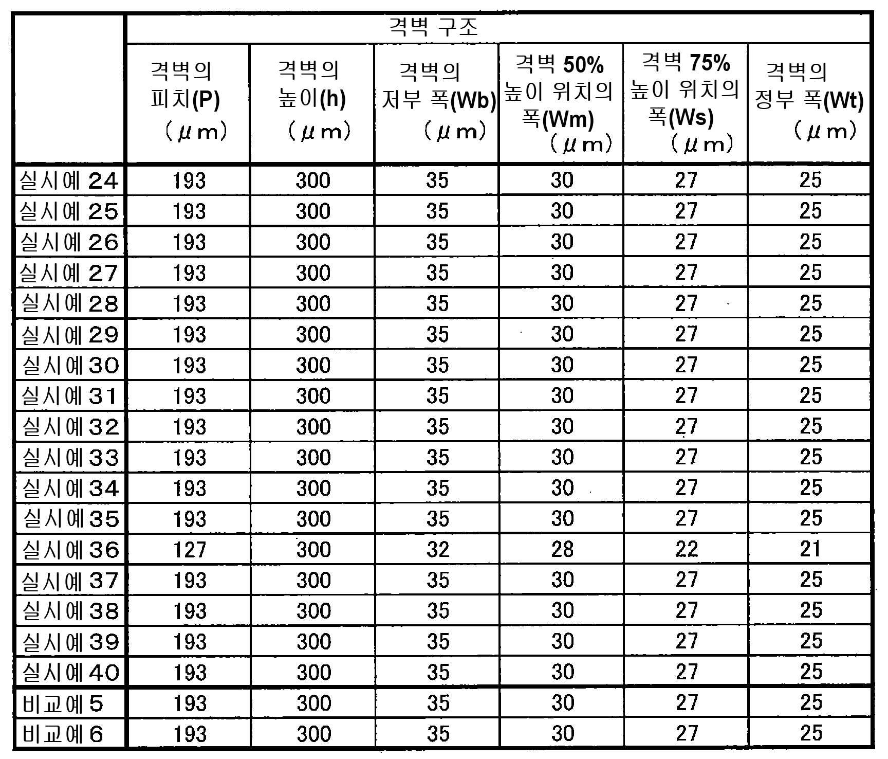
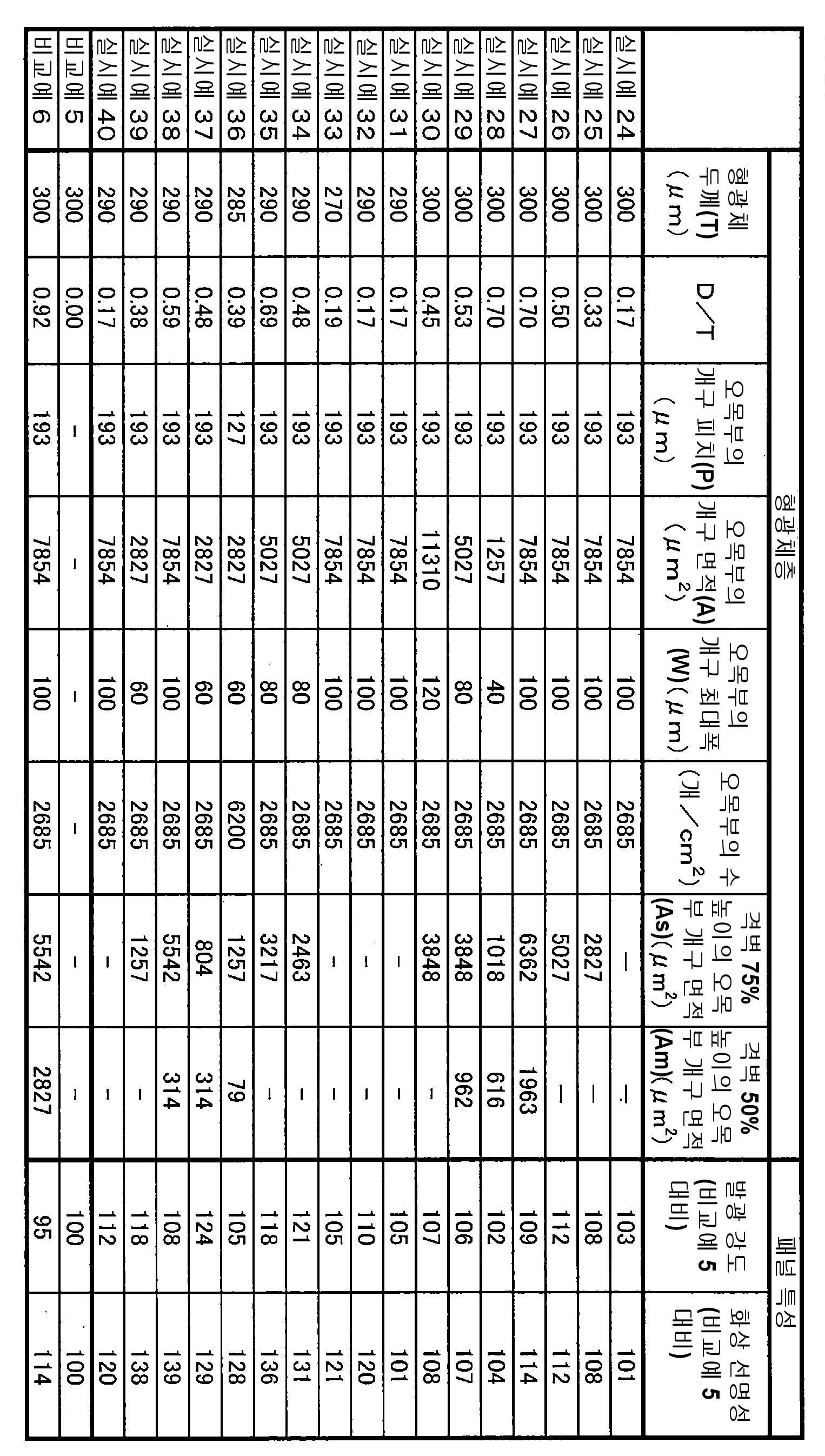
1
방사선 화상 검출 장치
2
신틸레이터 패널
3
검출 기판
4
기판
5
완충층
6
격벽
7
형광체층
8
반사층
9
접착층
10
광전 변환층
11
출력층
12
기판
13
전원부1 Radiographic
3
5
7
9
11
13 Power supply
Claims (8)
상기 형광체층은 표면에 복수의 오목부를 갖고,
상기 오목부의 개구부의 면적(A)은 500~70000㎛2이며,
상기 형광체층의 두께(T)와 상기 오목부의 깊이(D)의 비인 D/T는 0.1~0.9인 신틸레이터 패널.A scintillator panel comprising a substrate and a phosphor layer containing a phosphor powder,
Wherein the phosphor layer has a plurality of concave portions on its surface,
The area A of the opening of the concave portion is 500 to 70000 탆 2 ,
Wherein a ratio D / T of the thickness (T) of the phosphor layer to a depth (D) of the concave portion is 0.1 to 0.9.
상기 형광체층은 표면에 500~50000개/㎠의 오목부를 갖는 신틸레이터 패널.The method according to claim 1,
Wherein the phosphor layer has a concave portion on the surface of 500 to 50,000 / cm < 2 >.
인접하는 상기 오목부끼리의 피치(P)는 50~350㎛의 범위에 있어서의 일정값이며,
상기 오목부의 개구부의 최대폭(W)은 30~300㎛인 신틸레이터 패널.3. The method according to claim 1 or 2,
The pitch P between adjacent concave portions is a constant value in the range of 50 to 350 mu m,
And a maximum width (W) of an opening of the concave portion is 30 to 300 mu m.
상기 형광체층을 구획하는 격벽을 더 갖는 신틸레이터 패널.4. The method according to any one of claims 1 to 3,
And a partition wall separating the phosphor layer.
상기 형광체층과 상기 격벽 사이에 오목 형상의 반사층을 더 구비하는 신틸레이터 패널.5. The method of claim 4,
And a concave reflective layer between the phosphor layer and the barrier rib.
상기 형광체층은 상기 형광체 분말의 충전 밀도가 다른 복수의 층으로 구성되어 있는 신틸레이터 패널.6. The method according to any one of claims 1 to 5,
Wherein the phosphor layer is composed of a plurality of layers having different filling densities of the phosphor powders.
A manufacturing method of a radiation image detecting apparatus comprising a scintillator panel according to any one of claims 1 to 7 and a detection substrate including a photoelectric conversion element facing the concave portion of the scintillator panel, A) a step of positioning the concave portion and the photoelectric conversion element; and (B) a step of bonding the scintillator panel and the detection substrate.
Applications Claiming Priority (3)
| Application Number | Priority Date | Filing Date | Title |
|---|---|---|---|
| JPJP-P-2014-112067 | 2014-05-30 | ||
| JP2014112067 | 2014-05-30 | ||
| PCT/JP2015/064780 WO2015182524A1 (en) | 2014-05-30 | 2015-05-22 | Scintillator panel, radiographic image detection device, and method for manufacturing same |
Publications (2)
| Publication Number | Publication Date |
|---|---|
| KR20170010352A true KR20170010352A (en) | 2017-01-31 |
| KR102122746B1 KR102122746B1 (en) | 2020-06-15 |
Family
ID=54698856
Family Applications (1)
| Application Number | Title | Priority Date | Filing Date |
|---|---|---|---|
| KR1020167028781A Active KR102122746B1 (en) | 2014-05-30 | 2015-05-22 | Scintillator panel, radiographic image detection device, and method for manufacturing same |
Country Status (7)
| Country | Link |
|---|---|
| US (1) | US10042060B2 (en) |
| EP (1) | EP3151247B1 (en) |
| JP (1) | JP6593169B2 (en) |
| KR (1) | KR102122746B1 (en) |
| CN (1) | CN106463194B (en) |
| TW (1) | TWI665463B (en) |
| WO (1) | WO2015182524A1 (en) |
Families Citing this family (11)
| Publication number | Priority date | Publication date | Assignee | Title |
|---|---|---|---|---|
| US9650569B1 (en) * | 2015-11-25 | 2017-05-16 | Siemens Medical Solutions Usa, Inc. | Method of manufacturing garnet interfaces and articles containing the garnets obtained therefrom |
| KR102113461B1 (en) * | 2016-06-01 | 2020-05-22 | 미쯔비시 케미컬 주식회사 | Radiation image conversion screen and flat panel detector |
| CN107658361A (en) | 2016-07-25 | 2018-02-02 | 群创光电股份有限公司 | Active Matrix Image Sensing Device |
| JP2019023579A (en) * | 2017-07-24 | 2019-02-14 | コニカミノルタ株式会社 | Scintillator |
| JP6877289B2 (en) * | 2017-07-31 | 2021-05-26 | キヤノン株式会社 | Manufacturing method of radiation detection device, radiation detection system, and radiation emission device |
| JP6898193B2 (en) * | 2017-09-27 | 2021-07-07 | 浜松ホトニクス株式会社 | Scintillator panel and radiation detector |
| CN115176176B (en) * | 2020-03-05 | 2025-06-20 | 富士胶片株式会社 | Radiation detector, radiation imaging device, and method for manufacturing radiation detector |
| WO2021256011A1 (en) * | 2020-06-16 | 2021-12-23 | 浜松ホトニクス株式会社 | Scintillator panel and radiation detector |
| WO2021255853A1 (en) * | 2020-06-17 | 2021-12-23 | 株式会社日立ハイテク | Device for detecting charged particles or radiation |
| US12392912B2 (en) * | 2020-12-25 | 2025-08-19 | Toray Industries, Inc. | Scintillator panel, radiation detector, radiation inspection device, and method for producing scintillator panel |
| CN115926785B (en) * | 2022-08-12 | 2024-08-16 | 成都信息工程大学 | Scintillator layer material, flexible scintillator panel and preparation method and application thereof |
Citations (9)
| Publication number | Priority date | Publication date | Assignee | Title |
|---|---|---|---|---|
| JPH0560871A (en) | 1991-09-04 | 1993-03-12 | Hamamatsu Photonics Kk | Radiation detection element |
| US20020191743A1 (en) * | 2001-05-23 | 2002-12-19 | Hartmut Sklebitz | Solid-state radiation detector |
| JP2003082347A (en) * | 2001-06-25 | 2003-03-19 | Kasei Optonix Co Ltd | Gadolinium oxysulfide phosphor for digital radiography, radiation image conversion screen, and radiation image imaging device |
| JP2003215253A (en) | 2002-01-23 | 2003-07-30 | Canon Inc | Radiation-detecting device and manufacturing method thereof, and radiation detection system |
| WO2010010725A1 (en) * | 2008-07-25 | 2010-01-28 | コニカミノルタエムジー株式会社 | Scintillator panel and radiographic image detector provided with the same |
| JP2011007552A (en) | 2009-06-24 | 2011-01-13 | Konica Minolta Medical & Graphic Inc | Scintillator panel, radiation detection device, and method of manufacturing the scintillator panel |
| JP2011188148A (en) | 2010-03-05 | 2011-09-22 | Toshiba Corp | Solid imaging device |
| JP2012058170A (en) * | 2010-09-13 | 2012-03-22 | Konica Minolta Medical & Graphic Inc | Scintillator panel |
| JP2012242355A (en) | 2011-05-24 | 2012-12-10 | Fujifilm Corp | Radiation detection device |
Family Cites Families (15)
| Publication number | Priority date | Publication date | Assignee | Title |
|---|---|---|---|---|
| US4208470A (en) * | 1978-11-03 | 1980-06-17 | General Electric Company | X-ray intensifying screen |
| DE3578359D1 (en) * | 1984-12-17 | 1990-07-26 | Konishiroku Photo Ind | SCREEN FOR SAVING A RADIATION IMAGE. |
| US5219606A (en) * | 1989-05-23 | 1993-06-15 | Kabushiki Kaisha Toshiba | Method of manufacturing phosphor screen for intensifier |
| JPH09325185A (en) * | 1996-06-03 | 1997-12-16 | Toshiba Fa Syst Eng Kk | Radiation detector, its manufacture, fluorographic apparatus and ct scanner |
| US6177236B1 (en) * | 1997-12-05 | 2001-01-23 | Xerox Corporation | Method of making a pixelized scintillation layer and structures incorporating same |
| EP1127098A4 (en) | 1998-08-27 | 2006-05-24 | Superior Micropowders Llc | PHOSPHORUS POWDERS, METHODS OF MAKING PHOSPHORUS POWDERS, AND DEVICES INCLUDING THE SAME |
| JP2002122672A (en) * | 2000-10-12 | 2002-04-26 | Canon Inc | Imaging device and radiation imaging system including the same |
| JP4647828B2 (en) * | 2001-05-07 | 2011-03-09 | 浜松ホトニクス株式会社 | Scintillator panel and radiation detector using the same |
| DE102005010077B4 (en) * | 2005-03-04 | 2007-09-20 | Siemens Ag | Detector with a scintillator and imaging device, comprising such a detector |
| JP2008014853A (en) | 2006-07-07 | 2008-01-24 | Fujifilm Corp | Radiation image conversion panel and method for manufacturing radiation image conversion panel |
| CN101777480A (en) * | 2009-01-13 | 2010-07-14 | 李腾 | X-ray fluorescent screen with function of improving luminance and method thereof |
| JP5686724B2 (en) * | 2009-02-23 | 2015-03-18 | 株式会社東芝 | Solid scintillator, radiation detector, and X-ray tomography apparatus |
| JP5340444B2 (en) | 2012-03-12 | 2013-11-13 | 富士フイルム株式会社 | Radiographic image detection apparatus and radiographic imaging system |
| JPWO2014021415A1 (en) * | 2012-08-03 | 2016-07-21 | 東レ株式会社 | Scintillator panel and method for manufacturing scintillator panel |
| JP5488773B1 (en) * | 2012-10-03 | 2014-05-14 | 東レ株式会社 | Scintillator panel and method for manufacturing scintillator panel |
-
2015
- 2015-05-22 EP EP15799767.7A patent/EP3151247B1/en active Active
- 2015-05-22 US US15/314,707 patent/US10042060B2/en active Active
- 2015-05-22 JP JP2015528744A patent/JP6593169B2/en active Active
- 2015-05-22 WO PCT/JP2015/064780 patent/WO2015182524A1/en not_active Ceased
- 2015-05-22 KR KR1020167028781A patent/KR102122746B1/en active Active
- 2015-05-22 CN CN201580028088.0A patent/CN106463194B/en active Active
- 2015-05-27 TW TW104116916A patent/TWI665463B/en active
Patent Citations (10)
| Publication number | Priority date | Publication date | Assignee | Title |
|---|---|---|---|---|
| JPH0560871A (en) | 1991-09-04 | 1993-03-12 | Hamamatsu Photonics Kk | Radiation detection element |
| US20020191743A1 (en) * | 2001-05-23 | 2002-12-19 | Hartmut Sklebitz | Solid-state radiation detector |
| JP2003082347A (en) * | 2001-06-25 | 2003-03-19 | Kasei Optonix Co Ltd | Gadolinium oxysulfide phosphor for digital radiography, radiation image conversion screen, and radiation image imaging device |
| JP2003215253A (en) | 2002-01-23 | 2003-07-30 | Canon Inc | Radiation-detecting device and manufacturing method thereof, and radiation detection system |
| WO2010010725A1 (en) * | 2008-07-25 | 2010-01-28 | コニカミノルタエムジー株式会社 | Scintillator panel and radiographic image detector provided with the same |
| JP2013117547A (en) | 2008-07-25 | 2013-06-13 | Konica Minolta Medical & Graphic Inc | Radiation image detection device |
| JP2011007552A (en) | 2009-06-24 | 2011-01-13 | Konica Minolta Medical & Graphic Inc | Scintillator panel, radiation detection device, and method of manufacturing the scintillator panel |
| JP2011188148A (en) | 2010-03-05 | 2011-09-22 | Toshiba Corp | Solid imaging device |
| JP2012058170A (en) * | 2010-09-13 | 2012-03-22 | Konica Minolta Medical & Graphic Inc | Scintillator panel |
| JP2012242355A (en) | 2011-05-24 | 2012-12-10 | Fujifilm Corp | Radiation detection device |
Also Published As
| Publication number | Publication date |
|---|---|
| JP6593169B2 (en) | 2019-10-23 |
| TW201602618A (en) | 2016-01-16 |
| EP3151247A1 (en) | 2017-04-05 |
| TWI665463B (en) | 2019-07-11 |
| US20170192105A1 (en) | 2017-07-06 |
| EP3151247A4 (en) | 2018-02-14 |
| CN106463194A (en) | 2017-02-22 |
| WO2015182524A1 (en) | 2015-12-03 |
| KR102122746B1 (en) | 2020-06-15 |
| US10042060B2 (en) | 2018-08-07 |
| CN106463194B (en) | 2018-09-07 |
| JPWO2015182524A1 (en) | 2017-04-20 |
| EP3151247B1 (en) | 2020-11-25 |
Similar Documents
| Publication | Publication Date | Title |
|---|---|---|
| KR102122746B1 (en) | Scintillator panel, radiographic image detection device, and method for manufacturing same | |
| KR102098124B1 (en) | Scintillator panel | |
| JP5110230B1 (en) | Scintillator panel and method for manufacturing scintillator panel | |
| JP6256006B2 (en) | Scintillator panel and manufacturing method thereof | |
| KR102099091B1 (en) | Method for manufacturing three-dimensional structure, method for manufacturing scintillator panel, three-dimensional structure, and scintillator panel | |
| JP5704260B2 (en) | Scintillator panel | |
| JPWO2014069284A1 (en) | Radiation detection apparatus and manufacturing method thereof | |
| TWI612535B (en) | Scintillator panel and method for manufacturing scintillator panel | |
| WO2014021415A1 (en) | Scintillator panel and method for producing scintillator panel | |
| JP6217076B2 (en) | Scintillator panel and method for manufacturing scintillator panel | |
| JP6003623B2 (en) | Scintillator panel and method for manufacturing scintillator panel |
Legal Events
| Date | Code | Title | Description |
|---|---|---|---|
| PA0105 | International application |
Patent event date: 20161017 Patent event code: PA01051R01D Comment text: International Patent Application |
|
| PG1501 | Laying open of application | ||
| A201 | Request for examination | ||
| A302 | Request for accelerated examination | ||
| PA0201 | Request for examination |
Patent event code: PA02012R01D Patent event date: 20200116 Comment text: Request for Examination of Application |
|
| PA0302 | Request for accelerated examination |
Patent event date: 20200116 Patent event code: PA03022R01D Comment text: Request for Accelerated Examination |
|
| E902 | Notification of reason for refusal | ||
| PE0902 | Notice of grounds for rejection |
Comment text: Notification of reason for refusal Patent event date: 20200320 Patent event code: PE09021S01D |
|
| E701 | Decision to grant or registration of patent right | ||
| PE0701 | Decision of registration |
Patent event code: PE07011S01D Comment text: Decision to Grant Registration Patent event date: 20200602 |
|
| GRNT | Written decision to grant | ||
| PR0701 | Registration of establishment |
Comment text: Registration of Establishment Patent event date: 20200609 Patent event code: PR07011E01D |
|
| PR1002 | Payment of registration fee |
Payment date: 20200610 End annual number: 3 Start annual number: 1 |
|
| PG1601 | Publication of registration | ||
| PR1001 | Payment of annual fee |
Payment date: 20240520 Start annual number: 5 End annual number: 5 |