KR20170010697A - 점착 기능을 구비한 유연 전자소자 및 그의 제조방법 - Google Patents
점착 기능을 구비한 유연 전자소자 및 그의 제조방법 Download PDFInfo
- Publication number
- KR20170010697A KR20170010697A KR1020150102689A KR20150102689A KR20170010697A KR 20170010697 A KR20170010697 A KR 20170010697A KR 1020150102689 A KR1020150102689 A KR 1020150102689A KR 20150102689 A KR20150102689 A KR 20150102689A KR 20170010697 A KR20170010697 A KR 20170010697A
- Authority
- KR
- South Korea
- Prior art keywords
- layer
- electronic device
- adhesive tape
- adhesive
- gate insulating
- Prior art date
- Legal status (The legal status is an assumption and is not a legal conclusion. Google has not performed a legal analysis and makes no representation as to the accuracy of the status listed.)
- Ceased
Links
Images



Classifications
-
- H—ELECTRICITY
- H10—SEMICONDUCTOR DEVICES; ELECTRIC SOLID-STATE DEVICES NOT OTHERWISE PROVIDED FOR
- H10D—INORGANIC ELECTRIC SEMICONDUCTOR DEVICES
- H10D30/00—Field-effect transistors [FET]
- H10D30/60—Insulated-gate field-effect transistors [IGFET]
- H10D30/67—Thin-film transistors [TFT]
- H10D30/674—Thin-film transistors [TFT] characterised by the active materials
- H10D30/6741—Group IV materials, e.g. germanium or silicon carbide
-
- H01L51/0097—
-
- H01L21/67132—
-
- H—ELECTRICITY
- H10—SEMICONDUCTOR DEVICES; ELECTRIC SOLID-STATE DEVICES NOT OTHERWISE PROVIDED FOR
- H10D—INORGANIC ELECTRIC SEMICONDUCTOR DEVICES
- H10D30/00—Field-effect transistors [FET]
- H10D30/01—Manufacture or treatment
-
- H—ELECTRICITY
- H10—SEMICONDUCTOR DEVICES; ELECTRIC SOLID-STATE DEVICES NOT OTHERWISE PROVIDED FOR
- H10D—INORGANIC ELECTRIC SEMICONDUCTOR DEVICES
- H10D30/00—Field-effect transistors [FET]
- H10D30/01—Manufacture or treatment
- H10D30/017—Manufacture or treatment of FETs having two-dimensional material channels, e.g. TMD FETs
-
- H—ELECTRICITY
- H10—SEMICONDUCTOR DEVICES; ELECTRIC SOLID-STATE DEVICES NOT OTHERWISE PROVIDED FOR
- H10D—INORGANIC ELECTRIC SEMICONDUCTOR DEVICES
- H10D30/00—Field-effect transistors [FET]
- H10D30/40—FETs having zero-dimensional [0D], one-dimensional [1D] or two-dimensional [2D] charge carrier gas channels
- H10D30/47—FETs having zero-dimensional [0D], one-dimensional [1D] or two-dimensional [2D] charge carrier gas channels having two-dimensional [2D] charge carrier gas channels, e.g. nanoribbon FETs or high electron mobility transistors [HEMT]
- H10D30/481—FETs having two-dimensional material channels, e.g. transition metal dichalcogenide [TMD] FETs
-
- H—ELECTRICITY
- H10—SEMICONDUCTOR DEVICES; ELECTRIC SOLID-STATE DEVICES NOT OTHERWISE PROVIDED FOR
- H10D—INORGANIC ELECTRIC SEMICONDUCTOR DEVICES
- H10D30/00—Field-effect transistors [FET]
- H10D30/60—Insulated-gate field-effect transistors [IGFET]
- H10D30/67—Thin-film transistors [TFT]
- H10D30/6758—Thin-film transistors [TFT] characterised by the insulating substrates
-
- H—ELECTRICITY
- H10—SEMICONDUCTOR DEVICES; ELECTRIC SOLID-STATE DEVICES NOT OTHERWISE PROVIDED FOR
- H10D—INORGANIC ELECTRIC SEMICONDUCTOR DEVICES
- H10D62/00—Semiconductor bodies, or regions thereof, of devices having potential barriers
- H10D62/80—Semiconductor bodies, or regions thereof, of devices having potential barriers characterised by the materials
- H10D62/83—Semiconductor bodies, or regions thereof, of devices having potential barriers characterised by the materials being Group IV materials, e.g. B-doped Si or undoped Ge
- H10D62/8303—Diamond
-
- H—ELECTRICITY
- H10—SEMICONDUCTOR DEVICES; ELECTRIC SOLID-STATE DEVICES NOT OTHERWISE PROVIDED FOR
- H10D—INORGANIC ELECTRIC SEMICONDUCTOR DEVICES
- H10D62/00—Semiconductor bodies, or regions thereof, of devices having potential barriers
- H10D62/80—Semiconductor bodies, or regions thereof, of devices having potential barriers characterised by the materials
- H10D62/881—Semiconductor bodies, or regions thereof, of devices having potential barriers characterised by the materials being a two-dimensional material
- H10D62/882—Graphene
-
- H—ELECTRICITY
- H10—SEMICONDUCTOR DEVICES; ELECTRIC SOLID-STATE DEVICES NOT OTHERWISE PROVIDED FOR
- H10D—INORGANIC ELECTRIC SEMICONDUCTOR DEVICES
- H10D64/00—Electrodes of devices having potential barriers
- H10D64/20—Electrodes characterised by their shapes, relative sizes or dispositions
- H10D64/27—Electrodes not carrying the current to be rectified, amplified, oscillated or switched, e.g. gates
- H10D64/311—Gate electrodes for field-effect devices
- H10D64/411—Gate electrodes for field-effect devices for FETs
- H10D64/511—Gate electrodes for field-effect devices for FETs for IGFETs
- H10D64/512—Disposition of the gate electrodes, e.g. buried gates
-
- H—ELECTRICITY
- H10—SEMICONDUCTOR DEVICES; ELECTRIC SOLID-STATE DEVICES NOT OTHERWISE PROVIDED FOR
- H10D—INORGANIC ELECTRIC SEMICONDUCTOR DEVICES
- H10D64/00—Electrodes of devices having potential barriers
- H10D64/20—Electrodes characterised by their shapes, relative sizes or dispositions
- H10D64/27—Electrodes not carrying the current to be rectified, amplified, oscillated or switched, e.g. gates
- H10D64/311—Gate electrodes for field-effect devices
- H10D64/411—Gate electrodes for field-effect devices for FETs
- H10D64/511—Gate electrodes for field-effect devices for FETs for IGFETs
- H10D64/514—Gate electrodes for field-effect devices for FETs for IGFETs characterised by the insulating layers
-
- H—ELECTRICITY
- H10—SEMICONDUCTOR DEVICES; ELECTRIC SOLID-STATE DEVICES NOT OTHERWISE PROVIDED FOR
- H10K—ORGANIC ELECTRIC SOLID-STATE DEVICES
- H10K10/00—Organic devices specially adapted for rectifying, amplifying, oscillating or switching; Organic capacitors or resistors having potential barriers
- H10K10/40—Organic transistors
- H10K10/46—Field-effect transistors, e.g. organic thin-film transistors [OTFT]
- H10K10/462—Insulated gate field-effect transistors [IGFETs]
- H10K10/466—Lateral bottom-gate IGFETs comprising only a single gate
-
- H—ELECTRICITY
- H10—SEMICONDUCTOR DEVICES; ELECTRIC SOLID-STATE DEVICES NOT OTHERWISE PROVIDED FOR
- H10K—ORGANIC ELECTRIC SOLID-STATE DEVICES
- H10K10/00—Organic devices specially adapted for rectifying, amplifying, oscillating or switching; Organic capacitors or resistors having potential barriers
- H10K10/40—Organic transistors
- H10K10/46—Field-effect transistors, e.g. organic thin-film transistors [OTFT]
- H10K10/462—Insulated gate field-effect transistors [IGFETs]
- H10K10/468—Insulated gate field-effect transistors [IGFETs] characterised by the gate dielectrics
-
- H—ELECTRICITY
- H10—SEMICONDUCTOR DEVICES; ELECTRIC SOLID-STATE DEVICES NOT OTHERWISE PROVIDED FOR
- H10K—ORGANIC ELECTRIC SOLID-STATE DEVICES
- H10K10/00—Organic devices specially adapted for rectifying, amplifying, oscillating or switching; Organic capacitors or resistors having potential barriers
- H10K10/40—Organic transistors
- H10K10/46—Field-effect transistors, e.g. organic thin-film transistors [OTFT]
- H10K10/462—Insulated gate field-effect transistors [IGFETs]
- H10K10/484—Insulated gate field-effect transistors [IGFETs] characterised by the channel regions
-
- H—ELECTRICITY
- H10—SEMICONDUCTOR DEVICES; ELECTRIC SOLID-STATE DEVICES NOT OTHERWISE PROVIDED FOR
- H10K—ORGANIC ELECTRIC SOLID-STATE DEVICES
- H10K77/00—Constructional details of devices covered by this subclass and not covered by groups H10K10/80, H10K30/80, H10K50/80 or H10K59/80
- H10K77/10—Substrates, e.g. flexible substrates
- H10K77/111—Flexible substrates
-
- H—ELECTRICITY
- H10—SEMICONDUCTOR DEVICES; ELECTRIC SOLID-STATE DEVICES NOT OTHERWISE PROVIDED FOR
- H10K—ORGANIC ELECTRIC SOLID-STATE DEVICES
- H10K85/00—Organic materials used in the body or electrodes of devices covered by this subclass
- H10K85/10—Organic polymers or oligomers
- H10K85/141—Organic polymers or oligomers comprising aliphatic or olefinic chains, e.g. poly N-vinylcarbazol, PVC or PTFE
- H10K85/143—Polyacetylene; Derivatives thereof
-
- H—ELECTRICITY
- H10—SEMICONDUCTOR DEVICES; ELECTRIC SOLID-STATE DEVICES NOT OTHERWISE PROVIDED FOR
- H10P—GENERIC PROCESSES OR APPARATUS FOR THE MANUFACTURE OR TREATMENT OF DEVICES COVERED BY CLASS H10
- H10P14/00—Formation of materials, e.g. in the shape of layers or pillars
- H10P14/20—Formation of materials, e.g. in the shape of layers or pillars of semiconductor materials
- H10P14/34—Deposited materials, e.g. layers
- H10P14/3402—Deposited materials, e.g. layers characterised by the chemical composition
- H10P14/3404—Deposited materials, e.g. layers characterised by the chemical composition being Group IVA materials
- H10P14/3406—Carbon, e.g. diamond-like carbon
-
- H—ELECTRICITY
- H10—SEMICONDUCTOR DEVICES; ELECTRIC SOLID-STATE DEVICES NOT OTHERWISE PROVIDED FOR
- H10P—GENERIC PROCESSES OR APPARATUS FOR THE MANUFACTURE OR TREATMENT OF DEVICES COVERED BY CLASS H10
- H10P14/00—Formation of materials, e.g. in the shape of layers or pillars
- H10P14/60—Formation of materials, e.g. in the shape of layers or pillars of insulating materials
- H10P14/63—Formation of materials, e.g. in the shape of layers or pillars of insulating materials characterised by the formation processes
- H10P14/6302—Non-deposition formation processes
- H10P14/6304—Formation by oxidation, e.g. oxidation of the substrate
-
- H—ELECTRICITY
- H10—SEMICONDUCTOR DEVICES; ELECTRIC SOLID-STATE DEVICES NOT OTHERWISE PROVIDED FOR
- H10P—GENERIC PROCESSES OR APPARATUS FOR THE MANUFACTURE OR TREATMENT OF DEVICES COVERED BY CLASS H10
- H10P14/00—Formation of materials, e.g. in the shape of layers or pillars
- H10P14/60—Formation of materials, e.g. in the shape of layers or pillars of insulating materials
- H10P14/63—Formation of materials, e.g. in the shape of layers or pillars of insulating materials characterised by the formation processes
- H10P14/6302—Non-deposition formation processes
- H10P14/6319—Formation by plasma treatments, e.g. plasma oxidation of the substrate
-
- Y—GENERAL TAGGING OF NEW TECHNOLOGICAL DEVELOPMENTS; GENERAL TAGGING OF CROSS-SECTIONAL TECHNOLOGIES SPANNING OVER SEVERAL SECTIONS OF THE IPC; TECHNICAL SUBJECTS COVERED BY FORMER USPC CROSS-REFERENCE ART COLLECTIONS [XRACs] AND DIGESTS
- Y02—TECHNOLOGIES OR APPLICATIONS FOR MITIGATION OR ADAPTATION AGAINST CLIMATE CHANGE
- Y02E—REDUCTION OF GREENHOUSE GAS [GHG] EMISSIONS, RELATED TO ENERGY GENERATION, TRANSMISSION OR DISTRIBUTION
- Y02E10/00—Energy generation through renewable energy sources
- Y02E10/50—Photovoltaic [PV] energy
- Y02E10/549—Organic PV cells
-
- Y—GENERAL TAGGING OF NEW TECHNOLOGICAL DEVELOPMENTS; GENERAL TAGGING OF CROSS-SECTIONAL TECHNOLOGIES SPANNING OVER SEVERAL SECTIONS OF THE IPC; TECHNICAL SUBJECTS COVERED BY FORMER USPC CROSS-REFERENCE ART COLLECTIONS [XRACs] AND DIGESTS
- Y02—TECHNOLOGIES OR APPLICATIONS FOR MITIGATION OR ADAPTATION AGAINST CLIMATE CHANGE
- Y02P—CLIMATE CHANGE MITIGATION TECHNOLOGIES IN THE PRODUCTION OR PROCESSING OF GOODS
- Y02P70/00—Climate change mitigation technologies in the production process for final industrial or consumer products
- Y02P70/50—Manufacturing or production processes characterised by the final manufactured product
Landscapes
- Chemical & Material Sciences (AREA)
- Engineering & Computer Science (AREA)
- Materials Engineering (AREA)
- Thin Film Transistor (AREA)
Abstract
Description
도 2는 실시예 1에 따라 실리콘 웨이퍼 상에 제조된 점착 기능을 구비한 유연 전자소자의 개략도 및 측단면도(a) 및 실리콘 웨이퍼에서 분리한 점착 기능을 구비한 유연 전자소자의 사진(b)을 나타낸 것이다.
도3은 스카치 테이프 표면에 폴리이미드의 코팅 전 후 거칠기를 비교한 AFM(atomic force microscope) 이미지이다.
도 4는 실시예 1에 의해 제조된 그래핀 전계효과 트랜지스터를 지폐, 실리콘 웨이퍼, 종이에 부착한 이미지 및 각각의 전기적 성능을 분석하여 나타낸 그래프이다.
도 5는 실시예 1 내지 3에 의해 제조된 게이트절연층의 누설전류밀도(current density)를 측정하여 나타낸 그래프이다.
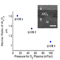
도 6은 실시예 1 내지 3에 의해 제조된 그래핀 전계효과 트랜지스터의 산소 플라즈마 압력에 따른 AlOX의 원자비를 측정하여 나타낸 그래프 및 및 TEM(transmission electron microscope) 이미지이다.
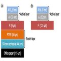
도 7은 실시예 1에 따라 제조된 게이트절연층/게이트 패턴/폴리이미드/접착테이프가 오피스 페이퍼(office paper)에 부착된 게이트절연층/게이트 패턴/폴리이미드/접착테이프/오피스 페이퍼(a)의 측단면 및 비교예 1에 따라 제조된 게이트 절연층/게이트 패턴/폴리이미드(b)의 측단면을 나타낸 것이다.
도 8은 도 7의 두 샘플에 대한 구부림 곡률반경(bending radius)에 따른 표면 변형률(surface strain)을 측정하여 나타낸 것이다.
Claims (20)
- 유연 필름, 및 상기 유연 필름의 일측면 상에 형성된 점착층을 포함하는 점착테이프; 및
상기 점착테이프의 상기 일측면의 반대측 타측면 상에 형성된 전자소자;를
포함하는 점착 기능을 구비한 유연 전자소자. - 제1항에 있어서,
상기 전자소자가 상기 유연 필름을 기판으로 포함하는 것을 특징으로 하는 점착 기능을 구비한 유연 전자소자. - 제1항에 있어서,
상기 유연 전자소자가 전계효과 트랜지스터, 태양전지, 유기발광다이오드, 촉각센서, 전파 식별 태그, 전자종이, 및 바이오 센서 중에서 선택된 1종 이상인 것을 특징으로 하는 점착 기능을 구비한 유연 전자소자. - 제3항에 있어서,
상기 점착 기능을 구비한 유연 전자소자가 전계효과 트랜지스터이고,
상기 전계효과 트랜지스터가
유연 필름, 및 상기 유연 필름의 일측면 상에 형성된 점착층을 포함하는 점착테이프;
상기 점착테이프의 상기 일측면의 반대측 타측면 상에 위치하는 게이트 전극;
상기 게이트 전극 상에 위치하는 게이트 절연층;
상기 게이트 절연층 상에 위치하고, 서로 이격되어 배치되는 소스 전극 및 드레인 전극; 및
상기 게이트 절연층 상에 위치하고 상기 소스전극 및 드레인 전극을 전기적으로 연결하는 활성층;을 포함하는 것을 특징으로 하는 점착 기능을 구비한 유연 전자소자. - 제4항에 있어서,
상기 점착테이프는 상기 타측면 상에 상기 타측면의 표면을 평탄화하는 표면개질층을 추가로 포함하는 것을 특징으로 하는 점착 기능을 구비한 유연 전자소자. - 제5항에 있어서,
상기 표면개질층이 폴리이미드(polyimide), 폴리아크릴레이트, 폴리우레탄, 폴리에틸렌, 폴리비닐페놀, 및 폴리비닐알콜 중에서 선택된 1종 이상을 포함하는 것을 특징으로 하는 점착 기능을 구비한 유연 전자소자. - 제4항에 있어서,
상기 점착테이프의 영탄성률(Young's modulus)이 상기 표면 개질층의 영탄성률(Young's modulus) 보다 작은 것을 특징으로 하는 점착 기능을 구비한 유연 전자소자. - 제5항에 있어서,
상기 표면 개질층은 제곱평균제곱근 거칠기(Root-mean-square roughness)가 0.1 내지 1 nm인 것을 특징으로 하는 점착 기능을 구비한 유연 전자소자. - 제4항에 있어서,
상기 게이트 절연층은 두께가 1 내지 10 nm인 것을 특징으로 하는 점착 기능을 구비한 전자소자. - 제4항에 있어서,
상기 활성층이 그래핀, PQT-12(poly(3,3'''-didodecyl quarterthiophene)), P3HT(poly(3-hexyl thiophene)), P3BT(poly(3-butyl thiophene)), P3OT(poly(3-octyl thiophene)), PPy(polypyrrole), PANI(polyaniline), PDPP(polydiketopyrrolopyrrole), PIID(polyisoindigo), PPDI(poly(perylene diimide)), PNDI(poly(naphthalene diimide)), PEO(poly(ethylene oxide)), PCL(poly(-caprolactone)), PMMA(poly(methyl methacrylate)), PS(polystyrene), PVP (poly(vinyl pyrrolidone)), 펜타센, 루브린, 구리 프탈로시아닌 및 풀러렌 중에서 선택된 1종 이상을 포함하는 것을 특징으로 하는 점착 기능을 구비한 유연 전자소자. - (a) 유연 필름, 및 상기 유연 필름의 일측면 상에 형성된 점착층을 포함하는 점착테이프를 준비하는 단계; 및
(b) 상기 점착테이프의 상기 일측면의 반대측 타측면 상에 전자소자를 형성하는 단계;를
포함하는 점착 기능을 구비한 유연 전자소자의 제조방법. - 제11항에 있어서,
상기 유연 전자소자의 제조방법이 단계 (a) 후에 상기 점착테이프의 상기 일측면의 반대측 타측면 상에 표면개질층을 코팅하는 단계를 추가로 포함하는 것을 특징으로 하는 점착 기능을 구비한 유연 전자소자의 제조방법. - 제11항에 있어서,
단계 (b)의 전자소자가 전계효과 트랜지스터, 태양전지, 유기발광다이오드, 촉각센서, 전파 식별 태그, 전자종이, 및 바이오 센서 중에서 선택된 1종 이상인 것을 특징으로 하는 점착 기능을 구비한 유연 전자소자의 제조방법. - 제13항에 있어서,
단계 (b)의 전자소자가 전계효과 트랜지스터이고,
단계 (b)가,
(b-1) 상기 점착테이프의 상기 일측면의 반대측 타측면 상에 게이트 전극을 형성하는 단계;
(b-2) 상기 게이트 전극상에 게이트 절연층을 형성하는 단계;
(b-3) 상기 게이트 절연층 상에 소스 전극 및 드레인 전극을 형성하는 단계; 및
(b-4) 상기 게이트 절연층 상에, 상기 소스 전극 및 드레인 전극을 전기적으로 연결하는 활성층을 형성하는 단계;를
포함하는 점착 기능을 구비한 유연 전자소자의 제조방법. - 제14항에 있어서,
단계 (b-2)가 UV 오존처리, 산소 분위기 열처리, 및 산소 플라즈마 처리 중에서 선택된 어느 하나의 방법으로 수행되는 것을 특징으로 하는 점착 기능을 구비한 유연 전자소자의 제조방법. - 제15항에 있어서,
단계 (b-2)가 산소 플라즈마 처리에 의해 수행되는 것을 특징으로 하는 점착 기능을 구비한 유연 전자소자의 제조방법. - 제16항에 있어서,
상기 산소 플라즈마 처리가 10 내지 300W의 RF 전력 조건에서 수행되는 것을 특징으로 하는 점착 기능을 구비한 유연 전자소자의 제조방법. - 제16항에 있어서,
상기 산소 플라즈마 처리가 1 내지 1000 mTorr의 압력 조건에서 수행되는 것을 특징으로 하는 점착 기능을 구비한 유연 전자소자의 제조방법. - 제14항에 있어서,
상기 활성층이 그래핀층이고,
상기 그래핀층이 물리적 또는 화학적 박리에 의해 제조된 그래핀, SiC에서 성장시켜 제조된 그래핀, 및 화학기상 증착법에 의해 제조된 그래핀 중에서 선택된 어느 하나인 것을 특징으로 하는 점착 기능을 구비한 유연 전자소자의 제조방법. - 제14항에 있어서,
단계 (b-4)가 건식 전사법에 따라 수행되는 것을 특징으로 하는 점착 기능을 구비한 유연 전자소자의 제조방법.
Priority Applications (2)
| Application Number | Priority Date | Filing Date | Title |
|---|---|---|---|
| KR1020150102689A KR20170010697A (ko) | 2015-07-20 | 2015-07-20 | 점착 기능을 구비한 유연 전자소자 및 그의 제조방법 |
| US14/757,537 US9685558B2 (en) | 2015-07-20 | 2015-12-23 | Flexible electronic device having adhesive function and method of manufacturing the same |
Applications Claiming Priority (1)
| Application Number | Priority Date | Filing Date | Title |
|---|---|---|---|
| KR1020150102689A KR20170010697A (ko) | 2015-07-20 | 2015-07-20 | 점착 기능을 구비한 유연 전자소자 및 그의 제조방법 |
Related Child Applications (1)
| Application Number | Title | Priority Date | Filing Date |
|---|---|---|---|
| KR1020170065981A Division KR20170061125A (ko) | 2017-05-29 | 2017-05-29 | 점착 기능을 구비한 유연 전자소자 및 그의 제조방법 |
Publications (1)
| Publication Number | Publication Date |
|---|---|
| KR20170010697A true KR20170010697A (ko) | 2017-02-01 |
Family
ID=57837866
Family Applications (1)
| Application Number | Title | Priority Date | Filing Date |
|---|---|---|---|
| KR1020150102689A Ceased KR20170010697A (ko) | 2015-07-20 | 2015-07-20 | 점착 기능을 구비한 유연 전자소자 및 그의 제조방법 |
Country Status (2)
| Country | Link |
|---|---|
| US (1) | US9685558B2 (ko) |
| KR (1) | KR20170010697A (ko) |
Cited By (1)
| Publication number | Priority date | Publication date | Assignee | Title |
|---|---|---|---|---|
| KR20180127057A (ko) * | 2017-05-19 | 2018-11-28 | 한국기계연구원 | 정전용량 변위 측정용 그래핀 패치 및 이의 제조 방법 및 이를 이용한 변위 측정 시스템 |
Families Citing this family (20)
| Publication number | Priority date | Publication date | Assignee | Title |
|---|---|---|---|---|
| US10830640B2 (en) * | 2016-09-13 | 2020-11-10 | Sony Corporation | Electromagnetic wave detection element, electromagnetic wave sensor, electronic apparatus, and structural body |
| US10885420B2 (en) | 2016-12-14 | 2021-01-05 | Ajay Khoche | Package sealing tape types with varied transducer sampling densities |
| US10482369B2 (en) | 2016-12-14 | 2019-11-19 | Trackonomy Systems, Inc. | Window based locationing of mobile targets using complementary position estimates |
| US11138490B2 (en) | 2016-12-14 | 2021-10-05 | Ajay Khoche | Hierarchical combination of distributed statistics in a monitoring network |
| US11003978B2 (en) | 2016-12-14 | 2021-05-11 | Ajay Khoche | Programmable network node roles in hierarchical communications network |
| US10902310B2 (en) | 2016-12-14 | 2021-01-26 | Trackonomy Systems, Inc. | Wireless communications and transducer based event detection platform |
| CN107412882B (zh) * | 2017-08-01 | 2020-04-07 | 浙江理工大学 | 一种贴附柔性人工皮肤感受器的制备方法 |
| WO2020247354A1 (en) | 2019-06-05 | 2020-12-10 | Trackonomy Systems, Inc. | Temperature monitoring in cold supply chains |
| CN110148643B (zh) * | 2019-06-06 | 2021-05-04 | 上海纳米技术及应用国家工程研究中心有限公司 | 半导体量子点/石墨烯范德瓦尔斯结柔性器件的构筑方法 |
| US11317516B2 (en) | 2019-09-13 | 2022-04-26 | Trackonomy Systems, Inc. | Roll-to-roll additive manufacturing method and device |
| CN110707216B (zh) * | 2019-10-24 | 2023-06-13 | 宁波石墨烯创新中心有限公司 | 石墨烯薄膜晶体管、其制备方法及显示装置 |
| US11864058B1 (en) | 2020-10-04 | 2024-01-02 | Trackonomy Systems, Inc. | Flexible tracking device for cables and equipment |
| EP4186053A4 (en) | 2020-07-24 | 2024-09-04 | Trackonomy Systems, Inc. | TEAR TO ACTIVATE A WIRELESS NODE WITH MULTIPLE CUTOUTS ALLOWING REUSE |
| US12124904B2 (en) | 2020-09-05 | 2024-10-22 | Trackonomy Systems, Inc. | Wireless sensor device with an attachable external sensor probe |
| US12047841B2 (en) | 2020-09-21 | 2024-07-23 | Trackonomy Systems, Inc. | Detecting special events and strategically important areas in an IoT tracking system |
| EP4205053A4 (en) | 2020-10-03 | 2024-09-18 | Trackonomy Systems, Inc. | SYSTEM AND METHOD FOR GENERATING ENVIRONMENTAL PROFILES TO DETERMINE ASSET LOGISTICS |
| US11527148B1 (en) | 2020-10-04 | 2022-12-13 | Trackonomy Systems, Inc. | Augmented reality for guiding users to assets in IOT applications |
| US12051916B1 (en) | 2020-10-05 | 2024-07-30 | Trackonomy Systems, Inc. | Method for recharging wireless IOT devices and system thereof |
| WO2022126020A1 (en) | 2020-12-12 | 2022-06-16 | Trackonomy Systems, Inc. | Flexible solar-powered wireless communication device |
| CN113845751B (zh) * | 2021-09-24 | 2023-04-18 | 四川大学 | 一种环氧树脂基电磁屏蔽复合材料及其制备方法和用途 |
Family Cites Families (8)
| Publication number | Priority date | Publication date | Assignee | Title |
|---|---|---|---|---|
| TW520453B (en) | 1999-12-27 | 2003-02-11 | Seiko Epson Corp | A method to fabricate thin insulating films |
| US7223672B2 (en) * | 2002-04-24 | 2007-05-29 | E Ink Corporation | Processes for forming backplanes for electro-optic displays |
| US7825582B2 (en) * | 2004-11-08 | 2010-11-02 | Kyodo Printing Co., Ltd. | Flexible display and manufacturing method thereof |
| KR100831562B1 (ko) | 2006-03-23 | 2008-05-21 | 주식회사 엘지화학 | 유연성 기판 반송용 점착제 조성물 |
| KR101736970B1 (ko) | 2010-12-17 | 2017-05-30 | 삼성전자주식회사 | 그래핀 전자 소자 및 제조방법 |
| KR20150053530A (ko) * | 2013-11-08 | 2015-05-18 | 삼성디스플레이 주식회사 | 유기 발광 표시 장치 및 그 제조 방법 |
| CN103681486B (zh) * | 2013-12-06 | 2018-07-17 | 京东方科技集团股份有限公司 | 一种柔性显示基板的制造方法 |
| KR102283589B1 (ko) | 2014-01-06 | 2021-07-30 | 삼성디스플레이 주식회사 | 표시장치 및 그 제조방법 |
-
2015
- 2015-07-20 KR KR1020150102689A patent/KR20170010697A/ko not_active Ceased
- 2015-12-23 US US14/757,537 patent/US9685558B2/en active Active
Cited By (1)
| Publication number | Priority date | Publication date | Assignee | Title |
|---|---|---|---|---|
| KR20180127057A (ko) * | 2017-05-19 | 2018-11-28 | 한국기계연구원 | 정전용량 변위 측정용 그래핀 패치 및 이의 제조 방법 및 이를 이용한 변위 측정 시스템 |
Also Published As
| Publication number | Publication date |
|---|---|
| US20170025547A1 (en) | 2017-01-26 |
| US9685558B2 (en) | 2017-06-20 |
Similar Documents
| Publication | Publication Date | Title |
|---|---|---|
| US9685558B2 (en) | Flexible electronic device having adhesive function and method of manufacturing the same | |
| Hu et al. | Carbon nanotube thin films: fabrication, properties, and applications | |
| Wang et al. | Carbon nanotube electronics–moving forward | |
| Wang et al. | Support-free transfer of ultrasmooth graphene films facilitated by self-assembled monolayers for electronic devices and patterns | |
| Ha et al. | Highly stable hysteresis-free carbon nanotube thin-film transistors by fluorocarbon polymer encapsulation | |
| US8847313B2 (en) | Transparent electronics based on transfer printed carbon nanotubes on rigid and flexible substrates | |
| Kakatkar et al. | Detection of DNA and poly-l-lysine using CVD graphene-channel FET biosensors | |
| Raveendran et al. | Surface-treated poly (dimethylsiloxane) as a gate dielectric in solution-processed organic field-effect transistors | |
| US9337169B2 (en) | Environmentally-assisted technique for transferring devices onto non-conventional substrates | |
| JP2009290187A (ja) | 自己組織化単分子膜の形成方法及び構造体、電界効果型トランジスタ | |
| US20070178710A1 (en) | Method for sealing thin film transistors | |
| US10475549B2 (en) | Structure including molecular monolayer and graphene electrode, flexible electronic device, and method of producing the same | |
| Park et al. | Stretchable thin-film transistors with molybdenum disulfide channels and graphene electrodes | |
| TW201139266A (en) | Deposition of nanoparticles | |
| Basu et al. | Graphene-based electrodes for enhanced organic thin film transistors based on pentacene | |
| KR20140044763A (ko) | 높은 변형률에도 안정적인 거동을 가지는 절연체 및 게이트 전극을 포함하는 그래핀 전계효과 트랜지스터, 및 이의 제조 방법 | |
| Zhu et al. | Direct transfer of graphene and application in low-voltage hybrid transistors | |
| US10115915B1 (en) | Organic thin film transistor and method for making the same | |
| Lai et al. | Combining inkjet printing and chemical vapor deposition for fabricating low voltage, organic field-effect transistors on flexible substrates | |
| Dinelli et al. | Effects of surface chemical composition on the early growth stages of α-sexithienyl films on silicon oxide substrates | |
| JP2016058443A (ja) | 薄膜トランジスタ、トランジスタアレイ、薄膜トランジスタの製造方法及びトランジスタアレイの製造方法 | |
| TW201205913A (en) | Organic semiconductor film and method for manufacturing the same, and stamp for contact printing | |
| TWI525708B (zh) | An alkyl silane laminate, a method for producing the same, and a thin film transistor | |
| KR20170088322A (ko) | 표면 스트레인을 감소시키는 유연 기판 적층체 및 그를 포함하는 유연 전자 소자 | |
| EP3951890B1 (en) | N-type semiconductor element, method for producing n-type semiconductor element, wireless communication device and product tag |
Legal Events
| Date | Code | Title | Description |
|---|---|---|---|
| A201 | Request for examination | ||
| PA0109 | Patent application |
St.27 status event code: A-0-1-A10-A12-nap-PA0109 |
|
| PA0201 | Request for examination |
St.27 status event code: A-1-2-D10-D11-exm-PA0201 |
|
| E902 | Notification of reason for refusal | ||
| PE0902 | Notice of grounds for rejection |
St.27 status event code: A-1-2-D10-D21-exm-PE0902 |
|
| T11-X000 | Administrative time limit extension requested |
St.27 status event code: U-3-3-T10-T11-oth-X000 |
|
| E13-X000 | Pre-grant limitation requested |
St.27 status event code: A-2-3-E10-E13-lim-X000 |
|
| P11-X000 | Amendment of application requested |
St.27 status event code: A-2-2-P10-P11-nap-X000 |
|
| P13-X000 | Application amended |
St.27 status event code: A-2-2-P10-P13-nap-X000 |
|
| PG1501 | Laying open of application |
St.27 status event code: A-1-1-Q10-Q12-nap-PG1501 |
|
| E601 | Decision to refuse application | ||
| PE0601 | Decision on rejection of patent |
St.27 status event code: N-2-6-B10-B15-exm-PE0601 |
|
| A107 | Divisional application of patent | ||
| J201 | Request for trial against refusal decision | ||
| PA0107 | Divisional application |
St.27 status event code: A-0-1-A10-A18-div-PA0107 St.27 status event code: A-0-1-A10-A16-div-PA0107 |
|
| PJ0201 | Trial against decision of rejection |
St.27 status event code: A-3-3-V10-V11-apl-PJ0201 |
|
| R17-X000 | Change to representative recorded |
St.27 status event code: A-3-3-R10-R17-oth-X000 |
|
| N231 | Notification of change of applicant | ||
| PN2301 | Change of applicant |
St.27 status event code: A-3-3-R10-R13-asn-PN2301 St.27 status event code: A-3-3-R10-R11-asn-PN2301 |
|
| T16-X000 | Administrative procedure resumed |
St.27 status event code: U-3-3-T10-T16-oth-X000 |
|
| P22-X000 | Classification modified |
St.27 status event code: A-2-2-P10-P22-nap-X000 |
|
| J301 | Trial decision |
Free format text: TRIAL NUMBER: 2017101002622; TRIAL DECISION FOR APPEAL AGAINST DECISION TO DECLINE REFUSAL REQUESTED 20170529 Effective date: 20190228 |
|
| PJ1301 | Trial decision |
St.27 status event code: A-3-3-V10-V15-crt-PJ1301 Decision date: 20190228 Appeal event data comment text: Appeal Kind Category : Appeal against decision to decline refusal, Appeal Ground Text : 2015 0102689 Appeal request date: 20170529 Appellate body name: Patent Examination Board Decision authority category: Office appeal board Decision identifier: 2017101002622 |
|
| J2X1 | Appeal (before the patent court) |
Free format text: TRIAL NUMBER: 2019201003281; APPEAL AGAINST DECISION TO DECLINE REFUSAL |
|
| PJ2001 | Appeal |
St.27 status event code: A-3-3-V10-V12-crt-PJ2001 |
|
| PN2301 | Change of applicant |
St.27 status event code: A-3-3-R10-R13-asn-PN2301 St.27 status event code: A-3-3-R10-R11-asn-PN2301 |
|
| PN2301 | Change of applicant |
St.27 status event code: A-3-3-R10-R13-asn-PN2301 St.27 status event code: A-3-3-R10-R11-asn-PN2301 |
|
| R18-X000 | Changes to party contact information recorded |
St.27 status event code: A-3-3-R10-R18-oth-X000 |
|
| J302 | Written judgement (patent court) |
Free format text: TRIAL NUMBER: 2019201003281; JUDGMENT (PATENT COURT) FOR APPEAL AGAINST DECISION TO DECLINE REFUSAL REQUESTED 20190422 Effective date: 20191128 |
|
| PJ1302 | Judgment (patent court) |
St.27 status event code: A-3-3-V10-V15-crt-PJ1302 Decision date: 20191128 Decision identifier: 2019201003281 Decision authority category: National patent court Appeal event data comment text: Appeal Kind Category : Appeal against decision to decline refusal, Appeal Ground Text : 20172622 (2015 0102689) Appeal request date: 20190422 Appellate body name: Patent Court Decision text: 1. . 2. . |
|
| P22-X000 | Classification modified |
St.27 status event code: A-2-2-P10-P22-nap-X000 |
|
| P22-X000 | Classification modified |
St.27 status event code: A-2-2-P10-P22-nap-X000 |
|
| P22-X000 | Classification modified |
St.27 status event code: A-2-2-P10-P22-nap-X000 |
|
| P22-X000 | Classification modified |
St.27 status event code: A-2-2-P10-P22-nap-X000 |