KR20170015209A - 영상 기반 웨이퍼 노치 위치 측정 - Google Patents
영상 기반 웨이퍼 노치 위치 측정 Download PDFInfo
- Publication number
- KR20170015209A KR20170015209A KR1020160095905A KR20160095905A KR20170015209A KR 20170015209 A KR20170015209 A KR 20170015209A KR 1020160095905 A KR1020160095905 A KR 1020160095905A KR 20160095905 A KR20160095905 A KR 20160095905A KR 20170015209 A KR20170015209 A KR 20170015209A
- Authority
- KR
- South Korea
- Prior art keywords
- wafer
- edge position
- edge
- image
- pedestal
- Prior art date
- Legal status (The legal status is an assumption and is not a legal conclusion. Google has not performed a legal analysis and makes no representation as to the accuracy of the status listed.)
- Granted
Links
Images





Classifications
-
- H—ELECTRICITY
- H10—SEMICONDUCTOR DEVICES; ELECTRIC SOLID-STATE DEVICES NOT OTHERWISE PROVIDED FOR
- H10P—GENERIC PROCESSES OR APPARATUS FOR THE MANUFACTURE OR TREATMENT OF DEVICES COVERED BY CLASS H10
- H10P72/00—Handling or holding of wafers, substrates or devices during manufacture or treatment thereof
- H10P72/50—Handling or holding of wafers, substrates or devices during manufacture or treatment thereof for positioning, orientation or alignment
- H10P72/53—Handling or holding of wafers, substrates or devices during manufacture or treatment thereof for positioning, orientation or alignment using optical controlling means
-
- H01L21/682—
-
- G—PHYSICS
- G01—MEASURING; TESTING
- G01N—INVESTIGATING OR ANALYSING MATERIALS BY DETERMINING THEIR CHEMICAL OR PHYSICAL PROPERTIES
- G01N21/00—Investigating or analysing materials by the use of optical means, i.e. using sub-millimetre waves, infrared, visible or ultraviolet light
- G01N21/84—Systems specially adapted for particular applications
- G01N21/88—Investigating the presence of flaws or contamination
- G01N21/8803—Visual inspection
-
- G—PHYSICS
- G01—MEASURING; TESTING
- G01N—INVESTIGATING OR ANALYSING MATERIALS BY DETERMINING THEIR CHEMICAL OR PHYSICAL PROPERTIES
- G01N21/00—Investigating or analysing materials by the use of optical means, i.e. using sub-millimetre waves, infrared, visible or ultraviolet light
- G01N21/84—Systems specially adapted for particular applications
- G01N21/88—Investigating the presence of flaws or contamination
- G01N21/95—Investigating the presence of flaws or contamination characterised by the material or shape of the object to be examined
- G01N21/9501—Semiconductor wafers
-
- G—PHYSICS
- G06—COMPUTING OR CALCULATING; COUNTING
- G06T—IMAGE DATA PROCESSING OR GENERATION, IN GENERAL
- G06T7/00—Image analysis
- G06T7/0002—Inspection of images, e.g. flaw detection
- G06T7/0004—Industrial image inspection
-
- G—PHYSICS
- G06—COMPUTING OR CALCULATING; COUNTING
- G06T—IMAGE DATA PROCESSING OR GENERATION, IN GENERAL
- G06T7/00—Image analysis
- G06T7/70—Determining position or orientation of objects or cameras
- G06T7/73—Determining position or orientation of objects or cameras using feature-based methods
-
- H01L21/67259—
-
- H01L21/67703—
-
- H01L21/681—
-
- H01L22/12—
-
- H—ELECTRICITY
- H04—ELECTRIC COMMUNICATION TECHNIQUE
- H04N—PICTORIAL COMMUNICATION, e.g. TELEVISION
- H04N25/00—Circuitry of solid-state image sensors [SSIS]; Control thereof
- H04N25/70—SSIS architectures; Circuits associated therewith
- H04N25/71—Charge-coupled device [CCD] sensors; Charge-transfer registers specially adapted for CCD sensors
-
- H—ELECTRICITY
- H10—SEMICONDUCTOR DEVICES; ELECTRIC SOLID-STATE DEVICES NOT OTHERWISE PROVIDED FOR
- H10P—GENERIC PROCESSES OR APPARATUS FOR THE MANUFACTURE OR TREATMENT OF DEVICES COVERED BY CLASS H10
- H10P72/00—Handling or holding of wafers, substrates or devices during manufacture or treatment thereof
- H10P72/04—Apparatus for manufacture or treatment
- H10P72/0451—Apparatus for manufacturing or treating in a plurality of work-stations
- H10P72/0466—Apparatus for manufacturing or treating in a plurality of work-stations characterised by the construction of the load-lock chamber
-
- H—ELECTRICITY
- H10—SEMICONDUCTOR DEVICES; ELECTRIC SOLID-STATE DEVICES NOT OTHERWISE PROVIDED FOR
- H10P—GENERIC PROCESSES OR APPARATUS FOR THE MANUFACTURE OR TREATMENT OF DEVICES COVERED BY CLASS H10
- H10P72/00—Handling or holding of wafers, substrates or devices during manufacture or treatment thereof
- H10P72/06—Apparatus for monitoring, sorting, marking, testing or measuring
- H10P72/0606—Position monitoring, e.g. misposition detection or presence detection
-
- H—ELECTRICITY
- H10—SEMICONDUCTOR DEVICES; ELECTRIC SOLID-STATE DEVICES NOT OTHERWISE PROVIDED FOR
- H10P—GENERIC PROCESSES OR APPARATUS FOR THE MANUFACTURE OR TREATMENT OF DEVICES COVERED BY CLASS H10
- H10P72/00—Handling or holding of wafers, substrates or devices during manufacture or treatment thereof
- H10P72/30—Handling or holding of wafers, substrates or devices during manufacture or treatment thereof for conveying, e.g. between different workstations
- H10P72/32—Handling or holding of wafers, substrates or devices during manufacture or treatment thereof for conveying, e.g. between different workstations between different workstations
-
- H—ELECTRICITY
- H10—SEMICONDUCTOR DEVICES; ELECTRIC SOLID-STATE DEVICES NOT OTHERWISE PROVIDED FOR
- H10P—GENERIC PROCESSES OR APPARATUS FOR THE MANUFACTURE OR TREATMENT OF DEVICES COVERED BY CLASS H10
- H10P72/00—Handling or holding of wafers, substrates or devices during manufacture or treatment thereof
- H10P72/50—Handling or holding of wafers, substrates or devices during manufacture or treatment thereof for positioning, orientation or alignment
- H10P72/57—Mask-wafer alignment
-
- H—ELECTRICITY
- H10—SEMICONDUCTOR DEVICES; ELECTRIC SOLID-STATE DEVICES NOT OTHERWISE PROVIDED FOR
- H10P—GENERIC PROCESSES OR APPARATUS FOR THE MANUFACTURE OR TREATMENT OF DEVICES COVERED BY CLASS H10
- H10P74/00—Testing or measuring during manufacture or treatment of wafers, substrates or devices
- H10P74/20—Testing or measuring during manufacture or treatment of wafers, substrates or devices characterised by the properties tested or measured, e.g. structural or electrical properties
- H10P74/203—Structural properties, e.g. testing or measuring thicknesses, line widths, warpage, bond strengths or physical defects
-
- G—PHYSICS
- G06—COMPUTING OR CALCULATING; COUNTING
- G06T—IMAGE DATA PROCESSING OR GENERATION, IN GENERAL
- G06T2207/00—Indexing scheme for image analysis or image enhancement
- G06T2207/30—Subject of image; Context of image processing
- G06T2207/30108—Industrial image inspection
- G06T2207/30148—Semiconductor; IC; Wafer
-
- Y—GENERAL TAGGING OF NEW TECHNOLOGICAL DEVELOPMENTS; GENERAL TAGGING OF CROSS-SECTIONAL TECHNOLOGIES SPANNING OVER SEVERAL SECTIONS OF THE IPC; TECHNICAL SUBJECTS COVERED BY FORMER USPC CROSS-REFERENCE ART COLLECTIONS [XRACs] AND DIGESTS
- Y10—TECHNICAL SUBJECTS COVERED BY FORMER USPC
- Y10S—TECHNICAL SUBJECTS COVERED BY FORMER USPC CROSS-REFERENCE ART COLLECTIONS [XRACs] AND DIGESTS
- Y10S901/00—Robots
- Y10S901/02—Arm motion controller
-
- Y—GENERAL TAGGING OF NEW TECHNOLOGICAL DEVELOPMENTS; GENERAL TAGGING OF CROSS-SECTIONAL TECHNOLOGIES SPANNING OVER SEVERAL SECTIONS OF THE IPC; TECHNICAL SUBJECTS COVERED BY FORMER USPC CROSS-REFERENCE ART COLLECTIONS [XRACs] AND DIGESTS
- Y10—TECHNICAL SUBJECTS COVERED BY FORMER USPC
- Y10S—TECHNICAL SUBJECTS COVERED BY FORMER USPC CROSS-REFERENCE ART COLLECTIONS [XRACs] AND DIGESTS
- Y10S901/00—Robots
- Y10S901/46—Sensing device
- Y10S901/47—Optical
Landscapes
- Engineering & Computer Science (AREA)
- General Physics & Mathematics (AREA)
- Physics & Mathematics (AREA)
- Theoretical Computer Science (AREA)
- Computer Vision & Pattern Recognition (AREA)
- Analytical Chemistry (AREA)
- General Health & Medical Sciences (AREA)
- Biochemistry (AREA)
- Immunology (AREA)
- Pathology (AREA)
- Chemical & Material Sciences (AREA)
- Life Sciences & Earth Sciences (AREA)
- Health & Medical Sciences (AREA)
- Quality & Reliability (AREA)
- Multimedia (AREA)
- Signal Processing (AREA)
- Container, Conveyance, Adherence, Positioning, Of Wafer (AREA)
Abstract
Description
도 1은 본 개시의 원리들에 따른 예시적인 기판 프로세싱 시스템들의 기능적 블록도이다.
도 2a는 본 개시의 원리들에 따른 기판 프로세싱 툴의 예의 기능적 블록도이다.
도 2b는 예시적인 로드록이다.
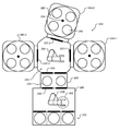
도 3a는 본 개시의 원리들에 따른 예시적인 로드록 및 카메라이다.
도 3b는 본 개시의 원리들에 따른 예시적인 로드록 및 카메라의 또 다른 도면이다.
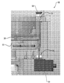
도 3c는 본 개시의 원리들에 따라 캡처된 웨이퍼의 예시적인 이미지이다.
도 4는 본 개시의 원리들에 따른 예시적인 웨이퍼 정렬 방법의 단계들을 예시한다.
도 5는 본 개시의 원리들에 따른 예시적인 웨이퍼 정렬 시스템의 기능적 블록도이다.
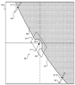
도 6a는 본 개시의 원리들에 따른 테스트 웨이퍼의 예시적인 캘리브레이팅된 이미지이다.
도 6b는 본 개시의 원리들에 따라 오정렬된 웨이퍼의 예시적인 이미지이다.
도 6c는 본 개시의 원리들에 따라 캘리브레이팅된 이미지 및 오정렬된 웨이퍼의 이미지의 예시적인 비교예이다.
도면들에서, 참조 번호들은 유사하고 그리고/또는 동일한 엘리먼트들을 식별하기 위해 재사용될 수도 있다.
Claims (20)
- 페데스탈 상에 위치된 웨이퍼의 이미지를 캡처하는 이미지 캡처 디바이스;
상기 웨이퍼의 에지 및 상기 웨이퍼의 상기 에지에 형성된 노치를 검출하도록 상기 이미지를 분석하고, 그리고 상기 노치의 위치에 기초하여, 상기 웨이퍼의 상기 에지에 대응하는 제 1 에지 위치 및 제 2 에지 위치를 계산하는, 이미지 분석 모듈;
상기 제 1 에지 위치 및 상기 제 2 에지 위치에 기초하여 상기 웨이퍼의 각도 오프셋 (angular offset) 을 계산하는 오프셋 계산 모듈; 및
상기 각도 오프셋에 기초하여 상기 페데스탈로부터 프로세스 셀로 상기 웨이퍼의 이송을 제어하는 시스템 제어 모듈을 포함하는, 웨이퍼 정렬 시스템. - 제 1 항에 있어서,
상기 제 1 에지 위치 및 상기 제 2 에지 위치는 상기 노치의 상기 위치로부터 미리 결정된 거리인, 웨이퍼 정렬 시스템. - 제 1 항에 있어서,
상기 각도 오프셋을 계산하기 위해, 상기 오프셋 계산 모듈은 상기 제 1 에지 위치 및 상기 제 2 에지 위치를 제 3 에지 위치 및 제 4 에지 위치와 비교하는, 웨이퍼 정렬 시스템. - 제 3 항에 있어서,
상기 각도 오프셋은 상기 제 1 에지 위치와 상기 제 3 에지 위치 간의 차 및 상기 제 2 에지 위치와 상기 제 4 에지 위치 간의 차에 대응하는, 웨이퍼 정렬 시스템. - 제 3 항에 있어서,
상기 제 3 에지 위치 및 상기 제 4 에지 위치는 테스트 웨이퍼의 에지에 대응하는, 웨이퍼 정렬 시스템. - 제 5 항에 있어서,
상기 이미지 분석 모듈은, 상기 테스트 웨이퍼가 상기 페데스탈 상의 기준 위치에 배치되는 동안, 캡처된 이미지를 사용하여 상기 제 3 에지 위치 및 상기 제 4 에지 위치를 계산하는, 웨이퍼 정렬 시스템. - 제 5 항에 있어서,
상기 제 1 에지 위치, 상기 제 2 에지 위치, 상기 제 3 에지 위치, 및 상기 제 4 에지 위치 각각은 상기 이미지 캡처 디바이스의 시야 (field of view) 내 좌표들에 대응하는, 웨이퍼 정렬 시스템. - 제 5 항에 있어서,
상기 이미지 캡처 디바이스 반대편의 상기 웨이퍼의 측면 상에 배치된 광원을 더 포함하고, 상기 광원은 상기 이미지 캡처 디바이스를 향해 상기 웨이퍼를 지나서 광을 투사하도록 배치되는, 웨이퍼 정렬 시스템. - 제 8 항에 있어서,
상기 광원은 상기 이미지 캡처 디바이스의 시야를 비추도록 (illuminate) 배치되는, 웨이퍼 정렬 시스템. - 제 1 항에 있어서,
상기 시스템 제어 모듈은 상기 웨이퍼를 상기 프로세스 셀로 이송하기 전에 상기 각도 오프셋에 기초하여 상기 프로세스 셀의 로딩 위치를 조정하는, 웨이퍼 정렬 시스템. - 페데스탈 상에 위치된 웨이퍼의 이미지를 캡처하는 단계;
상기 웨이퍼의 에지 및 상기 웨이퍼의 상기 에지 내에 형성된 노치를 검출하도록 상기 이미지를 분석하는 단계;
상기 노치의 위치에 기초하여, 상기 웨이퍼의 에지에 대응하는 제 1 에지 위치 및 제 2 에지 위치를 계산하는 단계;
상기 제 1 에지 위치 및 상기 제 2 에지 위치에 기초하여 상기 웨이퍼의 각도 오프셋을 계산하는 단계; 및
상기 각도 오프셋에 기초하여 상기 페데스탈로부터 프로세스 셀로 상기 웨이퍼의 이송을 제어하는 단계를 포함하는, 웨이퍼 정렬 방법. - 제 11 항에 있어서,
상기 제 1 에지 위치 및 상기 제 2 에지 위치는 상기 노치의 상기 위치로부터 미리 결정된 거리인, 웨이퍼 정렬 방법. - 제 11 항에 있어서,
상기 각도 오프셋을 계산하는 단계는 상기 제 1 에지 위치 및 상기 제 2 에지 위치를 제 3 에지 위치 및 제 4 에지 위치와 비교하는 단계를 포함하는, 웨이퍼 정렬 방법. - 제 13 항에 있어서,
상기 각도 오프셋은 상기 제 1 에지 위치와 상기 제 3 에지 위치 간의 차 및 상기 제 2 에지 위치와 상기 제 4 에지 위치 간의 차에 대응하는, 웨이퍼 정렬 방법. - 제 13 항에 있어서,
상기 제 3 에지 위치 및 상기 제 4 에지 위치는 테스트 웨이퍼의 에지에 대응하는, 웨이퍼 정렬 방법. - 제 15 항에 있어서,
상기 테스트 웨이퍼가 상기 페데스탈 상의 기준 위치에 배치되는 동안 캡처된 이미지를 사용하여 상기 제 3 에지 위치 및 상기 제 4 에지 위치를 계산하는 단계를 더 포함하는, 웨이퍼 정렬 방법. - 제 15 항에 있어서,
상기 제 1 에지 위치, 상기 제 2 에지 위치, 상기 제 3 에지 위치, 및 상기 제 4 에지 위치 각각은 상기 이미지 캡처 디바이스의 시야 내의 좌표들에 대응하는, 웨이퍼 정렬 방법. - 제 15 항에 있어서,
상기 이미지 캡처 디바이스 반대편의 상기 웨이퍼의 측면 상에 배치된 광원을 사용하여, 상기 이미지 캡처 디바이스를 향해 상기 웨이퍼를 지나 광을 투사하는 단계를 더 포함하는, 웨이퍼 정렬 방법. - 제 18 항에 있어서,
상기 광원은 상기 이미지 캡처 디바이스의 시야를 비추도록 배치되는, 웨이퍼 정렬 방법. - 제 11 항에 있어서,
상기 웨이퍼를 상기 프로세스 셀로 이송하기 전에 상기 각도 오프셋에 기초하여 상기 프로세스 셀의 로딩 위치를 조정하는 단계를 더 포함하는, 웨이퍼 정렬 방법.
Applications Claiming Priority (2)
| Application Number | Priority Date | Filing Date | Title |
|---|---|---|---|
| US14/813,948 US9831110B2 (en) | 2015-07-30 | 2015-07-30 | Vision-based wafer notch position measurement |
| US14/813,948 | 2015-07-30 |
Publications (2)
| Publication Number | Publication Date |
|---|---|
| KR20170015209A true KR20170015209A (ko) | 2017-02-08 |
| KR102662003B1 KR102662003B1 (ko) | 2024-04-29 |
Family
ID=58161295
Family Applications (1)
| Application Number | Title | Priority Date | Filing Date |
|---|---|---|---|
| KR1020160095905A Active KR102662003B1 (ko) | 2015-07-30 | 2016-07-28 | 영상 기반 웨이퍼 노치 위치 측정 |
Country Status (2)
| Country | Link |
|---|---|
| KR (1) | KR102662003B1 (ko) |
| CN (2) | CN106409741B (ko) |
Cited By (9)
| Publication number | Priority date | Publication date | Assignee | Title |
|---|---|---|---|---|
| WO2018143631A1 (ko) | 2017-02-02 | 2018-08-09 | 주식회사 케이티 | 액세스 제어 방법 및 장치 |
| US10665490B2 (en) | 2018-07-04 | 2020-05-26 | Samsung Electronics Co., Ltd. | Apparatus and methods for edge ring replacement, inspection and alignment using image sensors |
| KR20210031805A (ko) * | 2019-09-13 | 2021-03-23 | 브룩스 오토메이션 인코퍼레이티드 | 기판 정렬을 위한 방법 및 장치 |
| KR20210134828A (ko) * | 2019-03-29 | 2021-11-10 | 램 리써치 코포레이션 | 인덱싱된 (indexed) 멀티-스테이션 프로세싱 챔버들 내에서 웨이퍼 배치 보정 |
| WO2022220920A1 (en) * | 2021-04-15 | 2022-10-20 | Jnk Tech | Substrate inspection system and method of use thereof |
| KR20220143165A (ko) * | 2017-12-06 | 2022-10-24 | 램 리써치 코포레이션 | 웨이퍼를 스핀하는 프로세스 모듈의 스테이션에 대한 자동-캘리브레이션 |
| US11840762B2 (en) | 2021-04-15 | 2023-12-12 | Jnk Tech | Substrate inspection system and a method of use thereof |
| CN117259144A (zh) * | 2023-11-20 | 2023-12-22 | 常州铭赛机器人科技股份有限公司 | 晶圆围坝涂胶控制方法、设备及其介质 |
| US12341040B2 (en) | 2019-07-26 | 2025-06-24 | Lam Research Corporation | Integrated adaptive positioning systems and routines for automated wafer-handling robot teach and health check |
Families Citing this family (8)
| Publication number | Priority date | Publication date | Assignee | Title |
|---|---|---|---|---|
| US10338006B2 (en) * | 2017-06-15 | 2019-07-02 | Asm Technology Singapore Pte Ltd | Method and apparatus for aligning and inspecting electronic components |
| CN111146102A (zh) * | 2018-11-02 | 2020-05-12 | 睿励科学仪器(上海)有限公司 | 用于测量晶片的设备和方法 |
| CN112683323B (zh) * | 2020-12-27 | 2024-01-12 | 富联裕展科技(深圳)有限公司 | 检测装置、控制系统及控制方法 |
| CN114293250B (zh) * | 2021-12-29 | 2023-01-06 | 西安奕斯伟材料科技有限公司 | 对硅片位置进行调准的系统、方法及外延设备 |
| CN114322853B (zh) * | 2021-12-31 | 2023-07-25 | 上海果纳半导体技术有限公司 | 气浮平台动态水平度检测方法及应用该方法的晶圆传输系统 |
| CN115241095B (zh) * | 2022-07-29 | 2025-08-26 | 北京北方华创微电子装备有限公司 | 晶圆位置异常检测系统、方法及半导体设备 |
| CN115881568B (zh) * | 2022-11-24 | 2026-03-27 | 苏州华兴源创科技股份有限公司 | 晶圆定位的补偿值测算方法、装置及晶圆定位补偿系统 |
| GB2633768A (en) * | 2023-09-19 | 2025-03-26 | Diodes Inc | Semiconductor manufacturing tool alignment device |
Citations (4)
| Publication number | Priority date | Publication date | Assignee | Title |
|---|---|---|---|---|
| KR100405398B1 (ko) * | 1995-07-14 | 2004-03-30 | 가부시키가이샤 니콘 | 기판의위치결정방법 |
| KR20060088817A (ko) * | 2005-01-28 | 2006-08-07 | 가부시키가이샤 이빔 | 기판처리장치 및 기판처리방법 |
| KR20070048650A (ko) * | 2004-08-31 | 2007-05-09 | 가부시키가이샤 니콘 | 위치 맞춤 방법, 처리 시스템, 기판의 투입 재현성 계측방법, 위치 계측 방법, 노광 방법, 기판 처리 장치, 계측방법 및 계측 장치 |
| KR20140065376A (ko) * | 2011-02-25 | 2014-05-29 | 가부시키가이샤 니콘 | 관찰 장치, 검사 장치, 반도체 장치의 제조 방법, 및 기판 지지 부재 |
Family Cites Families (9)
| Publication number | Priority date | Publication date | Assignee | Title |
|---|---|---|---|---|
| US5905850A (en) * | 1996-06-28 | 1999-05-18 | Lam Research Corporation | Method and apparatus for positioning substrates |
| US7008802B2 (en) * | 2001-05-29 | 2006-03-07 | Asm America, Inc. | Method and apparatus to correct water drift |
| CN1260800C (zh) * | 2001-09-19 | 2006-06-21 | 奥林巴斯光学工业株式会社 | 半导体晶片检查设备 |
| US7233841B2 (en) * | 2002-04-19 | 2007-06-19 | Applied Materials, Inc. | Vision system |
| US6900877B2 (en) * | 2002-06-12 | 2005-05-31 | Asm American, Inc. | Semiconductor wafer position shift measurement and correction |
| JP2005268530A (ja) * | 2004-03-18 | 2005-09-29 | Olympus Corp | 半導体ウエハのアライメント装置 |
| CN101154610B (zh) * | 2006-09-25 | 2010-05-12 | 北京北方微电子基地设备工艺研究中心有限责任公司 | 搬运校准装置及应用该装置的晶片传输系统 |
| JP4530011B2 (ja) * | 2007-09-12 | 2010-08-25 | 富士ゼロックス株式会社 | 位置計測システム |
| JP2012209571A (ja) * | 2012-06-15 | 2012-10-25 | Tokyo Seimitsu Co Ltd | ウェーハのエッジ検出装置 |
-
2016
- 2016-07-28 KR KR1020160095905A patent/KR102662003B1/ko active Active
- 2016-07-29 CN CN201610613778.9A patent/CN106409741B/zh active Active
- 2016-07-29 CN CN202210308785.3A patent/CN114914184B/zh active Active
Patent Citations (4)
| Publication number | Priority date | Publication date | Assignee | Title |
|---|---|---|---|---|
| KR100405398B1 (ko) * | 1995-07-14 | 2004-03-30 | 가부시키가이샤 니콘 | 기판의위치결정방법 |
| KR20070048650A (ko) * | 2004-08-31 | 2007-05-09 | 가부시키가이샤 니콘 | 위치 맞춤 방법, 처리 시스템, 기판의 투입 재현성 계측방법, 위치 계측 방법, 노광 방법, 기판 처리 장치, 계측방법 및 계측 장치 |
| KR20060088817A (ko) * | 2005-01-28 | 2006-08-07 | 가부시키가이샤 이빔 | 기판처리장치 및 기판처리방법 |
| KR20140065376A (ko) * | 2011-02-25 | 2014-05-29 | 가부시키가이샤 니콘 | 관찰 장치, 검사 장치, 반도체 장치의 제조 방법, 및 기판 지지 부재 |
Cited By (17)
| Publication number | Priority date | Publication date | Assignee | Title |
|---|---|---|---|---|
| WO2018143631A1 (ko) | 2017-02-02 | 2018-08-09 | 주식회사 케이티 | 액세스 제어 방법 및 장치 |
| KR20230038598A (ko) * | 2017-12-06 | 2023-03-20 | 램 리써치 코포레이션 | 웨이퍼를 스핀하는 프로세스 모듈의 스테이션에 대한 자동-캘리브레이션 |
| KR20220143165A (ko) * | 2017-12-06 | 2022-10-24 | 램 리써치 코포레이션 | 웨이퍼를 스핀하는 프로세스 모듈의 스테이션에 대한 자동-캘리브레이션 |
| US10665490B2 (en) | 2018-07-04 | 2020-05-26 | Samsung Electronics Co., Ltd. | Apparatus and methods for edge ring replacement, inspection and alignment using image sensors |
| KR20210134828A (ko) * | 2019-03-29 | 2021-11-10 | 램 리써치 코포레이션 | 인덱싱된 (indexed) 멀티-스테이션 프로세싱 챔버들 내에서 웨이퍼 배치 보정 |
| US12341040B2 (en) | 2019-07-26 | 2025-06-24 | Lam Research Corporation | Integrated adaptive positioning systems and routines for automated wafer-handling robot teach and health check |
| KR20210031805A (ko) * | 2019-09-13 | 2021-03-23 | 브룩스 오토메이션 인코퍼레이티드 | 기판 정렬을 위한 방법 및 장치 |
| KR20230167765A (ko) * | 2021-04-15 | 2023-12-11 | 제이엔케이 테크 | 기판 검사 시스템 및 그의 사용 방법 |
| US11508590B2 (en) | 2021-04-15 | 2022-11-22 | Jnk Tech | Substrate inspection system and method of use thereof |
| US11840762B2 (en) | 2021-04-15 | 2023-12-12 | Jnk Tech | Substrate inspection system and a method of use thereof |
| US11901202B2 (en) | 2021-04-15 | 2024-02-13 | Jnk Tech | Substrate inspection system and method of use thereof |
| US11987884B2 (en) | 2021-04-15 | 2024-05-21 | Jnk Tech | Glass and wafer inspection system and a method of use thereof |
| US12258665B2 (en) | 2021-04-15 | 2025-03-25 | Jnk Tech | Substrate inspection system and a method of use thereof |
| US12322616B2 (en) | 2021-04-15 | 2025-06-03 | Jnk Tech | Substrate inspection system and method of use thereof |
| WO2022220920A1 (en) * | 2021-04-15 | 2022-10-20 | Jnk Tech | Substrate inspection system and method of use thereof |
| CN117259144A (zh) * | 2023-11-20 | 2023-12-22 | 常州铭赛机器人科技股份有限公司 | 晶圆围坝涂胶控制方法、设备及其介质 |
| CN117259144B (zh) * | 2023-11-20 | 2024-03-12 | 常州铭赛机器人科技股份有限公司 | 晶圆围坝涂胶控制方法、设备及其介质 |
Also Published As
| Publication number | Publication date |
|---|---|
| CN114914184B (zh) | 2025-10-24 |
| CN106409741B (zh) | 2022-04-19 |
| CN106409741A (zh) | 2017-02-15 |
| CN114914184A (zh) | 2022-08-16 |
| KR102662003B1 (ko) | 2024-04-29 |
Similar Documents
| Publication | Publication Date | Title |
|---|---|---|
| KR102662003B1 (ko) | 영상 기반 웨이퍼 노치 위치 측정 | |
| US9831110B2 (en) | Vision-based wafer notch position measurement | |
| US12489006B2 (en) | Auto-calibration to a station of a process module that spins a wafer | |
| CN109983569B (zh) | 使用环动态对准数据的边缘环居中方法 | |
| TW201834139A (zh) | 具有小間隙之銷升降器組件 | |
| TW201740501A (zh) | 晶圓傳送用的晶圓升降環系統 | |
| KR20230145013A (ko) | 깨끗한/더러운 기판 핸들링을 위한 엔드 이펙터 어셈블리 | |
| KR102888626B1 (ko) | 자동화된 회전 사전 정렬을 사용한 에지 링 이송 | |
| JP7608471B2 (ja) | 基板処理システムのための高精度エッジリングのセンタリング | |
| US20240203703A1 (en) | Shadow ring alignment for substrate support | |
| TWI879762B (zh) | 基板處理系統之高精度邊緣環定心 | |
| WO2023081106A1 (en) | Pin lift hard stop | |
| TW202527606A (zh) | 基板處理系統之高精度邊緣環定心 |
Legal Events
| Date | Code | Title | Description |
|---|---|---|---|
| E13-X000 | Pre-grant limitation requested |
St.27 status event code: A-2-3-E10-E13-lim-X000 |
|
| PA0109 | Patent application |
St.27 status event code: A-0-1-A10-A12-nap-PA0109 |
|
| AMND | Amendment | ||
| P11-X000 | Amendment of application requested |
St.27 status event code: A-2-2-P10-P11-nap-X000 |
|
| P13-X000 | Application amended |
St.27 status event code: A-2-2-P10-P13-nap-X000 |
|
| PG1501 | Laying open of application |
St.27 status event code: A-1-1-Q10-Q12-nap-PG1501 |
|
| PA0201 | Request for examination |
St.27 status event code: A-1-2-D10-D11-exm-PA0201 |
|
| E902 | Notification of reason for refusal | ||
| PE0902 | Notice of grounds for rejection |
St.27 status event code: A-1-2-D10-D21-exm-PE0902 |
|
| AMND | Amendment | ||
| P11-X000 | Amendment of application requested |
St.27 status event code: A-2-2-P10-P11-nap-X000 |
|
| P13-X000 | Application amended |
St.27 status event code: A-2-2-P10-P13-nap-X000 |
|
| E601 | Decision to refuse application | ||
| PE0601 | Decision on rejection of patent |
St.27 status event code: N-2-6-B10-B15-exm-PE0601 |
|
| AMND | Amendment | ||
| P11-X000 | Amendment of application requested |
St.27 status event code: A-2-2-P10-P11-nap-X000 |
|
| P13-X000 | Application amended |
St.27 status event code: A-2-2-P10-P13-nap-X000 |
|
| PX0901 | Re-examination |
St.27 status event code: A-2-3-E10-E12-rex-PX0901 |
|
| PX0701 | Decision of registration after re-examination |
St.27 status event code: A-3-4-F10-F13-rex-PX0701 |
|
| X701 | Decision to grant (after re-examination) | ||
| GRNT | Written decision to grant | ||
| PR0701 | Registration of establishment |
St.27 status event code: A-2-4-F10-F11-exm-PR0701 |
|
| PR1002 | Payment of registration fee |
St.27 status event code: A-2-2-U10-U11-oth-PR1002 Fee payment year number: 1 |
|
| PG1601 | Publication of registration |
St.27 status event code: A-4-4-Q10-Q13-nap-PG1601 |
|
| P22-X000 | Classification modified |
St.27 status event code: A-4-4-P10-P22-nap-X000 |