KR20170016007A - 리소그래피 장치, 기판을 이송하는 방법 및 디바이스 제조 방법 - Google Patents
리소그래피 장치, 기판을 이송하는 방법 및 디바이스 제조 방법 Download PDFInfo
- Publication number
- KR20170016007A KR20170016007A KR1020177001213A KR20177001213A KR20170016007A KR 20170016007 A KR20170016007 A KR 20170016007A KR 1020177001213 A KR1020177001213 A KR 1020177001213A KR 20177001213 A KR20177001213 A KR 20177001213A KR 20170016007 A KR20170016007 A KR 20170016007A
- Authority
- KR
- South Korea
- Prior art keywords
- substrate
- drying station
- liquid
- exposure
- post
- Prior art date
- Legal status (The legal status is an assumption and is not a legal conclusion. Google has not performed a legal analysis and makes no representation as to the accuracy of the status listed.)
- Granted
Links
Images





Classifications
-
- G—PHYSICS
- G03—PHOTOGRAPHY; CINEMATOGRAPHY; ANALOGOUS TECHNIQUES USING WAVES OTHER THAN OPTICAL WAVES; ELECTROGRAPHY; HOLOGRAPHY
- G03F—PHOTOMECHANICAL PRODUCTION OF TEXTURED OR PATTERNED SURFACES, e.g. FOR PRINTING, FOR PROCESSING OF SEMICONDUCTOR DEVICES; MATERIALS THEREFOR; ORIGINALS THEREFOR; APPARATUS SPECIALLY ADAPTED THEREFOR
- G03F7/00—Photomechanical, e.g. photolithographic, production of textured or patterned surfaces, e.g. printing surfaces; Materials therefor, e.g. comprising photoresists; Apparatus specially adapted therefor
- G03F7/70—Microphotolithographic exposure; Apparatus therefor
- G03F7/70216—Mask projection systems
- G03F7/70341—Details of immersion lithography aspects, e.g. exposure media or control of immersion liquid supply
-
- H—ELECTRICITY
- H10—SEMICONDUCTOR DEVICES; ELECTRIC SOLID-STATE DEVICES NOT OTHERWISE PROVIDED FOR
- H10P—GENERIC PROCESSES OR APPARATUS FOR THE MANUFACTURE OR TREATMENT OF DEVICES COVERED BY CLASS H10
- H10P72/00—Handling or holding of wafers, substrates or devices during manufacture or treatment thereof
- H10P72/04—Apparatus for manufacture or treatment
- H10P72/0402—Apparatus for fluid treatment
- H10P72/0406—Apparatus for fluid treatment for cleaning followed by drying, rinsing, stripping, blasting or the like
- H10P72/0408—Apparatus for fluid treatment for cleaning followed by drying, rinsing, stripping, blasting or the like for drying
-
- G—PHYSICS
- G03—PHOTOGRAPHY; CINEMATOGRAPHY; ANALOGOUS TECHNIQUES USING WAVES OTHER THAN OPTICAL WAVES; ELECTROGRAPHY; HOLOGRAPHY
- G03F—PHOTOMECHANICAL PRODUCTION OF TEXTURED OR PATTERNED SURFACES, e.g. FOR PRINTING, FOR PROCESSING OF SEMICONDUCTOR DEVICES; MATERIALS THEREFOR; ORIGINALS THEREFOR; APPARATUS SPECIALLY ADAPTED THEREFOR
- G03F7/00—Photomechanical, e.g. photolithographic, production of textured or patterned surfaces, e.g. printing surfaces; Materials therefor, e.g. comprising photoresists; Apparatus specially adapted therefor
- G03F7/16—Coating processes; Apparatus therefor
- G03F7/168—Finishing the coated layer, e.g. drying, baking, soaking
-
- G—PHYSICS
- G03—PHOTOGRAPHY; CINEMATOGRAPHY; ANALOGOUS TECHNIQUES USING WAVES OTHER THAN OPTICAL WAVES; ELECTROGRAPHY; HOLOGRAPHY
- G03F—PHOTOMECHANICAL PRODUCTION OF TEXTURED OR PATTERNED SURFACES, e.g. FOR PRINTING, FOR PROCESSING OF SEMICONDUCTOR DEVICES; MATERIALS THEREFOR; ORIGINALS THEREFOR; APPARATUS SPECIALLY ADAPTED THEREFOR
- G03F7/00—Photomechanical, e.g. photolithographic, production of textured or patterned surfaces, e.g. printing surfaces; Materials therefor, e.g. comprising photoresists; Apparatus specially adapted therefor
- G03F7/70—Microphotolithographic exposure; Apparatus therefor
- G03F7/70691—Handling of masks or workpieces
- G03F7/70733—Handling masks and workpieces, e.g. exchange of workpiece or mask, transport of workpiece or mask
-
- G—PHYSICS
- G03—PHOTOGRAPHY; CINEMATOGRAPHY; ANALOGOUS TECHNIQUES USING WAVES OTHER THAN OPTICAL WAVES; ELECTROGRAPHY; HOLOGRAPHY
- G03F—PHOTOMECHANICAL PRODUCTION OF TEXTURED OR PATTERNED SURFACES, e.g. FOR PRINTING, FOR PROCESSING OF SEMICONDUCTOR DEVICES; MATERIALS THEREFOR; ORIGINALS THEREFOR; APPARATUS SPECIALLY ADAPTED THEREFOR
- G03F7/00—Photomechanical, e.g. photolithographic, production of textured or patterned surfaces, e.g. printing surfaces; Materials therefor, e.g. comprising photoresists; Apparatus specially adapted therefor
- G03F7/70—Microphotolithographic exposure; Apparatus therefor
- G03F7/70691—Handling of masks or workpieces
- G03F7/70733—Handling masks and workpieces, e.g. exchange of workpiece or mask, transport of workpiece or mask
- G03F7/7075—Handling workpieces outside exposure position, e.g. SMIF box
-
- G—PHYSICS
- G03—PHOTOGRAPHY; CINEMATOGRAPHY; ANALOGOUS TECHNIQUES USING WAVES OTHER THAN OPTICAL WAVES; ELECTROGRAPHY; HOLOGRAPHY
- G03F—PHOTOMECHANICAL PRODUCTION OF TEXTURED OR PATTERNED SURFACES, e.g. FOR PRINTING, FOR PROCESSING OF SEMICONDUCTOR DEVICES; MATERIALS THEREFOR; ORIGINALS THEREFOR; APPARATUS SPECIALLY ADAPTED THEREFOR
- G03F7/00—Photomechanical, e.g. photolithographic, production of textured or patterned surfaces, e.g. printing surfaces; Materials therefor, e.g. comprising photoresists; Apparatus specially adapted therefor
- G03F7/70—Microphotolithographic exposure; Apparatus therefor
- G03F7/708—Construction of apparatus, e.g. environment aspects, hygiene aspects or materials
- G03F7/70808—Construction details, e.g. housing, load-lock, seals or windows for passing light in or out of apparatus
- G03F7/70825—Mounting of individual elements, e.g. mounts, holders or supports
-
- G—PHYSICS
- G03—PHOTOGRAPHY; CINEMATOGRAPHY; ANALOGOUS TECHNIQUES USING WAVES OTHER THAN OPTICAL WAVES; ELECTROGRAPHY; HOLOGRAPHY
- G03F—PHOTOMECHANICAL PRODUCTION OF TEXTURED OR PATTERNED SURFACES, e.g. FOR PRINTING, FOR PROCESSING OF SEMICONDUCTOR DEVICES; MATERIALS THEREFOR; ORIGINALS THEREFOR; APPARATUS SPECIALLY ADAPTED THEREFOR
- G03F7/00—Photomechanical, e.g. photolithographic, production of textured or patterned surfaces, e.g. printing surfaces; Materials therefor, e.g. comprising photoresists; Apparatus specially adapted therefor
- G03F7/70—Microphotolithographic exposure; Apparatus therefor
- G03F7/708—Construction of apparatus, e.g. environment aspects, hygiene aspects or materials
- G03F7/70991—Connection with other apparatus, e.g. multiple exposure stations, particular arrangement of exposure apparatus and pre-exposure and/or post-exposure apparatus; Shared apparatus, e.g. having shared radiation source, shared mask or workpiece stage, shared base-plate; Utilities, e.g. cable, pipe or wireless arrangements for data, power, fluids or vacuum
-
- H01L21/67742—
-
- H01L21/67766—
-
- H01L21/67778—
-
- H—ELECTRICITY
- H10—SEMICONDUCTOR DEVICES; ELECTRIC SOLID-STATE DEVICES NOT OTHERWISE PROVIDED FOR
- H10P—GENERIC PROCESSES OR APPARATUS FOR THE MANUFACTURE OR TREATMENT OF DEVICES COVERED BY CLASS H10
- H10P72/00—Handling or holding of wafers, substrates or devices during manufacture or treatment thereof
- H10P72/04—Apparatus for manufacture or treatment
- H10P72/0402—Apparatus for fluid treatment
- H10P72/0406—Apparatus for fluid treatment for cleaning followed by drying, rinsing, stripping, blasting or the like
- H10P72/0411—Apparatus for fluid treatment for cleaning followed by drying, rinsing, stripping, blasting or the like for wet cleaning or washing
-
- H—ELECTRICITY
- H10—SEMICONDUCTOR DEVICES; ELECTRIC SOLID-STATE DEVICES NOT OTHERWISE PROVIDED FOR
- H10P—GENERIC PROCESSES OR APPARATUS FOR THE MANUFACTURE OR TREATMENT OF DEVICES COVERED BY CLASS H10
- H10P72/00—Handling or holding of wafers, substrates or devices during manufacture or treatment thereof
- H10P72/04—Apparatus for manufacture or treatment
- H10P72/0451—Apparatus for manufacturing or treating in a plurality of work-stations
- H10P72/0452—Apparatus for manufacturing or treating in a plurality of work-stations characterised by the layout of the process chambers
- H10P72/0458—Apparatus for manufacturing or treating in a plurality of work-stations characterised by the layout of the process chambers vertical arrangement
-
- H—ELECTRICITY
- H10—SEMICONDUCTOR DEVICES; ELECTRIC SOLID-STATE DEVICES NOT OTHERWISE PROVIDED FOR
- H10P—GENERIC PROCESSES OR APPARATUS FOR THE MANUFACTURE OR TREATMENT OF DEVICES COVERED BY CLASS H10
- H10P72/00—Handling or holding of wafers, substrates or devices during manufacture or treatment thereof
- H10P72/04—Apparatus for manufacture or treatment
- H10P72/0451—Apparatus for manufacturing or treating in a plurality of work-stations
- H10P72/0468—Apparatus for manufacturing or treating in a plurality of work-stations comprising a chamber adapted to a particular process
-
- H—ELECTRICITY
- H10—SEMICONDUCTOR DEVICES; ELECTRIC SOLID-STATE DEVICES NOT OTHERWISE PROVIDED FOR
- H10P—GENERIC PROCESSES OR APPARATUS FOR THE MANUFACTURE OR TREATMENT OF DEVICES COVERED BY CLASS H10
- H10P72/00—Handling or holding of wafers, substrates or devices during manufacture or treatment thereof
- H10P72/04—Apparatus for manufacture or treatment
- H10P72/0451—Apparatus for manufacturing or treating in a plurality of work-stations
- H10P72/0468—Apparatus for manufacturing or treating in a plurality of work-stations comprising a chamber adapted to a particular process
- H10P72/0474—Apparatus for manufacturing or treating in a plurality of work-stations comprising a chamber adapted to a particular process comprising at least one lithography chamber
-
- H—ELECTRICITY
- H10—SEMICONDUCTOR DEVICES; ELECTRIC SOLID-STATE DEVICES NOT OTHERWISE PROVIDED FOR
- H10P—GENERIC PROCESSES OR APPARATUS FOR THE MANUFACTURE OR TREATMENT OF DEVICES COVERED BY CLASS H10
- H10P72/00—Handling or holding of wafers, substrates or devices during manufacture or treatment thereof
- H10P72/30—Handling or holding of wafers, substrates or devices during manufacture or treatment thereof for conveying, e.g. between different workstations
- H10P72/33—Handling or holding of wafers, substrates or devices during manufacture or treatment thereof for conveying, e.g. between different workstations into and out of processing chamber
- H10P72/3302—Mechanical parts of transfer devices
-
- H—ELECTRICITY
- H10—SEMICONDUCTOR DEVICES; ELECTRIC SOLID-STATE DEVICES NOT OTHERWISE PROVIDED FOR
- H10P—GENERIC PROCESSES OR APPARATUS FOR THE MANUFACTURE OR TREATMENT OF DEVICES COVERED BY CLASS H10
- H10P72/00—Handling or holding of wafers, substrates or devices during manufacture or treatment thereof
- H10P72/30—Handling or holding of wafers, substrates or devices during manufacture or treatment thereof for conveying, e.g. between different workstations
- H10P72/34—Handling or holding of wafers, substrates or devices during manufacture or treatment thereof for conveying, e.g. between different workstations the wafers being stored in a carrier, involving loading and unloading
- H10P72/3402—Mechanical parts of transfer devices
-
- H—ELECTRICITY
- H10—SEMICONDUCTOR DEVICES; ELECTRIC SOLID-STATE DEVICES NOT OTHERWISE PROVIDED FOR
- H10P—GENERIC PROCESSES OR APPARATUS FOR THE MANUFACTURE OR TREATMENT OF DEVICES COVERED BY CLASS H10
- H10P72/00—Handling or holding of wafers, substrates or devices during manufacture or treatment thereof
- H10P72/30—Handling or holding of wafers, substrates or devices during manufacture or treatment thereof for conveying, e.g. between different workstations
- H10P72/34—Handling or holding of wafers, substrates or devices during manufacture or treatment thereof for conveying, e.g. between different workstations the wafers being stored in a carrier, involving loading and unloading
- H10P72/3411—Handling or holding of wafers, substrates or devices during manufacture or treatment thereof for conveying, e.g. between different workstations the wafers being stored in a carrier, involving loading and unloading involving loading and unloading of wafers
-
- H—ELECTRICITY
- H10—SEMICONDUCTOR DEVICES; ELECTRIC SOLID-STATE DEVICES NOT OTHERWISE PROVIDED FOR
- H10W—GENERIC PACKAGES, INTERCONNECTIONS, CONNECTORS OR OTHER CONSTRUCTIONAL DETAILS OF DEVICES COVERED BY CLASS H10
- H10W72/00—Interconnections or connectors in packages
- H10W72/071—Connecting or disconnecting
Landscapes
- Physics & Mathematics (AREA)
- General Physics & Mathematics (AREA)
- Engineering & Computer Science (AREA)
- Health & Medical Sciences (AREA)
- Environmental & Geological Engineering (AREA)
- Epidemiology (AREA)
- Public Health (AREA)
- Computer Networks & Wireless Communication (AREA)
- Exposure And Positioning Against Photoresist Photosensitive Materials (AREA)
- Container, Conveyance, Adherence, Positioning, Of Wafer (AREA)
- Robotics (AREA)
Abstract
Description
도 1은 본 발명의 일 실시예에 따른 리소그래피 장치를 도시하는 도면;
도 2는 본 발명의 일 실시예에 따른 리소그래피 장치의 일부분을 도시하는 도면;
도 3은 본 발명의 일 실시예에 따른 리소그래피 장치의 일부분을 도시하는 도면;
도 4 및 도 5는 본 발명의 일 실시예에 따른 리소그래피 장치의 일부분을 도시하는 도면;
도 6 내지 도 8은 본 발명의 일 실시예에 따른 리소그래피 장치를 개략적으로 도시하는 도면;
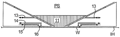
도 9 내지 도 14는 본 발명의 일 실시예에 따른 리소그래피 장치의 일부분을 도시하는 도면; 및
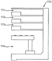
도 15 및 도 16은 각각 본 발명의 일 실시예에 따른 건조 스테이션을 도시하는 도면이다.


Claims (15)
- 리소그래피 장치에 있어서,
노광 공정을 위해 기판을 지지하도록 구성되는 기판 테이블 - 상기 노광 공정에서 상기 기판은 액체를 통해 패턴을 형성하도록 방사선 빔에 노광됨 -;
기판 후-노광(substrate post-exposure)을 핸들링(handle)하는 후-노광 핸들링 모듈 - 상기 후-노광 핸들링 모듈은 저장 유닛을 포함하고, 상기 저장 유닛은 상기 저장 유닛의 각각의 기판 수용 유닛(substrate accommodation unit)들에 복수의 기판들을 저장하도록 구성됨 -;
상기 기판 테이블로부터 기판 언로딩 경로(substrate unloading path)를 따라 상기 후-노광 핸들링 모듈 내로 상기 기판을 이송하도록 구성되는 기판 핸들링 로봇; 및
상기 기판의 표면으로부터 액체를 능동적으로(actively) 제거하도록 구성되는 건조 스테이션을 포함하고,
상기 건조 스테이션은 상기 저장 유닛에 위치되는 리소그래피 장치. - 제 1 항에 있어서,
상기 후-노광 핸들링 모듈은 기판 핸들러인 리소그래피 장치. - 제 1 항 또는 제 2 항에 있어서,
상기 기판 핸들링 로봇은 위치설정기 부분(positioner part) 및 상기 위치설정기 부분과 인터페이싱(interface)하는 홀더를 포함하고, 상기 홀더는 상기 기판을 유지하도록 구성되며, 상기 위치설정기 부분은 상기 홀더가 상기 기판 테이블 상에 상기 기판을 유지하는 로봇 언로드 위치와 상기 홀더가 상기 후-노광 핸들링 모듈에 상기 기판을 유지하는 로봇 핸들링 위치 사이에서 이동하도록 구성되는 리소그래피 장치. - 제 1 항 내지 제 3 항 중 어느 한 항에 있어서,
상기 후-노광 핸들링 모듈은 상기 기판 핸들링 로봇과 연계된 파라미터를 측정하도록 구성되는 적어도 하나의 기판 핸들러 센서를 포함하고, 상기 적어도 하나의 기판 핸들러 센서는 상기 기판 언로딩 경로에 위치되는 리소그래피 장치. - 제 1 항 내지 제 4 항 중 어느 한 항에 있어서,
상기 건조 스테이션은, 상기 기판의 표면으로부터 액체를 능동적으로 제거하도록 구성되는 건조 스테이션 아암(drying station arm), 및 상기 기판의 표면과 평행한 회전 평면을 통해 상기 건조 스테이션 아암을 회전시키도록 구성되는 로테이터(rotator)의 형태를 갖는 리소그래피 장치. - 제 1 항 내지 제 5 항 중 어느 한 항에 있어서,
상기 기판을 회전시키도록 구성되는 기판 턴테이블(substrate turntable)을 더 포함하고, 상기 건조 스테이션은 상기 기판 턴테이블의 반경에 걸쳐 연장되는 건조 스테이션 아암의 형태를 가져, 상기 기판이 상기 기판 턴테이블 상에서 회전될 때, 상기 건조 스테이션 아암은 상기 기판의 표면으로부터 액체를 능동적으로 제거하도록 구성되는 리소그래피 장치. - 제 1 항 내지 제 6 항 중 어느 한 항에 있어서,
상기 건조 스테이션은, 상기 기판이 상기 기판 테이블로부터 언로딩되는 기판 언로드 위치 부근에 위치되는 리소그래피 장치. - 제 1 항 내지 제 7 항 중 어느 한 항에 있어서,
상기 건조 스테이션은, 상기 건조 스테이션이 상기 기판의 표면으로부터 액체를 능동적으로 제거하는 건조 위치와 비-건조 위치 사이에서 상기 건조 스테이션을 상기 기판에 대해 위아래로 이동시키도록 구성되는 건조 스테이션 액추에이터를 포함하는 리소그래피 장치. - 제 1 항 내지 제 8 항 중 어느 한 항에 있어서,
상기 건조 스테이션은 가스 나이프, 워터 배스(water bath) 및 액체 연속 유동(continuous flow of liquid) 중 하나 이상을 포함하는 리소그래피 장치. - 리소그래피 장치에서 기판을 이송하는 방법에 있어서,
노광 공정을 위해 기판을 지지하는 단계 - 상기 노광 공정에서 상기 기판은 액체를 통해 패턴을 형성하도록 방사선 빔에 노광됨 -;
기판 언로딩 경로를 따라 기판 후-노광을 핸들링하는 후-노광 핸들링 모듈 내로 상기 기판을 이송하는 단계 - 상기 후-노광 핸들링 모듈은 저장 유닛을 포함하고, 상기 저장 유닛은 상기 저장 유닛의 각각의 기판 수용 유닛들에 복수의 기판들을 저장하도록 구성됨 -; 및
상기 기판의 표면으로부터 액체를 능동적으로 제거하는 단계를 포함하고,
상기 액체의 능동 제거는 상기 저장 유닛에서 수행되는 기판 이송 방법. - 제 10 항에 있어서,
상기 후-노광 핸들링 모듈은 상기 기판 핸들링 로봇과 연계된 파라미터를 측정하도록 구성되는 적어도 하나의 기판 핸들러 센서를 포함하고, 상기 적어도 하나의 기판 핸들러 센서는 상기 기판 언로딩 경로에 위치되는 기판 이송 방법. - 제 10 항 또는 제 11 항에 있어서,
상기 기판의 표면으로부터 액체를 능동적으로 제거하기 위해, 상기 기판의 표면에 평행한 회전 평면을 통해 건조 스테이션 아암을 회전시키는 단계를 더 포함하는 기판 이송 방법. - 제 10 항 내지 제 12 항 중 어느 한 항에 있어서,
상기 기판을 회전시키는 단계를 포함하고, 상기 액체의 능동 제거는 기판 턴테이블의 반경에 걸쳐 연장되는 건조 스테이션 아암에 의해 수행되어, 상기 기판이 회전될 때, 상기 건조 스테이션 아암은 상기 기판의 표면으로부터 액체를 능동적으로 제거하는 기판 이송 방법. - 제 10 항 내지 제 13 항 중 어느 한 항에 있어서,
상기 건조 스테이션이 상기 기판의 표면으로부터 액체를 능동적으로 제거하는 건조 위치와 비-건조 위치 사이에서 상기 액체의 능동 제거를 수행하는 건조 스테이션을 상기 기판에 대해 위아래로 이동시키는 단계를 더 포함하는 기판 이송 방법. - 제 10 항 내지 제 14 항 중 어느 한 항에 있어서,
상기 액체의 능동 제거는 가스 나이프, 워터 배스 및 액체 연속 유동 중 하나 이상을 이용하여 수행되는 기판 이송 방법.
Applications Claiming Priority (7)
| Application Number | Priority Date | Filing Date | Title |
|---|---|---|---|
| EP14172626.5 | 2014-06-16 | ||
| EP14172626 | 2014-06-16 | ||
| EP14178554 | 2014-07-25 | ||
| EP14178554.3 | 2014-07-25 | ||
| EP14198779 | 2014-12-18 | ||
| EP14198779.2 | 2014-12-18 | ||
| PCT/EP2015/060427 WO2015193036A1 (en) | 2014-06-16 | 2015-05-12 | Lithographic apparatus, method of transferring a substrate and device manufacturing method |
Publications (2)
| Publication Number | Publication Date |
|---|---|
| KR20170016007A true KR20170016007A (ko) | 2017-02-10 |
| KR101941596B1 KR101941596B1 (ko) | 2019-01-23 |
Family
ID=53199963
Family Applications (1)
| Application Number | Title | Priority Date | Filing Date |
|---|---|---|---|
| KR1020177001213A Active KR101941596B1 (ko) | 2014-06-16 | 2015-05-12 | 리소그래피 장치, 기판을 이송하는 방법 및 디바이스 제조 방법 |
Country Status (10)
| Country | Link |
|---|---|
| US (2) | US10409174B2 (ko) |
| EP (1) | EP3155482B1 (ko) |
| JP (2) | JP6251825B2 (ko) |
| KR (1) | KR101941596B1 (ko) |
| CN (2) | CN106507684B (ko) |
| IL (1) | IL249047A0 (ko) |
| NL (1) | NL2014792A (ko) |
| SG (1) | SG11201609642QA (ko) |
| TW (2) | TWI647544B (ko) |
| WO (1) | WO2015193036A1 (ko) |
Cited By (1)
| Publication number | Priority date | Publication date | Assignee | Title |
|---|---|---|---|---|
| KR20200056515A (ko) * | 2018-11-14 | 2020-05-25 | 삼성전자주식회사 | 기판 건조 방법, 포토레지스트 현상 방법, 그들을 포함하는 포토리소그래피 방법, 및 기판 건조 장치 |
Families Citing this family (6)
| Publication number | Priority date | Publication date | Assignee | Title |
|---|---|---|---|---|
| CN105717754A (zh) * | 2016-04-07 | 2016-06-29 | 上海华力微电子有限公司 | 一种显影装置及使用该显影装置降低水渍缺陷的方法 |
| JP6892727B2 (ja) * | 2016-09-26 | 2021-06-23 | カンタツ株式会社 | パターン製造装置、パターン製造方法およびパターン製造プログラム |
| SG11201906413XA (en) * | 2017-02-03 | 2019-08-27 | Asml Netherlands Bv | Exposure apparatus |
| EP3764165A1 (en) | 2019-07-12 | 2021-01-13 | ASML Netherlands B.V. | Substrate shape measuring device |
| WO2021094057A1 (en) | 2019-11-14 | 2021-05-20 | Asml Netherlands B.V. | Substrate support, lithographic apparatus, method for manipulating charge distribution and method for preparing a substrate |
| US12287581B2 (en) | 2021-05-28 | 2025-04-29 | Taiwan Semiconductor Manufacturing Company, Ltd. | Method of manufacturing semiconductor devices using a photomask |
Citations (3)
| Publication number | Priority date | Publication date | Assignee | Title |
|---|---|---|---|---|
| KR100540365B1 (ko) * | 1999-04-21 | 2006-01-10 | 에이에스엠엘 네델란즈 비.브이. | 리소그래피투영 장치의 마스크-핸들링 장치 |
| KR100760317B1 (ko) * | 2004-08-13 | 2007-09-20 | 에이에스엠엘 네델란즈 비.브이. | 리소그래피 장치 및 디바이스 제조방법 |
| KR20090028421A (ko) * | 2007-09-13 | 2009-03-18 | 가부시키가이샤 소쿠도 | 기판처리장치 및 기판처리방법 |
Family Cites Families (40)
| Publication number | Priority date | Publication date | Assignee | Title |
|---|---|---|---|---|
| US5874820A (en) | 1995-04-04 | 1999-02-23 | Nikon Corporation | Window frame-guided stage mechanism |
| JP2001308003A (ja) | 2000-02-15 | 2001-11-02 | Nikon Corp | 露光方法及び装置、並びにデバイス製造方法 |
| JP2002305140A (ja) | 2001-04-06 | 2002-10-18 | Nikon Corp | 露光装置及び基板処理システム |
| US20030012631A1 (en) * | 2001-07-12 | 2003-01-16 | Pencis Christopher H. | High temperature substrate transfer robot |
| SG135052A1 (en) | 2002-11-12 | 2007-09-28 | Asml Netherlands Bv | Lithographic apparatus and device manufacturing method |
| EP1420298B1 (en) | 2002-11-12 | 2013-02-20 | ASML Netherlands B.V. | Lithographic apparatus |
| US7384484B2 (en) | 2002-11-18 | 2008-06-10 | Dainippon Screen Mfg. Co., Ltd. | Substrate processing method, substrate processing apparatus and substrate processing system |
| WO2004053952A1 (ja) | 2002-12-10 | 2004-06-24 | Nikon Corporation | 露光装置及びデバイス製造方法 |
| WO2004102646A1 (ja) | 2003-05-15 | 2004-11-25 | Nikon Corporation | 露光装置及びデバイス製造方法 |
| TWI474380B (zh) | 2003-05-23 | 2015-02-21 | 尼康股份有限公司 | A method of manufacturing an exposure apparatus and an element |
| US7070915B2 (en) * | 2003-08-29 | 2006-07-04 | Tokyo Electron Limited | Method and system for drying a substrate |
| KR20060126949A (ko) | 2003-10-08 | 2006-12-11 | 가부시키가이샤 니콘 | 기판 반송 장치와 기판 반송 방법, 노광 장치와 노광 방법,및 디바이스 제조 방법 |
| JP2005136364A (ja) * | 2003-10-08 | 2005-05-26 | Zao Nikon Co Ltd | 基板搬送装置、露光装置、並びにデバイス製造方法 |
| US7927429B2 (en) | 2003-11-18 | 2011-04-19 | Tokyo Electron Limited | Substrate cleaning method, substrate cleaning apparatus and computer readable recording medium |
| US7616383B2 (en) | 2004-05-18 | 2009-11-10 | Asml Netherlands B.V. | Lithographic apparatus and device manufacturing method |
| JP2006080143A (ja) | 2004-09-07 | 2006-03-23 | Matsushita Electric Ind Co Ltd | 露光装置及びパターン形成方法 |
| JP4324527B2 (ja) | 2004-09-09 | 2009-09-02 | 東京エレクトロン株式会社 | 基板洗浄方法及び現像装置 |
| WO2006038472A1 (ja) * | 2004-10-06 | 2006-04-13 | Ebara Corporation | 基板処理装置及び基板処理方法 |
| JP2006310724A (ja) | 2004-11-10 | 2006-11-09 | Dainippon Screen Mfg Co Ltd | 基板処理装置および基板処理方法 |
| US7446850B2 (en) * | 2004-12-03 | 2008-11-04 | Asml Netherlands B.V. | Lithographic apparatus and device manufacturing method |
| CN100535757C (zh) * | 2004-12-06 | 2009-09-02 | 株式会社迅动 | 基板处理装置 |
| US8211242B2 (en) | 2005-02-07 | 2012-07-03 | Ebara Corporation | Substrate processing method, substrate processing apparatus, and control program |
| JP2006222284A (ja) * | 2005-02-10 | 2006-08-24 | Toshiba Corp | パターン形成方法、及び半導体装置の製造方法 |
| JP2007027545A (ja) | 2005-07-20 | 2007-02-01 | Canon Inc | 半導体露光装置 |
| JP2007109741A (ja) | 2005-10-11 | 2007-04-26 | Canon Inc | 露光装置及び露光方法 |
| JP4667252B2 (ja) | 2006-01-16 | 2011-04-06 | 株式会社Sokudo | 基板処理装置 |
| JP4771816B2 (ja) | 2006-01-27 | 2011-09-14 | 大日本スクリーン製造株式会社 | 基板処理装置 |
| JP2007311439A (ja) | 2006-05-17 | 2007-11-29 | Dainippon Screen Mfg Co Ltd | 基板処理方法および基板処理装置 |
| JP4832201B2 (ja) | 2006-07-24 | 2011-12-07 | 大日本スクリーン製造株式会社 | 基板処理装置 |
| KR100940136B1 (ko) | 2006-08-29 | 2010-02-03 | 다이닛뽕스크린 세이조오 가부시키가이샤 | 기판처리방법 및 기판처리장치 |
| JP2008066341A (ja) * | 2006-09-04 | 2008-03-21 | Canon Inc | 搬送装置、露光装置及び方法 |
| US9632425B2 (en) | 2006-12-07 | 2017-04-25 | Asml Holding N.V. | Lithographic apparatus, a dryer and a method of removing liquid from a surface |
| US20080212050A1 (en) * | 2007-02-06 | 2008-09-04 | Nikon Corporation | Apparatus and methods for removing immersion liquid from substrates using temperature gradient |
| US7817241B2 (en) * | 2007-07-05 | 2010-10-19 | Asml Netherlands B.V. | Lithographic apparatus and device manufacturing method |
| JP5192206B2 (ja) | 2007-09-13 | 2013-05-08 | 株式会社Sokudo | 基板処理装置および基板処理方法 |
| JP2009170662A (ja) | 2008-01-16 | 2009-07-30 | Nikon Corp | 露光ユニット、露光装置、露光システム、露光方法、およびデバイス製造方法 |
| EP2249205B1 (en) * | 2008-05-08 | 2012-03-07 | ASML Netherlands BV | Immersion lithographic apparatus, drying device, immersion metrology apparatus and device manufacturing method |
| TW201009895A (en) | 2008-08-11 | 2010-03-01 | Nikon Corp | Exposure apparatus, maintaining method and device fabricating method |
| KR101109074B1 (ko) | 2009-01-30 | 2012-02-20 | 세메스 주식회사 | 기판 처리 시스템 및 기판 처리 방법 |
| NL2005717A (en) | 2009-12-18 | 2011-06-21 | Asml Netherlands Bv | A lithographic apparatus and a device manufacturing method. |
-
2015
- 2015-05-12 KR KR1020177001213A patent/KR101941596B1/ko active Active
- 2015-05-12 CN CN201580031670.2A patent/CN106507684B/zh active Active
- 2015-05-12 US US15/317,386 patent/US10409174B2/en active Active
- 2015-05-12 SG SG11201609642QA patent/SG11201609642QA/en unknown
- 2015-05-12 EP EP15723888.2A patent/EP3155482B1/en active Active
- 2015-05-12 JP JP2016573870A patent/JP6251825B2/ja active Active
- 2015-05-12 CN CN201911298755.3A patent/CN110941151B/zh active Active
- 2015-05-12 WO PCT/EP2015/060427 patent/WO2015193036A1/en not_active Ceased
- 2015-05-12 NL NL2014792A patent/NL2014792A/en unknown
- 2015-06-09 TW TW106112185A patent/TWI647544B/zh active
- 2015-06-09 TW TW104118650A patent/TWI585545B/zh active
-
2016
- 2016-11-17 IL IL249047A patent/IL249047A0/en unknown
-
2017
- 2017-11-22 JP JP2017224512A patent/JP6634429B2/ja active Active
-
2019
- 2019-09-09 US US16/564,969 patent/US10916453B2/en active Active
Patent Citations (4)
| Publication number | Priority date | Publication date | Assignee | Title |
|---|---|---|---|---|
| KR100540365B1 (ko) * | 1999-04-21 | 2006-01-10 | 에이에스엠엘 네델란즈 비.브이. | 리소그래피투영 장치의 마스크-핸들링 장치 |
| KR100760317B1 (ko) * | 2004-08-13 | 2007-09-20 | 에이에스엠엘 네델란즈 비.브이. | 리소그래피 장치 및 디바이스 제조방법 |
| KR20090028421A (ko) * | 2007-09-13 | 2009-03-18 | 가부시키가이샤 소쿠도 | 기판처리장치 및 기판처리방법 |
| US20090074402A1 (en) * | 2007-09-13 | 2009-03-19 | Sokudo Co., Ltd. | Substrate processing apparatus and substrate processing method |
Cited By (1)
| Publication number | Priority date | Publication date | Assignee | Title |
|---|---|---|---|---|
| KR20200056515A (ko) * | 2018-11-14 | 2020-05-25 | 삼성전자주식회사 | 기판 건조 방법, 포토레지스트 현상 방법, 그들을 포함하는 포토리소그래피 방법, 및 기판 건조 장치 |
Also Published As
| Publication number | Publication date |
|---|---|
| WO2015193036A1 (en) | 2015-12-23 |
| US10409174B2 (en) | 2019-09-10 |
| JP2018032047A (ja) | 2018-03-01 |
| EP3155482A1 (en) | 2017-04-19 |
| CN106507684B (zh) | 2020-01-10 |
| IL249047A0 (en) | 2017-01-31 |
| SG11201609642QA (en) | 2016-12-29 |
| CN110941151A (zh) | 2020-03-31 |
| US20190391499A1 (en) | 2019-12-26 |
| TW201602736A (zh) | 2016-01-16 |
| EP3155482B1 (en) | 2018-07-04 |
| TW201725453A (zh) | 2017-07-16 |
| JP6251825B2 (ja) | 2017-12-20 |
| CN110941151B (zh) | 2024-12-24 |
| KR101941596B1 (ko) | 2019-01-23 |
| CN106507684A (zh) | 2017-03-15 |
| US10916453B2 (en) | 2021-02-09 |
| JP2017524974A (ja) | 2017-08-31 |
| JP6634429B2 (ja) | 2020-01-22 |
| TWI585545B (zh) | 2017-06-01 |
| NL2014792A (en) | 2016-03-31 |
| TWI647544B (zh) | 2019-01-11 |
| US20170108781A1 (en) | 2017-04-20 |
Similar Documents
| Publication | Publication Date | Title |
|---|---|---|
| US10916453B2 (en) | Lithographic apparatus, method of transferring a substrate and device manufacturing method | |
| CN100524033C (zh) | 光刻装置和器件制造方法 | |
| CN101042541B (zh) | 光刻装置和器件制造方法 | |
| KR102307023B1 (ko) | 기판, 기판 홀더, 기판 코팅 장치, 기판 코팅 방법 및 코팅 제거 방법 | |
| CN105934715A (zh) | 衬底保持件和用于光刻设备的支撑台 | |
| JP4340652B2 (ja) | 浸漬露光前の基板のプレウェッティング | |
| KR101442032B1 (ko) | 리소그래피 장치 및 액체의 거동을 제어하는 방법 | |
| JP5226759B2 (ja) | リソグラフィ装置及びデバイス製造方法 | |
| KR101107030B1 (ko) | 리소그래피 장치 및 디바이스 제조 방법 | |
| TW202225859A (zh) | 流體處理系統、方法及微影裝置 | |
| NL2024239A (en) | Substrate support, lithographic apparatus, method for manipulating charge distribution and method for preparing a substrate | |
| KR102957710B1 (ko) | 기판 지지부, 리소그래피 장치, 전하 분포를 조작하기 위한 방법 및 기판을 준비하기 위한 방법 | |
| US12242204B2 (en) | Substrate support, lithographic apparatus, method for manipulating charge distribution and method for preparing a substrate | |
| JP2008205465A (ja) | リソグラフィ装置および液体除去方法 | |
| KR20250162556A (ko) | 기판을 정렬하기 위한 시스템 및 방법 |
Legal Events
| Date | Code | Title | Description |
|---|---|---|---|
| A201 | Request for examination | ||
| P11-X000 | Amendment of application requested |
St.27 status event code: A-2-2-P10-P11-nap-X000 |
|
| P13-X000 | Application amended |
St.27 status event code: A-2-2-P10-P13-nap-X000 |
|
| PA0105 | International application |
St.27 status event code: A-0-1-A10-A15-nap-PA0105 |
|
| PA0201 | Request for examination |
St.27 status event code: A-1-2-D10-D11-exm-PA0201 |
|
| PG1501 | Laying open of application |
St.27 status event code: A-1-1-Q10-Q12-nap-PG1501 |
|
| PE0902 | Notice of grounds for rejection |
St.27 status event code: A-1-2-D10-D21-exm-PE0902 |
|
| P11-X000 | Amendment of application requested |
St.27 status event code: A-2-2-P10-P11-nap-X000 |
|
| P13-X000 | Application amended |
St.27 status event code: A-2-2-P10-P13-nap-X000 |
|
| E701 | Decision to grant or registration of patent right | ||
| PE0701 | Decision of registration |
St.27 status event code: A-1-2-D10-D22-exm-PE0701 |
|
| PR0701 | Registration of establishment |
St.27 status event code: A-2-4-F10-F11-exm-PR0701 |
|
| PR1002 | Payment of registration fee |
St.27 status event code: A-2-2-U10-U12-oth-PR1002 Fee payment year number: 1 |
|
| PG1601 | Publication of registration |
St.27 status event code: A-4-4-Q10-Q13-nap-PG1601 |
|
| PR1001 | Payment of annual fee |
St.27 status event code: A-4-4-U10-U11-oth-PR1001 Fee payment year number: 4 |
|
| PR1001 | Payment of annual fee |
St.27 status event code: A-4-4-U10-U11-oth-PR1001 Fee payment year number: 5 |
|
| PR1001 | Payment of annual fee |
St.27 status event code: A-4-4-U10-U11-oth-PR1001 Fee payment year number: 6 |
|
| PR1001 | Payment of annual fee |
St.27 status event code: A-4-4-U10-U11-oth-PR1001 Fee payment year number: 7 |
|
| P22-X000 | Classification modified |
St.27 status event code: A-4-4-P10-P22-nap-X000 |