KR20170017880A - 웨이퍼 본딩을 위한 표면 캡슐화 - Google Patents
웨이퍼 본딩을 위한 표면 캡슐화 Download PDFInfo
- Publication number
- KR20170017880A KR20170017880A KR1020167031258A KR20167031258A KR20170017880A KR 20170017880 A KR20170017880 A KR 20170017880A KR 1020167031258 A KR1020167031258 A KR 1020167031258A KR 20167031258 A KR20167031258 A KR 20167031258A KR 20170017880 A KR20170017880 A KR 20170017880A
- Authority
- KR
- South Korea
- Prior art keywords
- bonding
- semiconductor substrate
- substrate
- layer
- top surface
- Prior art date
- Legal status (The legal status is an assumption and is not a legal conclusion. Google has not performed a legal analysis and makes no representation as to the accuracy of the status listed.)
- Granted
Links
Images








Classifications
-
- H01L21/2007—
-
- H—ELECTRICITY
- H10—SEMICONDUCTOR DEVICES; ELECTRIC SOLID-STATE DEVICES NOT OTHERWISE PROVIDED FOR
- H10D—INORGANIC ELECTRIC SEMICONDUCTOR DEVICES
- H10D62/00—Semiconductor bodies, or regions thereof, of devices having potential barriers
- H10D62/80—Semiconductor bodies, or regions thereof, of devices having potential barriers characterised by the materials
- H10D62/83—Semiconductor bodies, or regions thereof, of devices having potential barriers characterised by the materials being Group IV materials, e.g. B-doped Si or undoped Ge
- H10D62/832—Semiconductor bodies, or regions thereof, of devices having potential barriers characterised by the materials being Group IV materials, e.g. B-doped Si or undoped Ge being Group IV materials comprising two or more elements, e.g. SiGe
-
- H01L21/02381—
-
- H01L21/205—
-
- H01L21/324—
-
- H01L21/4832—
-
- H01L21/566—
-
- H01L21/568—
-
- H—ELECTRICITY
- H10—SEMICONDUCTOR DEVICES; ELECTRIC SOLID-STATE DEVICES NOT OTHERWISE PROVIDED FOR
- H10P—GENERIC PROCESSES OR APPARATUS FOR THE MANUFACTURE OR TREATMENT OF DEVICES COVERED BY CLASS H10
- H10P14/00—Formation of materials, e.g. in the shape of layers or pillars
- H10P14/20—Formation of materials, e.g. in the shape of layers or pillars of semiconductor materials
- H10P14/24—Formation of materials, e.g. in the shape of layers or pillars of semiconductor materials using chemical vapour deposition [CVD]
-
- H—ELECTRICITY
- H10—SEMICONDUCTOR DEVICES; ELECTRIC SOLID-STATE DEVICES NOT OTHERWISE PROVIDED FOR
- H10P—GENERIC PROCESSES OR APPARATUS FOR THE MANUFACTURE OR TREATMENT OF DEVICES COVERED BY CLASS H10
- H10P14/00—Formation of materials, e.g. in the shape of layers or pillars
- H10P14/20—Formation of materials, e.g. in the shape of layers or pillars of semiconductor materials
- H10P14/29—Formation of materials, e.g. in the shape of layers or pillars of semiconductor materials characterised by the substrates
- H10P14/2901—Materials
- H10P14/2902—Materials being Group IVA materials
- H10P14/2905—Silicon, silicon germanium or germanium
-
- H—ELECTRICITY
- H10—SEMICONDUCTOR DEVICES; ELECTRIC SOLID-STATE DEVICES NOT OTHERWISE PROVIDED FOR
- H10P—GENERIC PROCESSES OR APPARATUS FOR THE MANUFACTURE OR TREATMENT OF DEVICES COVERED BY CLASS H10
- H10P14/00—Formation of materials, e.g. in the shape of layers or pillars
- H10P14/20—Formation of materials, e.g. in the shape of layers or pillars of semiconductor materials
- H10P14/34—Deposited materials, e.g. layers
- H10P14/3402—Deposited materials, e.g. layers characterised by the chemical composition
- H10P14/3404—Deposited materials, e.g. layers characterised by the chemical composition being Group IVA materials
- H10P14/3411—Silicon, silicon germanium or germanium
-
- H—ELECTRICITY
- H10—SEMICONDUCTOR DEVICES; ELECTRIC SOLID-STATE DEVICES NOT OTHERWISE PROVIDED FOR
- H10P—GENERIC PROCESSES OR APPARATUS FOR THE MANUFACTURE OR TREATMENT OF DEVICES COVERED BY CLASS H10
- H10P90/00—Preparation of wafers not covered by a single main group of this subclass, e.g. wafer reinforcement
- H10P90/19—Preparing inhomogeneous wafers
- H10P90/1904—Preparing vertically inhomogeneous wafers
- H10P90/1906—Preparing SOI wafers
- H10P90/1914—Preparing SOI wafers using bonding
-
- H—ELECTRICITY
- H10—SEMICONDUCTOR DEVICES; ELECTRIC SOLID-STATE DEVICES NOT OTHERWISE PROVIDED FOR
- H10P—GENERIC PROCESSES OR APPARATUS FOR THE MANUFACTURE OR TREATMENT OF DEVICES COVERED BY CLASS H10
- H10P95/00—Generic processes or apparatus for manufacture or treatments not covered by the other groups of this subclass
- H10P95/90—Thermal treatments, e.g. annealing or sintering
-
- H—ELECTRICITY
- H10—SEMICONDUCTOR DEVICES; ELECTRIC SOLID-STATE DEVICES NOT OTHERWISE PROVIDED FOR
- H10W—GENERIC PACKAGES, INTERCONNECTIONS, CONNECTORS OR OTHER CONSTRUCTIONAL DETAILS OF DEVICES COVERED BY CLASS H10
- H10W20/00—Interconnections in chips, wafers or substrates
- H10W20/40—Interconnections external to wafers or substrates, e.g. back-end-of-line [BEOL] metallisations or vias connecting to gate electrodes
- H10W20/41—Interconnections external to wafers or substrates, e.g. back-end-of-line [BEOL] metallisations or vias connecting to gate electrodes characterised by their conductive parts
- H10W20/42—Vias, e.g. via plugs
-
- H—ELECTRICITY
- H10—SEMICONDUCTOR DEVICES; ELECTRIC SOLID-STATE DEVICES NOT OTHERWISE PROVIDED FOR
- H10W—GENERIC PACKAGES, INTERCONNECTIONS, CONNECTORS OR OTHER CONSTRUCTIONAL DETAILS OF DEVICES COVERED BY CLASS H10
- H10W20/00—Interconnections in chips, wafers or substrates
- H10W20/40—Interconnections external to wafers or substrates, e.g. back-end-of-line [BEOL] metallisations or vias connecting to gate electrodes
- H10W20/41—Interconnections external to wafers or substrates, e.g. back-end-of-line [BEOL] metallisations or vias connecting to gate electrodes characterised by their conductive parts
- H10W20/435—Cross-sectional shapes or dispositions of interconnections
-
- H—ELECTRICITY
- H10—SEMICONDUCTOR DEVICES; ELECTRIC SOLID-STATE DEVICES NOT OTHERWISE PROVIDED FOR
- H10W—GENERIC PACKAGES, INTERCONNECTIONS, CONNECTORS OR OTHER CONSTRUCTIONAL DETAILS OF DEVICES COVERED BY CLASS H10
- H10W70/00—Package substrates; Interposers; Redistribution layers [RDL]
- H10W70/01—Manufacture or treatment
- H10W70/04—Manufacture or treatment of leadframes
- H10W70/042—Etching
-
- H—ELECTRICITY
- H10—SEMICONDUCTOR DEVICES; ELECTRIC SOLID-STATE DEVICES NOT OTHERWISE PROVIDED FOR
- H10W—GENERIC PACKAGES, INTERCONNECTIONS, CONNECTORS OR OTHER CONSTRUCTIONAL DETAILS OF DEVICES COVERED BY CLASS H10
- H10W74/00—Encapsulations, e.g. protective coatings
- H10W74/01—Manufacture or treatment
-
- H—ELECTRICITY
- H10—SEMICONDUCTOR DEVICES; ELECTRIC SOLID-STATE DEVICES NOT OTHERWISE PROVIDED FOR
- H10W—GENERIC PACKAGES, INTERCONNECTIONS, CONNECTORS OR OTHER CONSTRUCTIONAL DETAILS OF DEVICES COVERED BY CLASS H10
- H10W74/00—Encapsulations, e.g. protective coatings
- H10W74/01—Manufacture or treatment
- H10W74/016—Manufacture or treatment using moulds
- H10W74/017—Auxiliary layers for moulds, e.g. release layers or layers preventing residue
-
- H—ELECTRICITY
- H10—SEMICONDUCTOR DEVICES; ELECTRIC SOLID-STATE DEVICES NOT OTHERWISE PROVIDED FOR
- H10W—GENERIC PACKAGES, INTERCONNECTIONS, CONNECTORS OR OTHER CONSTRUCTIONAL DETAILS OF DEVICES COVERED BY CLASS H10
- H10W74/00—Encapsulations, e.g. protective coatings
- H10W74/01—Manufacture or treatment
- H10W74/019—Manufacture or treatment using temporary auxiliary substrates
-
- H—ELECTRICITY
- H10—SEMICONDUCTOR DEVICES; ELECTRIC SOLID-STATE DEVICES NOT OTHERWISE PROVIDED FOR
- H10W—GENERIC PACKAGES, INTERCONNECTIONS, CONNECTORS OR OTHER CONSTRUCTIONAL DETAILS OF DEVICES COVERED BY CLASS H10
- H10W74/00—Encapsulations, e.g. protective coatings
- H10W74/10—Encapsulations, e.g. protective coatings characterised by their shape or disposition
- H10W74/131—Encapsulations, e.g. protective coatings characterised by their shape or disposition the semiconductor body being only partially enclosed
- H10W74/137—Encapsulations, e.g. protective coatings characterised by their shape or disposition the semiconductor body being only partially enclosed the encapsulations being directly on the semiconductor body
-
- H—ELECTRICITY
- H10—SEMICONDUCTOR DEVICES; ELECTRIC SOLID-STATE DEVICES NOT OTHERWISE PROVIDED FOR
- H10W—GENERIC PACKAGES, INTERCONNECTIONS, CONNECTORS OR OTHER CONSTRUCTIONAL DETAILS OF DEVICES COVERED BY CLASS H10
- H10W74/00—Encapsulations, e.g. protective coatings
- H10W74/40—Encapsulations, e.g. protective coatings characterised by their materials
- H10W74/481—Encapsulations, e.g. protective coatings characterised by their materials comprising semiconductor materials
-
- H—ELECTRICITY
- H10—SEMICONDUCTOR DEVICES; ELECTRIC SOLID-STATE DEVICES NOT OTHERWISE PROVIDED FOR
- H10W—GENERIC PACKAGES, INTERCONNECTIONS, CONNECTORS OR OTHER CONSTRUCTIONAL DETAILS OF DEVICES COVERED BY CLASS H10
- H10W90/00—Package configurations
-
- H—ELECTRICITY
- H10—SEMICONDUCTOR DEVICES; ELECTRIC SOLID-STATE DEVICES NOT OTHERWISE PROVIDED FOR
- H10W—GENERIC PACKAGES, INTERCONNECTIONS, CONNECTORS OR OTHER CONSTRUCTIONAL DETAILS OF DEVICES COVERED BY CLASS H10
- H10W10/00—Isolation regions in semiconductor bodies between components of integrated devices
- H10W10/10—Isolation regions comprising dielectric materials
- H10W10/181—Semiconductor-on-insulator [SOI] isolation regions, e.g. buried oxide regions of SOI wafers
Landscapes
- Recrystallisation Techniques (AREA)
- Thin Film Transistor (AREA)
- Metal-Oxide And Bipolar Metal-Oxide Semiconductor Integrated Circuits (AREA)
- Engineering & Computer Science (AREA)
- Manufacturing & Machinery (AREA)
Abstract
Description
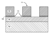
도 1b는 종래의 이종 본딩된 웨이퍼 구조체로부터 형성되는 종래의 핀(fin)들의 단면도를 예시한다.
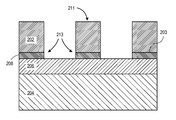
도 2a는 본 발명의 일 실시예에 따라, 캡슐화 층을 갖는 이종 본딩된 웨이퍼 구조체의 단면도를 예시한다.
도 2b는 본 발명의 일 실시예에 따라, 캡슐화 층을 갖는 이종 본딩된 웨이퍼 구조체로 형성되는 핀들의 단면도를 예시한다.
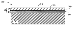
도 3a 내지 도 3d는 본 발명의 일 실시예에 따라, 제2 기판과의 본딩을 위해 제1 기판을 준비하는 방법의 단면도들을 예시한다.
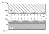
도 4a 내지 도 4c는 본 발명의 일 실시예에 따라, 제1 기판과의 본딩을 위해 제2 기판을 준비하는 방법의 단면도들을 예시한다.
도 5a 내지 도 5b는 본 발명의 일 실시예에 따라, 제1 기판과 제2 기판을 본딩하는 방법의 단면도들을 예시한다.
도 6a는 본 발명의 일 실시예에 따라, 산화물 층에 의해 기판에 이종 부착되는 캡슐화 층을 갖는 핀을 포함하는 비평면적 finFET 디바이스의 등각도를 예시한다.
도 6b는 본 발명의 일 실시예에 따라, 산화물 층에 의해 기판에 이종 부착되는 캡슐화 층을 갖는 핀을 포함하는 비평면적 finFET 디바이스의 단면도를 예시한다.
도 7은 본 발명의 하나 이상의 실시예들을 구현하는 인터포저(interposer)를 예시한다.
도 8은 본 발명의 일 실시예에 따라 구축되는 컴퓨팅 디바이스를 예시한다.
Claims (25)
- 기판들을 본딩(bonding)하는 방법으로서,
제1 반도체 기판을 제공하는 단계;
상기 제1 반도체 기판의 최상부 상에 캡슐화 층을 형성하는 단계 ― 상기 캡슐화 층은, 산화제에 노출될 때 안정한 산화물을 생성하는 캡슐화 재료로 형성됨 ―;
상기 캡슐화 층의 최상부 상에 제1 본딩 층을 형성하는 단계 ― 상기 제1 본딩 층은 제1 최상부 표면을 가짐 ―;
제2 반도체 기판을 제공하는 단계;
상기 제2 반도체 기판의 최상부 상에 제2 본딩 층을 형성하는 단계 ― 상기 제2 본딩 층은 제2 최상부 표면을 가짐 ―; 및
상기 제1 최상부 표면을 상기 제2 최상부 표면에 본딩함으로써 상기 제1 반도체 기판을 상기 제2 반도체 기판에 부착하는 단계를 포함하는,
기판들을 본딩하는 방법. - 제1항에 있어서,
상기 제1 반도체 기판은, 산화제에 노출될 때 불안정한 산화물을 생성하는 제1 반도체 재료를 포함하는,
기판들을 본딩하는 방법. - 제2항에 있어서,
상기 제1 반도체 재료는 게르마늄을 포함하는,
기판들을 본딩하는 방법. - 제2항에 있어서,
상기 산화제는 산소 및 물 중 적어도 하나인,
기판들을 본딩하는 방법. - 제1항에 있어서,
상기 캡슐화 재료는 실리콘을 포함하는,
기판들을 본딩하는 방법. - 제1항에 있어서,
상기 제1 최상부 표면 및 상기 제2 최상부 표면을 표면 처리하는 단계를 더 포함하는,
기판들을 본딩하는 방법. - 제6항에 있어서,
상기 제1 최상부 표면 및 상기 제2 최상부 표면을 표면 처리하는 단계는, 상기 제1 최상부 표면 및 상기 제2 최상부 표면에 하이드록시 말단(hydroxyl termination)을 생성하는,
기판들을 본딩하는 방법. - 제1항에 있어서,
상기 제1 반도체 기판을 상기 제2 반도체 기판에 부착하는 단계는, 상기 제1 본딩 층 및 상기 제2 본딩 층의 확산 본딩에 의해 수행되는,
기판들을 본딩하는 방법. - 제8항에 있어서,
열적 어닐링을 적용하는 단계를 더 포함하는,
기판들을 본딩하는 방법. - 제1항에 있어서,
상기 제1 본딩 층 및 상기 제2 본딩 층을 형성하는 단계는 퇴적 프로세스에 의해 형성되는,
기판들을 본딩하는 방법. - 제10항에 있어서,
상기 퇴적 프로세스는, 실리콘 산화물 재료를 퇴적하는 CVD 프로세스인,
기판들을 본딩하는 방법. - 제1항에 있어서,
상기 제1 본딩 층을 형성하는 단계는 산화에 의해 수행되는,
기판들을 본딩하는 방법. - 본딩된 반도체 구조체로서,
제1 반도체 기판;
제2 반도체 기판;
상기 제1 반도체 기판과 상기 제2 반도체 기판 사이에 배치되는 본딩 층 ― 상기 본딩 층은 상기 제1 반도체 기판을 상기 제2 반도체 기판에 부착시킴 ―; 및
상기 제1 반도체 기판과 상기 본딩 층 사이에 배치되는 캡슐화 층을 포함하는,
본딩된 반도체 구조체. - 제13항에 있어서,
상기 제1 반도체 기판은 게르마늄을 포함하는,
본딩된 반도체 구조체. - 제13항에 있어서,
상기 제2 반도체 기판은 실리콘을 포함하는,
본딩된 반도체 구조체. - 제13항에 있어서,
상기 캡슐화 층은 실리콘을 포함하는,
본딩된 반도체 구조체. - 제13항에 있어서,
상기 캡슐화 층은 2 내지 6 nm 범위의 두께를 갖는,
본딩된 반도체 구조체. - 제13항에 있어서,
상기 본딩 층은, 2 내지 3 J/m2의 접착 강도로 상기 제1 기판을 상기 제2 기판에 본딩하는,
본딩된 반도체 구조체. - 제13항에 있어서,
상기 본딩 층은 50 내지 150 nm 범위의 두께를 갖는,
본딩된 반도체 구조체. - 컴퓨터 디바이스로서,
마더보드;
상기 마더보드 상에 장착되는 프로세서; 및
상기 프로세서와 동일한 칩 상에 제조되거나 상기 마더보드 상에 장착되는 통신 칩을 포함하고,
상기 프로세서는,
제1 반도체 기판;
제2 반도체 기판;
상기 제1 반도체 기판과 상기 제2 반도체 기판 사이에 배치되는 본딩 층 ― 상기 본딩 층은 상기 제1 반도체 기판을 상기 제2 반도체 기판에 부착시킴 ―; 및
상기 제1 반도체 기판과 상기 본딩 층 사이에 배치되는 캡슐화 층을 포함하는,
컴퓨터 디바이스. - 제20항에 있어서,
상기 제1 반도체 기판은 게르마늄을 포함하는,
컴퓨터 디바이스. - 제20항에 있어서,
상기 제2 반도체 기판은 실리콘을 포함하는,
컴퓨터 디바이스. - 제20항에 있어서,
상기 캡슐화 층은 실리콘을 포함하는,
컴퓨터 디바이스. - 제23항에 있어서,
상기 캡슐화 층은 에피택셜(epitaxial) 실리콘인,
컴퓨터 디바이스. - 제20항에 있어서,
상기 캡슐화 층은 2 내지 6 nm 범위의 두께를 갖는,
컴퓨터 디바이스.
Applications Claiming Priority (1)
| Application Number | Priority Date | Filing Date | Title |
|---|---|---|---|
| PCT/US2014/042316 WO2015191082A1 (en) | 2014-06-13 | 2014-06-13 | Surface encapsulation for wafer bonding |
Publications (2)
| Publication Number | Publication Date |
|---|---|
| KR20170017880A true KR20170017880A (ko) | 2017-02-15 |
| KR102206378B1 KR102206378B1 (ko) | 2021-01-22 |
Family
ID=54834029
Family Applications (1)
| Application Number | Title | Priority Date | Filing Date |
|---|---|---|---|
| KR1020167031258A Active KR102206378B1 (ko) | 2014-06-13 | 2014-06-13 | 웨이퍼 본딩을 위한 표면 캡슐화 |
Country Status (7)
| Country | Link |
|---|---|
| US (1) | US20170062569A1 (ko) |
| EP (1) | EP3155656A4 (ko) |
| JP (1) | JP6428788B2 (ko) |
| KR (1) | KR102206378B1 (ko) |
| CN (1) | CN106463416A (ko) |
| TW (1) | TWI616927B (ko) |
| WO (1) | WO2015191082A1 (ko) |
Families Citing this family (9)
| Publication number | Priority date | Publication date | Assignee | Title |
|---|---|---|---|---|
| US8735219B2 (en) | 2012-08-30 | 2014-05-27 | Ziptronix, Inc. | Heterogeneous annealing method and device |
| WO2017165146A1 (en) | 2016-03-23 | 2017-09-28 | Invensense, Inc. | Integration of ain ultrasonic transducer on a cmos substrate using fusion bonding process |
| CN108122823B (zh) * | 2016-11-30 | 2020-11-03 | 中芯国际集成电路制造(上海)有限公司 | 晶圆键合方法及晶圆键合结构 |
| CN112368828A (zh) * | 2018-07-03 | 2021-02-12 | 伊文萨思粘合技术公司 | 在微电子学中用于接合异种材料的技术 |
| WO2020010056A1 (en) | 2018-07-03 | 2020-01-09 | Invensas Bonding Technologies, Inc. | Techniques for joining dissimilar materials in microelectronics |
| JP7205273B2 (ja) * | 2019-02-12 | 2023-01-17 | 富士通株式会社 | 電子装置及び認証装置 |
| WO2021188846A1 (en) | 2020-03-19 | 2021-09-23 | Invensas Bonding Technologies, Inc. | Dimension compensation control for directly bonded structures |
| CN115101494B (zh) * | 2022-06-02 | 2025-11-07 | 芯盟科技有限公司 | 键合用结构及其制备方法、以及半导体装置 |
| CN115410920B (zh) * | 2022-09-23 | 2026-05-12 | 广东省大湾区集成电路与系统应用研究院 | 半导体器件的制作方法以及半导体器件 |
Citations (8)
| Publication number | Priority date | Publication date | Assignee | Title |
|---|---|---|---|---|
| US6410371B1 (en) * | 2001-02-26 | 2002-06-25 | Advanced Micro Devices, Inc. | Method of fabrication of semiconductor-on-insulator (SOI) wafer having a Si/SiGe/Si active layer |
| JP2005302967A (ja) * | 2004-04-09 | 2005-10-27 | Sumco Corp | Soiウェーハの製造方法 |
| JP2007511068A (ja) * | 2003-11-03 | 2007-04-26 | インターナショナル・ビジネス・マシーンズ・コーポレーション | 絶縁体上SiGe(SGOI)基板及び絶縁体上Ge(GOI)基板の製造方法、半導体ウェハ、並びに半導体構造 |
| JP2007201430A (ja) * | 2006-01-23 | 2007-08-09 | Soi Tec Silicon On Insulator Technologies Sa | 電気特性を向上させた複合基板の作製方法 |
| JP2011502358A (ja) * | 2007-10-31 | 2011-01-20 | コーニング インコーポレイテッド | 半導体・オン・インシュレータ装置を形成するための基板組成および方法の改善 |
| US20110039395A1 (en) * | 2008-06-25 | 2011-02-17 | Semiconductor Energy Laboratory Co., Ltd. | Method for manufacturing soi substrate |
| JP2013110161A (ja) * | 2011-11-17 | 2013-06-06 | National Institute Of Advanced Industrial & Technology | 素子形成用基板及びその製造方法 |
| JP2014508396A (ja) * | 2010-12-21 | 2014-04-03 | インテル コーポレイション | トランジスタ装置、集積回路及び製造方法 |
Family Cites Families (12)
| Publication number | Priority date | Publication date | Assignee | Title |
|---|---|---|---|---|
| US8994104B2 (en) * | 1999-09-28 | 2015-03-31 | Intel Corporation | Contact resistance reduction employing germanium overlayer pre-contact metalization |
| US6500694B1 (en) * | 2000-03-22 | 2002-12-31 | Ziptronix, Inc. | Three dimensional device integration method and integrated device |
| US7148526B1 (en) * | 2003-01-23 | 2006-12-12 | Advanced Micro Devices, Inc. | Germanium MOSFET devices and methods for making same |
| FR2891281B1 (fr) * | 2005-09-28 | 2007-12-28 | Commissariat Energie Atomique | Procede de fabrication d'un element en couches minces. |
| US7781308B2 (en) * | 2007-12-03 | 2010-08-24 | Semiconductor Energy Laboratory Co., Ltd. | Method for manufacturing SOI substrate |
| US20090186190A1 (en) * | 2008-01-17 | 2009-07-23 | Shan Guan | Silicon filter |
| JP5355504B2 (ja) * | 2009-07-30 | 2013-11-27 | 株式会社東芝 | 半導体装置の製造方法および半導体装置 |
| US9608119B2 (en) * | 2010-03-02 | 2017-03-28 | Micron Technology, Inc. | Semiconductor-metal-on-insulator structures, methods of forming such structures, and semiconductor devices including such structures |
| KR101144840B1 (ko) * | 2010-06-08 | 2012-05-14 | 삼성코닝정밀소재 주식회사 | 접합기판 제조방법 |
| US8502279B2 (en) * | 2011-05-16 | 2013-08-06 | Globalfoundries Singapore Pte. Ltd. | Nano-electro-mechanical system (NEMS) structures with actuatable semiconductor fin on bulk substrates |
| DE102011089569B4 (de) * | 2011-12-22 | 2024-08-22 | Robert Bosch Gmbh | Verfahren zum Verbinden zweier Siliziumsubstrate und entsprechende Anordnung zweier Siliziumsubstrate |
| US9362277B2 (en) * | 2014-02-07 | 2016-06-07 | Globalfounries Inc. | FinFET with multilayer fins for multi-value logic (MVL) applications and method of forming |
-
2014
- 2014-06-13 CN CN201480078790.3A patent/CN106463416A/zh active Pending
- 2014-06-13 US US15/119,119 patent/US20170062569A1/en not_active Abandoned
- 2014-06-13 WO PCT/US2014/042316 patent/WO2015191082A1/en not_active Ceased
- 2014-06-13 JP JP2016565670A patent/JP6428788B2/ja not_active Expired - Fee Related
- 2014-06-13 KR KR1020167031258A patent/KR102206378B1/ko active Active
- 2014-06-13 EP EP14894732.8A patent/EP3155656A4/en not_active Withdrawn
-
2015
- 2015-05-04 TW TW104114140A patent/TWI616927B/zh not_active IP Right Cessation
Patent Citations (8)
| Publication number | Priority date | Publication date | Assignee | Title |
|---|---|---|---|---|
| US6410371B1 (en) * | 2001-02-26 | 2002-06-25 | Advanced Micro Devices, Inc. | Method of fabrication of semiconductor-on-insulator (SOI) wafer having a Si/SiGe/Si active layer |
| JP2007511068A (ja) * | 2003-11-03 | 2007-04-26 | インターナショナル・ビジネス・マシーンズ・コーポレーション | 絶縁体上SiGe(SGOI)基板及び絶縁体上Ge(GOI)基板の製造方法、半導体ウェハ、並びに半導体構造 |
| JP2005302967A (ja) * | 2004-04-09 | 2005-10-27 | Sumco Corp | Soiウェーハの製造方法 |
| JP2007201430A (ja) * | 2006-01-23 | 2007-08-09 | Soi Tec Silicon On Insulator Technologies Sa | 電気特性を向上させた複合基板の作製方法 |
| JP2011502358A (ja) * | 2007-10-31 | 2011-01-20 | コーニング インコーポレイテッド | 半導体・オン・インシュレータ装置を形成するための基板組成および方法の改善 |
| US20110039395A1 (en) * | 2008-06-25 | 2011-02-17 | Semiconductor Energy Laboratory Co., Ltd. | Method for manufacturing soi substrate |
| JP2014508396A (ja) * | 2010-12-21 | 2014-04-03 | インテル コーポレイション | トランジスタ装置、集積回路及び製造方法 |
| JP2013110161A (ja) * | 2011-11-17 | 2013-06-06 | National Institute Of Advanced Industrial & Technology | 素子形成用基板及びその製造方法 |
Also Published As
| Publication number | Publication date |
|---|---|
| EP3155656A1 (en) | 2017-04-19 |
| EP3155656A4 (en) | 2018-02-14 |
| TW201606849A (zh) | 2016-02-16 |
| WO2015191082A1 (en) | 2015-12-17 |
| KR102206378B1 (ko) | 2021-01-22 |
| CN106463416A (zh) | 2017-02-22 |
| JP6428788B2 (ja) | 2018-11-28 |
| JP2017523588A (ja) | 2017-08-17 |
| US20170062569A1 (en) | 2017-03-02 |
| TWI616927B (zh) | 2018-03-01 |
Similar Documents
| Publication | Publication Date | Title |
|---|---|---|
| KR102206378B1 (ko) | 웨이퍼 본딩을 위한 표면 캡슐화 | |
| KR102309334B1 (ko) | 반도체 디바이스들을 위해 희생 차단 층들을 이용하는 선택적 퇴적 | |
| KR102375846B1 (ko) | 게이트-올-어라운드 트랜지스터들을 위한 gaas 상의 부정형 ingaas | |
| US9754778B2 (en) | Metallization of fluorocarbon-based dielectric for interconnects | |
| US20200144369A1 (en) | Integrated circuit components with substrate cavities | |
| US11538803B2 (en) | Integration of III-V transistors in a silicon CMOS stack | |
| US10861870B2 (en) | Inverted staircase contact for density improvement to 3D stacked devices | |
| KR102309367B1 (ko) | 비대칭 프로파일을 갖는 핀 구조체들을 형성하는 방법 및 장치 | |
| US11710765B2 (en) | High aspect ratio non-planar capacitors formed via cavity fill | |
| KR102351550B1 (ko) | 측벽 라이너를 갖는 핀 구조를 형성하는 장치 및 방법 | |
| CN107210194A (zh) | 包括隧穿层的晶体管的制作 | |
| JP2017522714A (ja) | 層転写による分極反転基板上の高電子移動度トランジスタ製造処理 | |
| KR20210142526A (ko) | 인 도펀트 농도가 높은 소스 또는 드레인 구조물 | |
| US20230395467A1 (en) | Glass core architectures with dielectric buffer layer between glass core and metal vias and pads | |
| US20220416017A1 (en) | Buried power rail with a silicide layer for well biasing | |
| TW201737489A (zh) | 用於電壓調節的矽p型金屬氧化物半導體(pmos)與氮化鎵n型金屬氧化物半導體(nmos) | |
| US20230395445A1 (en) | Glass core architectures with dielectric buffer layer between glass core and metal vias and pads | |
| CN110634940A (zh) | 使用横向外延过生长制造肖特基势垒二极管 | |
| US20240290835A1 (en) | Nanoribbon-based transistors with etch stop layer to assist subfin removal | |
| US20240222435A1 (en) | Coupling a layer of silicon carbide with an adjacent layer | |
| US20240304621A1 (en) | Fabrication of nanoribbon-based transistors using patterned foundation | |
| US20250098239A1 (en) | Air gap insulation in place of gate spacers | |
| EP4425540A1 (en) | Metal gate fabrication for nanoribbon-based transistors | |
| US20240224504A1 (en) | Dynamic random-access memory using wide band gap materials | |
| US20240222228A1 (en) | Devices in a silicon carbide layer coupled with devices in a gallium nitride layer |
Legal Events
| Date | Code | Title | Description |
|---|---|---|---|
| PA0105 | International application |
St.27 status event code: A-0-1-A10-A15-nap-PA0105 |
|
| PG1501 | Laying open of application |
St.27 status event code: A-1-1-Q10-Q12-nap-PG1501 |
|
| A201 | Request for examination | ||
| PA0201 | Request for examination |
St.27 status event code: A-1-2-D10-D11-exm-PA0201 |
|
| E902 | Notification of reason for refusal | ||
| PE0902 | Notice of grounds for rejection |
St.27 status event code: A-1-2-D10-D21-exm-PE0902 |
|
| E13-X000 | Pre-grant limitation requested |
St.27 status event code: A-2-3-E10-E13-lim-X000 |
|
| P11-X000 | Amendment of application requested |
St.27 status event code: A-2-2-P10-P11-nap-X000 |
|
| P13-X000 | Application amended |
St.27 status event code: A-2-2-P10-P13-nap-X000 |
|
| E701 | Decision to grant or registration of patent right | ||
| PE0701 | Decision of registration |
St.27 status event code: A-1-2-D10-D22-exm-PE0701 |
|
| GRNT | Written decision to grant | ||
| PR0701 | Registration of establishment |
St.27 status event code: A-2-4-F10-F11-exm-PR0701 |
|
| PR1002 | Payment of registration fee |
St.27 status event code: A-2-2-U10-U12-oth-PR1002 Fee payment year number: 1 |
|
| PG1601 | Publication of registration |
St.27 status event code: A-4-4-Q10-Q13-nap-PG1601 |
|
| PR1001 | Payment of annual fee |
St.27 status event code: A-4-4-U10-U11-oth-PR1001 Fee payment year number: 4 |
|
| P22-X000 | Classification modified |
St.27 status event code: A-4-4-P10-P22-nap-X000 |
|
| PR1001 | Payment of annual fee |
St.27 status event code: A-4-4-U10-U11-oth-PR1001 Fee payment year number: 5 |
|
| PR1001 | Payment of annual fee |
St.27 status event code: A-4-4-U10-U11-oth-PR1001 Fee payment year number: 6 |
|
| U11 | Full renewal or maintenance fee paid |
Free format text: ST27 STATUS EVENT CODE: A-4-4-U10-U11-OTH-PR1001 (AS PROVIDED BY THE NATIONAL OFFICE) Year of fee payment: 6 |
|
| P22-X000 | Classification modified |
St.27 status event code: A-4-4-P10-P22-nap-X000 |