KR20170032017A - Multilayered inductor - Google Patents
Multilayered inductor Download PDFInfo
- Publication number
- KR20170032017A KR20170032017A KR1020150129742A KR20150129742A KR20170032017A KR 20170032017 A KR20170032017 A KR 20170032017A KR 1020150129742 A KR1020150129742 A KR 1020150129742A KR 20150129742 A KR20150129742 A KR 20150129742A KR 20170032017 A KR20170032017 A KR 20170032017A
- Authority
- KR
- South Korea
- Prior art keywords
- cover portion
- coil
- disposed
- inductance
- magnetic
- Prior art date
- Legal status (The legal status is an assumption and is not a legal conclusion. Google has not performed a legal analysis and makes no representation as to the accuracy of the status listed.)
- Ceased
Links
Images


Classifications
-
- H—ELECTRICITY
- H01—ELECTRIC ELEMENTS
- H01F—MAGNETS; INDUCTANCES; TRANSFORMERS; SELECTION OF MATERIALS FOR THEIR MAGNETIC PROPERTIES
- H01F17/00—Fixed inductances of the signal type
- H01F17/0006—Printed inductances
- H01F17/0013—Printed inductances with stacked layers
-
- H—ELECTRICITY
- H01—ELECTRIC ELEMENTS
- H01F—MAGNETS; INDUCTANCES; TRANSFORMERS; SELECTION OF MATERIALS FOR THEIR MAGNETIC PROPERTIES
- H01F17/00—Fixed inductances of the signal type
- H01F17/02—Fixed inductances of the signal type without magnetic core
-
- H—ELECTRICITY
- H01—ELECTRIC ELEMENTS
- H01F—MAGNETS; INDUCTANCES; TRANSFORMERS; SELECTION OF MATERIALS FOR THEIR MAGNETIC PROPERTIES
- H01F27/00—Details of transformers or inductances, in general
- H01F27/28—Coils; Windings; Conductive connections
- H01F27/2804—Printed windings
Landscapes
- Engineering & Computer Science (AREA)
- Power Engineering (AREA)
- Microelectronics & Electronic Packaging (AREA)
- Coils Or Transformers For Communication (AREA)
Abstract
Description
본 개시는 적층 인덕터에 관한 것이다.
The present disclosure relates to a stacked inductor.
일반적인 적층 인덕터는 도체패턴이 형성된 복수의 자성체 층을 적층한 구조를 가지며, 상기 도체패턴은 각 자성체 층에 형성된 도전성 비아에 의해 순차적으로 접속되어 적층방향에 따라 중첩되면서 나선구조를 갖는 코일을 이룬다. 또한, 상기 코일의 양단은 적층체의 외부면에 인출되어 외부단자와 접속된 구조를 갖는다.
A typical laminated inductor has a structure in which a plurality of magnetic material layers on which conductor patterns are formed are laminated. The conductor patterns are sequentially connected by conductive vias formed in the respective magnetic material layers, and are superimposed along the lamination direction to form a coil having a spiral structure. Both ends of the coil are drawn to the outer surface of the laminate and connected to the external terminals.
이와 같이, 적층 인덕터는 코일이 자성체로 둘러싸여 있으므로, 자기 누설이 게 발생하게 되며, 적층 칩 구조를 가지므로 소형화와 박형화에 유리한 장점을 가진다.
As described above, in the multilayer inductor, since the coil is surrounded by the magnetic body, magnetic leakage occurs, and since the multilayer inductor has the multilayer chip structure, it is advantageous in downsizing and thinning.
하지만, 이러한 장점에도 불구하고, 적층 인덕터는 DC 바이어스(bias) 특성을 확보할 수 있으나, 자성체의 자기포화에 의하여 급격한 인덕턴스(inductance) 저하(DC 중첩 특성 저하)가 발생하는 단점이 있다. 따라서, 이러한 급격한 인덕턴스 저하를 방지하고자 하는 연구가 이루어지고 있다.
However, in spite of this advantage, the stacked inductor can secure the DC bias characteristic, but has a disadvantage in that a sudden inductance deterioration (DC superposition characteristic deterioration) occurs due to magnetic saturation of the magnetic body. Therefore, studies have been made to prevent such a sudden drop in inductance.
종래에는 도체패턴이 형성되는 일부 층을 전기적 절연성을 갖는 비자성체층으로 대체하거나, 도체패턴이 형성되는 일부 층에서 일부영역을 전기적 절연성을 갖는 비자성체 물질로 형성하는 방법을 제안하고 있다.
There has been proposed a method of replacing some layers in which a conductor pattern is formed with a nonmagnetic layer having electrical insulation or forming a portion of a certain layer in which a conductor pattern is formed from a nonmagnetic material having electrical insulation properties.
하지만, 이러한 방안에 따르면, 이종인 비자성체 재료의 선택으로 사용되는 재료가 증가할 수 있으며, 그에 따른 별도의 공정이 요구되는 공정상 번거로움이 있다.
However, according to this method, there is an increase in the materials used as the selection of heterogeneous nonmagnetic materials, and there is a processing hassle in which a separate process is required.
특히, 도체패턴이 형성되는 일부 층에서 일부 영역을 대체할 경우에는 시트 제조공정이 상당히 복잡해지는 문제가 있으며, 인덕턴스 특성을 조정하는 것에 어려움이 있다.
Particularly, in the case where a certain region is substituted for a certain layer in which a conductor pattern is formed, there is a problem that the sheet manufacturing process becomes considerably complicated, and it is difficult to adjust the inductance characteristic.
따라서, 인덕턴스 특성 및 DC 바이어스 특성을 모두 확보할 수 있는 적층 인덕터를 얻는 것이 매우 중요한 실정이다.
Therefore, it is very important to obtain a laminated inductor capable of ensuring both inductance characteristics and DC bias characteristics.
한편, 비자성체층을 도체 패턴이 형성되는 일부 층에 대체할 경우 인덕턴스 특성을 조정하는 것에 어려움이 있다.
On the other hand, when the non-magnetic layer is replaced with a layer in which the conductor pattern is formed, it is difficult to adjust the inductance characteristics.
본 개시의 여러 목적 중 하나는 인덕턴스 특성을 향상시키면서, DC 바이어스 특성을 개선할 수 있는 적층 인덕터를 제공하는 것이다.
One of the objects of the present disclosure is to provide a laminated inductor capable of improving DC bias characteristics while improving inductance characteristics.
본 개시를 통하여 제안하는 여러 해결 수단 중 하는 적층 인덕터의 커버부의 내부 영역 중 커버부의 표면으로부터 이격된 일 영역에 배치된 비자성체를 포함하여, 인덕턴스 특성을 향상시킴과 동시에 DC 바이어스 특성을 개선할 수 있도록 하는 것이다.
It is possible to improve the inductance characteristic and to improve the DC bias characteristic by including the nonmagnetic material disposed in one region of the inner region of the cover portion of the laminated inductor among the various solutions proposed through the present disclosure and spaced from the surface of the cover portion .
본 개시의 일 실시 예에 따른 적층 인덕터는 인덕턴스 특성을 향상시키면서, DC 바이어스 특성을 개선할 수 있다.
The stacked inductor according to one embodiment of the present disclosure can improve the DC bias characteristic while improving the inductance characteristic.
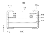
도 1은 본 개시의 일 실시 예에 따른 적층 인덕터의 사시도를 개략적으로 도시한 것이다.
도 2는 본 개시의 일 실시 예에 따른 적층 인덕터의 단면도를 개략적으로 도시한 것이다,.
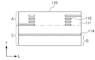
도 3은 본 개시의 일 실시 예에 따른 적층 인덕터의 본체의 단면도를 개략적으로 도시한 것이다.
도 4는 본 개시의 일 실시 예에 따른 적층 인덕터의 비자성체층 위치에 따른 인덕턴스의 변화 거동을 나타낸 그래프를 도시한 것이다.Figure 1 schematically illustrates a perspective view of a stacked inductor in accordance with one embodiment of the present disclosure;
Figure 2 schematically illustrates a cross-sectional view of a stacked inductor in accordance with one embodiment of the present disclosure;
Figure 3 schematically illustrates a cross-sectional view of a body of a stacked inductor in accordance with one embodiment of the present disclosure;
4 is a graph showing a variation behavior of inductance according to a position of a non-magnetic layer of a laminated inductor according to an embodiment of the present disclosure.
이하, 첨부된 도면을 참조하여 본 개시에 대해 보다 상세히 설명한다. 도면에서 요소들의 형상 및 크기 등은 보다 명확한 설명을 위해 과장될 수 있다.
Hereinafter, the present disclosure will be described in more detail with reference to the accompanying drawings. The shape and size of elements in the drawings may be exaggerated for clarity.
이하, 본 개시에 의한 코일 부품에 대하여 설명한다.
Hereinafter, the coil component according to the present disclosure will be described.
도 1은 본 개시의 일 실시 예에 따른 적층 인덕터의 사시도를 개략적으로 도시한 것이고, 도 2는 본 개시의 일 실시 예에 따른 적층 인덕터의 단면도를 개략적으로 도시한 것이며, 도 3은 본 개시의 일 실시 예에 따른 적층 인덕터의 본체의 단면도를 개략적으로 도시한 것이다.Figure 1 schematically illustrates a perspective view of a stacked inductor in accordance with one embodiment of the present disclosure, Figure 2 schematically illustrates a cross-sectional view of a stacked inductor in accordance with one embodiment of the present disclosure, Sectional view of a body of a stacked inductor according to one embodiment.
도 1 내지 도 3을 참조하면, 본 개시의 일 실시 예에 따른 적층 인덕터(100)는 코일부(A), 상기 코일부(A) 상부 및 하부 중 적어도 하나에 배치된 커버부(C) 및 상기 커버부(C)의 내부 영역 중 상기 커버부(C)의 표면과 이격된 일 영역에 배치된 비자성체층(114)을 포함한다.
1 to 3, a laminated
구체적으로, 본 개시의 적층 인덕터(100)는 복수의 자성체 층(111)이 적층된 구조를 구비하며, 코일부(A) 및 상기 코일부(A)의 상부 및 하부 중 적어도 하나에 배치된 커버부(C)를 포함하는 본체(110);를 포함하며, 상기 커버부(C)는 상기 커버부(C)의 내부 영역 중 표면과 이격된 일 영역에 배치된 비자성체층(114)을 포함한다.
Specifically, the laminated
상기 본체(110)는 페라이트를 포함하는 복수의 자성체 층(111)을 두께 방향으로 적층하여 형성될 수 있다.The
상기 자성체 층(111)은 소성 후에 경계를 거의 확인할 수 없을 만큼 일체화될 수 있다. 이러한 본체(110)의 형상, 치수 및 자성체 층의 적층 수가 본 개시의 실시 예에 도시된 것으로 한정되는 것은 아니다.
The
상기 본체(110)는 코일부(A) 및 커버부(C)을 포함한다.The
상기 코일부(C)는 상기 자성체 층(111) 상에 코일(112)을 형성하여 형성될 수 있다.The coil portion C may be formed by forming a
상기 코일(112)은 전기 전도성이 우수한 재료를 사용하여 형성할 수 있으며, 예를 들어 은(Ag) 또는 구리(Cu)와 같은 도전성 재료 또는 이들의 합금을 포함하여 형성할 수 있으나, 본 개시는 이에 한정되는 것은 아니다.The
상기 코일(112)은 인접하는 상부 및 하부의 코일(112)과 도전성 비아(미도시)를 통해 전기적으로 연결될 수 있다.
The
상기 커버부(C)는 상기 코일부(A)의 상부 및 하부 중 적어도 하나에 배치된다. 상기 커버부(C)는 상기 코일부(A)의 하부에 배치될 수 있으나, 이에 한정되는 것은 아니다.The cover portion (C) is disposed on at least one of the upper portion and the lower portion of the coil portion (A). The cover portion C may be disposed under the coil portion A, but is not limited thereto.
상기 커버부(C)는 상기 자성체 층과 동일한 재료로 이루어진 페이스트를 일정 두께로 인쇄하여 형성될 수 있다.
The cover portion C may be formed by printing a paste made of the same material as the magnetic material layer to a predetermined thickness.
도 1을 참조하면, 상기 본체(110)의 양 단면에 외부전극(115a, 115b)이 배치된다.Referring to FIG. 1,
상기 외부전극(115a, 115b)은 전기 전도성이 우수한 재료를 사용하여 형성될 수 있으며, 예를 들어 은(Ag) 또는 구리(Cu)와 같은 도전성 재료 또는 이들의 합금을 포함하여 형성될 수 있으나, 본 개시가 이에 한정되는 것은 아니다.The
또한, 이렇게 형성된 외부전극(115a, 115b)의 표면에 필요 시 니켈(Ni) 또는 주성(Sn)을 도금 처리하여 도금층이 더 형성될 수 있다.
The surface of the
상기와 같은 구성을 가지는 인덕터에서는 코일이 외부전극과 전기적으로 연결되면 코일을 중심으로 자기장이 형성되는데, 층층이 형성되어 있는 코일에서 발생하는 자기장이 중첩되어 자기장이 형성된다.In the inductor having the above-described configuration, when the coil is electrically connected to the external electrode, a magnetic field is formed around the coil, and the magnetic field generated from the coil in which the layer is formed overlaps to form a magnetic field.
이와 같이 형성된 자기장의 자속은 상기 코일의 중심을 따라 흐르게 된다. 이러한 자기장은 자성체의 자기 포화에 의하여 급격한 인덕턴스 저하가 발생할 수 있다.The magnetic flux of the magnetic field thus formed flows along the center of the coil. Such a magnetic field may cause a sharp inductance drop due to magnetic saturation of the magnetic body.
따라서, 이러한 급격한 인덕턴스 저하를 방지하기 위하여, 상기 비자성체층(114)을 상기 커버부(C)의 내부 영역에 배치할 수 있다.Therefore, in order to prevent such rapid inductance degradation, the
상기 비자성체층(114)이 자기 포화를 지연시킬 수 있으므로, 자기 포화로 인한 인덕턴스 저하를 개선할 수 있다.The
즉, 비자성체층(114)에 의하여 적층형 전자부품(100)의 인덕턴스 특성이 변화할 수 있다.
That is, the inductance characteristics of the multilayer
종래에는 비자성체층을 코일부의 내부 영역에 배치하여 적층 인덕터의 인덕턴스 특성을 구현하였다. Conventionally, inductance characteristics of a laminated inductor are realized by disposing a nonmagnetic layer in an inner region of a coil portion.
인덕터에서 코일부 내부의 비자성체층의 역할이 작을수록 인덕턴스 특성이 높아질 수 있는데, 인덕턴스 특성을 구현하는 범위를 증가시키는 방안으로 코일부 내부에 비자성체를 배치하는 것은 한계가 있다.
The smaller the role of the nonmagnetic layer in the coil part of the inductor, the higher the inductance characteristics can be. However, placing the nonmagnetic part in the coil part is limited in order to increase the range of realizing the inductance characteristic.
인덕턴스 특성은 상기 비자성체의 위치에 따라 구현 범위가 달라질 수 있다.The inductance characteristic may vary depending on the position of the non-magnetic body.
도 3을 참조하면, 본 개시의 일 실시 예에 따른 비자성체층(114)은 상기 커버부(C)의 표면과 상기 커버부(C)의 두께의 25%이상의 거리로 이격된 일 영역에 배치됨과 동시에, 상기 코일부(A)와 인접한 영역에 배치되어, 적층 인덕터의 인덕턴스 특성을 향상시킬 수 있으며, 이와 동시에 DC 바이어스 특성을 개선할 수 있다.3, the
상기 커버부(C)의 표면과 상기 커버부(C)의 표면으로부터 상기 커버부의 두께(C)의 25%의 거리로 이격된 영역 사이를 갭(gap) 영역(G)이라고 할 때, 상기 비자성체층(114)은 상기 커버부(C)의 내부 영역 중 상기 갭 영역(G)을 제외한 영역에 배치될 수 있다.When a gap region G is defined as a gap between a surface of the cover portion C and a surface of the cover portion C spaced by a distance of 25% of the thickness C of the cover portion, The
상기 비자성체층(114)은 상기 코일부(A)와 접하여 형성될 수 있으나, 이에 한정되는 것은 아니다.The
예를 들면, 상기 커버부(C)의 두께가 200μm인 경우, 상기 비자성체층(114)은 상기 커버부(C)의 표면으로부터 50μm 이상 이격된 영역에 배치될 수 있다. For example, when the thickness of the cover portion C is 200 占 퐉, the
상기 비자성체층(114)이 상기 코일부(A)의 외부에 배치되되, 상기 커버부(C)의 표면으로부터 이격된 영역에 배치되면, 인덕턴스 특성을 향상시킬 수 있으며, 이로 인해, DC 바이어스 특성 또한 개선될 수 있다.When the
상기 비자성체층(114)은 상기 커버부(C)의 표면과 상기 커버부(C)의 두께의 25% 내의 거리로 이격된 영역에 배치될 경우, 즉, 상기 비자성체층(114)이 갭 영역(G)의 내부에 배치될 경우, 저전류대 인덕턴스 변화 거동이 기존 적층 인덕터가 가질 수 있는 인덕턴스 거동과 달라질 수 있으므로, 자기 포화 저하 효과가 미비할 수 있다.
When the
상기 비자성체층(114)은 상기 본체(110)의 양 단면으로 노출될 수 있다.The
상기 비자성체층(114)은 상기 본체(110)의 양단면으로 노출되어 상기 외부전극과 접할 수 있다.
The
상기 커버부(C) 내부에 배치된 상기 비자성체층(114)은 상기 커버부(C)의 표면보다 코일부(A)에 더 인접하도록 배치될 수 있다.The
상기 비자성체층(114)은 상기 커버부(C)의 내부 영역에서 상기 코일부(A)에 더 인접할수록 인덕턴스 특성이 향상될 수 있다. 즉, 적층 인덕터의 구현 가능한 인덕턴스의 상한 범위를 향상시킬 수 있다.
The inductance characteristic can be improved as the
(실시예)(Example)
하기 표 1은 비자성체층이 커버부의 표면과 이격된 거리를 나타낸 표이며, 도 4는 본 개시의 일 실시 예에 따른 적층 인덕터의 비자성체층 위치에 따른 인덕턴스의 변화 거동을 나타낸 그래프를 도시한 것이다.
4 is a graph showing a variation behavior of inductance according to a position of a nonmagnetic layer of a laminated inductor according to an embodiment of the present disclosure; and FIG. 4 is a graph showing a change in inductance of the non- will be.
(μm)Thickness of cover part
(μm)
(μm)The distance between the non-magnetic layer and the surface of the cover portion
(μm)
(%)The thickness ratio of the cover portion to the distance between the non-magnetic layer and the surface of the cover portion
(%)
(μm)The distance between the surface in contact with the coil part and the nonmagnetic layer in the cover part
(μm)
*: 비교예
*: Comparative Example
본 개시의 비교예 및 실시예의 적층 인덕터의 커버부의 두께는 200μm이며, 상기 커버부의 표면과 상기 커버부의 두께의 12.5%, 25%, 37.5%, 50% 및 75%의 거리(25, 50, 75, 100, 150μm)로 이격된 영역에 비자성체를 배치하였다.The thicknesses of the cover portions of the laminated inductors of the comparative examples and the examples of this disclosure are 200 μm and the distances of 25.5, 50, and 75% of the thickness of the cover portion and the cover portion are 12.5%, 25%, 37.5% , 100, 150 mu m).
상기 비자성체를 포함하는 적층 인덕터에 전류를 인가하여 인덕턴스의 변화 거동을 측정하였다.
The change in inductance behavior was measured by applying current to the laminated inductor including the nonmagnetic body.
적층 인덕터에서 DC 바이어스 특성의 경우, 적층 인덕터에 전류 인가시 인덕턴스의 변화율의 영향을 받을 수 있다. 인덕턴스의 변화율 그래프를 봤을 때, 초기 전류값에서 변화율의 곡선이 완만한 형태를 유지하며, 특정 전류값에 도달하면 변화율의 곡선이 급격하게 변화하는 형태를 가질 수 있다.
In the case of the DC bias characteristic in the laminated inductor, the rate of change of the inductance when the current is applied to the laminated inductor can be influenced. When the graph of rate of change of inductance is taken into consideration, the curve of the rate of change is gentle at the initial current value, and the curve of the rate of change rapidly changes when a specific current value is reached.
도 4를 참조하면, 실시예 1 내지 4에서 비자성체층이 커버부의 표면과 이격된 거리가 클수록 인덕턴스의 변화율 그래프가 완만한 형상을 가지며, 특정 전류값이 높아짐을 알 수 있다.Referring to FIG. 4, it can be seen that, in Examples 1 to 4, as the distance between the non-magnetic layer and the surface of the cover increases, the curve of change in inductance has a gentle shape and a specific current value increases.
비교예 1, 즉 비자성체층이 커버부의 표면과 커버부의 두께의 12.5% 거리로 이격된 경우, 초기 전류값 인가시 인덕턴스 변화율 곡선이 급격하게 변화하는 것을 알 수 있다. 이 경우, DC 바이어스 특성이 낮아질 뿐만 아니라, 인덕턴스 특성을 확보할 수 없다. It can be seen that the curve of the inductance change rate abruptly changes when the initial current value is applied when the non-magnetic layer is separated by a distance of 12.5% of the thickness of the cover portion and the surface of the cover portion. In this case, not only the DC bias characteristic is lowered but also the inductance characteristic can not be secured.
따라서, 본 개시의 적층 인덕터는 커버부의 표면과 커버부의 두께의 25%이상 거리로 이격된 일 영역에 배치된 비자성체층을 포함함으로써, DC 바이어스 특성 및 인덕턴스 특성을 확보할 수 있다.
Therefore, the laminated inductor of the present disclosure includes a nonmagnetic layer disposed in a region separated by a distance of 25% or more of the thickness of the cover portion and the cover portion, thereby securing the DC bias characteristic and the inductance characteristic.
본 개시는 상술한 실시형태 및 첨부된 도면에 의해 한정되는 것이 아니며 첨부된 청구범위에 의해 한정하고자 한다.The present disclosure is not limited by the above-described embodiment and the accompanying drawings, but is intended to be limited by the appended claims.
따라서, 청구범위에 기재된 본 개시의 기술적 사상을 벗어나지 않는 범위 내에서 당 기술분야의 통상의 지식을 가진 자에 의해 다양한 형태의 치환, 변형 및 변경이 가능할 것이며, 이 또한 본 개시의 범위에 속한다고 할 것이다.
Accordingly, various modifications, substitutions, and alterations can be made by those skilled in the art without departing from the spirit of the present disclosure, which is also within the scope of the present disclosure something to do.
100: 적층 인덕터
110: 본체
111: 자성체 층
112: 코일
114: 비자성체층
115a, 115b: 제1 및 제2 외부 전극
C: 커버부
A: 코일부
G: 갭(gap) 영역100: laminated inductor
110:
111: magnetic layer
112: coil
114: nonmagnetic layer
115a, 115b: first and second external electrodes
C: Cover part
A: coil part
G: gap area
Claims (10)
상기 코일부의 상부 및 하부 중 적어도 하나에 배치된 커버부; 및
상기 커버부의 내부 영역 중 상기 커버부의 표면과 이격된 일 영역에 배치된 비자성체층;을 포함하는 적층 인덕터.
Nose;
A cover portion disposed on at least one of an upper portion and a lower portion of the coil portion; And
And a non-magnetic layer disposed in a region of the inner region of the cover portion that is spaced apart from the surface of the cover portion.
상기 비자성체층은 상기 커버부의 표면과 상기 커버부의 두께의 25%이상의 거리로 이격된 일 영역에 배치된 적층 인덕터.
The method according to claim 1,
And the non-magnetic layer is disposed in a region spaced apart by a distance of 25% or more of the thickness of the cover portion and the surface of the cover portion.
상기 비자성체층은 상기 코일부와 인접한 영역에 배치된 적층 인덕터.
3. The method of claim 2,
And the non-magnetic layer is disposed in a region adjacent to the coil portion.
상기 비자성체층은 상기 코일부와 접하는 적층 인덕터.
The method according to claim 1,
And the non-magnetic layer is in contact with the coil part.
상기 커버부는 상기 코일부의 하부에 배치되는 적층 인덕터.
The method according to claim 1,
And the cover portion is disposed below the coil portion.
상기 커버부는 내부 영역 중 표면과 이격된 일 영역에 배치된 비자성체층을 포함하는 적층 인덕터.
A main body including a coil portion and a cover portion disposed on at least one of an upper portion and a lower portion of the coil portion,
And the cover portion includes a nonmagnetic layer disposed in a region spaced apart from a surface of the inner region.
상기 비자성체층은 상기 커버부의 표면과 상기 커버부의 두께의 25%이상의 거리로 이격된 일 영역에 배치된 적층 인덕터.
The method according to claim 6,
And the non-magnetic layer is disposed in a region spaced apart by a distance of 25% or more of the thickness of the cover portion and the surface of the cover portion.
상기 비자성체층은 상기 코일부와 인접한 영역에 배치된 적층 인덕터.
8. The method of claim 7,
And the non-magnetic layer is disposed in a region adjacent to the coil portion.
상기 비자성체층은 상기 본체의 양 단면으로 노출되는 적층 인덕터.
The method according to claim 6,
And the non-magnetic layer is exposed at both end faces of the main body.
상기 커버부는 상기 코일부의 하부에 배치되는 적층 인덕터.The method according to claim 6,
And the cover portion is disposed below the coil portion.
Priority Applications (1)
| Application Number | Priority Date | Filing Date | Title |
|---|---|---|---|
| KR1020150129742A KR20170032017A (en) | 2015-09-14 | 2015-09-14 | Multilayered inductor |
Applications Claiming Priority (1)
| Application Number | Priority Date | Filing Date | Title |
|---|---|---|---|
| KR1020150129742A KR20170032017A (en) | 2015-09-14 | 2015-09-14 | Multilayered inductor |
Publications (1)
| Publication Number | Publication Date |
|---|---|
| KR20170032017A true KR20170032017A (en) | 2017-03-22 |
Family
ID=58497497
Family Applications (1)
| Application Number | Title | Priority Date | Filing Date |
|---|---|---|---|
| KR1020150129742A Ceased KR20170032017A (en) | 2015-09-14 | 2015-09-14 | Multilayered inductor |
Country Status (1)
| Country | Link |
|---|---|
| KR (1) | KR20170032017A (en) |
Cited By (1)
| Publication number | Priority date | Publication date | Assignee | Title |
|---|---|---|---|---|
| KR20230049987A (en) | 2021-10-07 | 2023-04-14 | 삼성전기주식회사 | Coil component |
-
2015
- 2015-09-14 KR KR1020150129742A patent/KR20170032017A/en not_active Ceased
Cited By (1)
| Publication number | Priority date | Publication date | Assignee | Title |
|---|---|---|---|---|
| KR20230049987A (en) | 2021-10-07 | 2023-04-14 | 삼성전기주식회사 | Coil component |
Similar Documents
| Publication | Publication Date | Title |
|---|---|---|
| US9251943B2 (en) | Multilayer type inductor and method of manufacturing the same | |
| KR101670184B1 (en) | Multilayered electronic component and manufacturing method thereof | |
| US9478334B2 (en) | Magnetic module for power inductor, power inductor, and manufacturing method thereof | |
| KR101983150B1 (en) | Laminated Inductor And Manufacturing Method Thereof | |
| KR102127811B1 (en) | Multilayered electronic component and manufacturing method thereof | |
| KR101539879B1 (en) | Chip electronic component | |
| KR20170032057A (en) | Multilayered electronic component | |
| KR102632343B1 (en) | Inductor array component and board for mounting the same | |
| US20140022042A1 (en) | Chip device, multi-layered chip device and method of producing the same | |
| KR20170032056A (en) | Multilayered electronic component and manufacturing method thereof | |
| KR20150089279A (en) | Chip-type coil component | |
| KR101983149B1 (en) | Laminated Inductor And Manufacturing Method Thereof | |
| WO2012144103A1 (en) | Laminated inductor element and method for manufacturing same | |
| KR20150114799A (en) | Multilayered array electronic component and manufacturing method thereof | |
| KR20160008318A (en) | Chip coil component | |
| KR101532148B1 (en) | Laminated Inductor | |
| JP7553220B2 (en) | Coil parts and electronic devices | |
| KR20150089211A (en) | Chip-type Coil Component | |
| JP5617614B2 (en) | Coil built-in board | |
| KR20170032017A (en) | Multilayered inductor | |
| KR101994724B1 (en) | Laminated Inductor and Manufacturing Method Thereof | |
| KR20120045949A (en) | A layered inductor and a manufacturing method thereof | |
| KR20160098132A (en) | Multilayered Electronic component | |
| KR20190004461A (en) | Multilayer beads and board for mounting the same | |
| KR101946260B1 (en) | Multilayered electronic component array and manufacturing method thereof |
Legal Events
| Date | Code | Title | Description |
|---|---|---|---|
| PA0109 | Patent application |
Patent event code: PA01091R01D Comment text: Patent Application Patent event date: 20150914 |
|
| PG1501 | Laying open of application | ||
| A201 | Request for examination | ||
| PA0201 | Request for examination |
Patent event code: PA02012R01D Patent event date: 20181129 Comment text: Request for Examination of Application Patent event code: PA02011R01I Patent event date: 20150914 Comment text: Patent Application |
|
| E902 | Notification of reason for refusal | ||
| PE0902 | Notice of grounds for rejection |
Comment text: Notification of reason for refusal Patent event date: 20190930 Patent event code: PE09021S01D |
|
| E601 | Decision to refuse application | ||
| PE0601 | Decision on rejection of patent |
Patent event date: 20200328 Comment text: Decision to Refuse Application Patent event code: PE06012S01D Patent event date: 20190930 Comment text: Notification of reason for refusal Patent event code: PE06011S01I |