KR20170033191A - 인쇄회로기판 및 그 제조 방법 - Google Patents
인쇄회로기판 및 그 제조 방법 Download PDFInfo
- Publication number
- KR20170033191A KR20170033191A KR1020150131215A KR20150131215A KR20170033191A KR 20170033191 A KR20170033191 A KR 20170033191A KR 1020150131215 A KR1020150131215 A KR 1020150131215A KR 20150131215 A KR20150131215 A KR 20150131215A KR 20170033191 A KR20170033191 A KR 20170033191A
- Authority
- KR
- South Korea
- Prior art keywords
- insulating layer
- layer
- cavity
- circuit board
- printed circuit
- Prior art date
- Legal status (The legal status is an assumption and is not a legal conclusion. Google has not performed a legal analysis and makes no representation as to the accuracy of the status listed.)
- Ceased
Links
Images


Classifications
-
- H—ELECTRICITY
- H05—ELECTRIC TECHNIQUES NOT OTHERWISE PROVIDED FOR
- H05K—PRINTED CIRCUITS; CASINGS OR CONSTRUCTIONAL DETAILS OF ELECTRIC APPARATUS; MANUFACTURE OF ASSEMBLAGES OF ELECTRICAL COMPONENTS
- H05K3/00—Apparatus or processes for manufacturing printed circuits
- H05K3/46—Manufacturing multilayer circuits
- H05K3/4697—Manufacturing multilayer circuits having cavities, e.g. for mounting components
-
- H—ELECTRICITY
- H05—ELECTRIC TECHNIQUES NOT OTHERWISE PROVIDED FOR
- H05K—PRINTED CIRCUITS; CASINGS OR CONSTRUCTIONAL DETAILS OF ELECTRIC APPARATUS; MANUFACTURE OF ASSEMBLAGES OF ELECTRICAL COMPONENTS
- H05K1/00—Printed circuits
- H05K1/18—Printed circuits structurally associated with non-printed electric components
- H05K1/182—Printed circuits structurally associated with non-printed electric components associated with components mounted in printed circuit boards [PCB], e.g. insert-mounted components [IMC]
- H05K1/183—Printed circuits structurally associated with non-printed electric components associated with components mounted in printed circuit boards [PCB], e.g. insert-mounted components [IMC] associated with components mounted in and supported by recessed areas of the PCBs
-
- H—ELECTRICITY
- H05—ELECTRIC TECHNIQUES NOT OTHERWISE PROVIDED FOR
- H05K—PRINTED CIRCUITS; CASINGS OR CONSTRUCTIONAL DETAILS OF ELECTRIC APPARATUS; MANUFACTURE OF ASSEMBLAGES OF ELECTRICAL COMPONENTS
- H05K3/00—Apparatus or processes for manufacturing printed circuits
- H05K3/0011—Working of insulating substrates or insulating layers
- H05K3/0017—Etching of the substrate by chemical or physical means
- H05K3/0023—Etching of the substrate by chemical or physical means by exposure and development of a photosensitive insulating layer
-
- H—ELECTRICITY
- H05—ELECTRIC TECHNIQUES NOT OTHERWISE PROVIDED FOR
- H05K—PRINTED CIRCUITS; CASINGS OR CONSTRUCTIONAL DETAILS OF ELECTRIC APPARATUS; MANUFACTURE OF ASSEMBLAGES OF ELECTRICAL COMPONENTS
- H05K3/00—Apparatus or processes for manufacturing printed circuits
- H05K3/02—Apparatus or processes for manufacturing printed circuits in which the conductive material is applied to the surface of the insulating support and is thereafter removed from such areas of the surface which are not intended for current conducting or shielding
- H05K3/06—Apparatus or processes for manufacturing printed circuits in which the conductive material is applied to the surface of the insulating support and is thereafter removed from such areas of the surface which are not intended for current conducting or shielding the conductive material being removed chemically or electrolytically, e.g. by photo-etch process
- H05K3/061—Etching masks
-
- H—ELECTRICITY
- H05—ELECTRIC TECHNIQUES NOT OTHERWISE PROVIDED FOR
- H05K—PRINTED CIRCUITS; CASINGS OR CONSTRUCTIONAL DETAILS OF ELECTRIC APPARATUS; MANUFACTURE OF ASSEMBLAGES OF ELECTRICAL COMPONENTS
- H05K3/00—Apparatus or processes for manufacturing printed circuits
- H05K3/10—Apparatus or processes for manufacturing printed circuits in which conductive material is applied to the insulating support in such a manner as to form the desired conductive pattern
- H05K3/20—Apparatus or processes for manufacturing printed circuits in which conductive material is applied to the insulating support in such a manner as to form the desired conductive pattern by affixing prefabricated conductor pattern
- H05K3/202—Apparatus or processes for manufacturing printed circuits in which conductive material is applied to the insulating support in such a manner as to form the desired conductive pattern by affixing prefabricated conductor pattern using self-supporting metal foil pattern
-
- H—ELECTRICITY
- H05—ELECTRIC TECHNIQUES NOT OTHERWISE PROVIDED FOR
- H05K—PRINTED CIRCUITS; CASINGS OR CONSTRUCTIONAL DETAILS OF ELECTRIC APPARATUS; MANUFACTURE OF ASSEMBLAGES OF ELECTRICAL COMPONENTS
- H05K3/00—Apparatus or processes for manufacturing printed circuits
- H05K3/46—Manufacturing multilayer circuits
- H05K3/4602—Manufacturing multilayer circuits characterized by a special circuit board as base or central core whereon additional circuit layers are built or additional circuit boards are laminated
-
- H—ELECTRICITY
- H05—ELECTRIC TECHNIQUES NOT OTHERWISE PROVIDED FOR
- H05K—PRINTED CIRCUITS; CASINGS OR CONSTRUCTIONAL DETAILS OF ELECTRIC APPARATUS; MANUFACTURE OF ASSEMBLAGES OF ELECTRICAL COMPONENTS
- H05K3/00—Apparatus or processes for manufacturing printed circuits
- H05K3/46—Manufacturing multilayer circuits
- H05K3/4611—Manufacturing multilayer circuits by laminating two or more circuit boards
- H05K3/4626—Manufacturing multilayer circuits by laminating two or more circuit boards characterised by the insulating layers or materials
-
- H—ELECTRICITY
- H05—ELECTRIC TECHNIQUES NOT OTHERWISE PROVIDED FOR
- H05K—PRINTED CIRCUITS; CASINGS OR CONSTRUCTIONAL DETAILS OF ELECTRIC APPARATUS; MANUFACTURE OF ASSEMBLAGES OF ELECTRICAL COMPONENTS
- H05K2201/00—Indexing scheme relating to printed circuits covered by H05K1/00
- H05K2201/09—Shape and layout
- H05K2201/09009—Substrate related
- H05K2201/09036—Recesses or grooves in insulating substrate
-
- H—ELECTRICITY
- H05—ELECTRIC TECHNIQUES NOT OTHERWISE PROVIDED FOR
- H05K—PRINTED CIRCUITS; CASINGS OR CONSTRUCTIONAL DETAILS OF ELECTRIC APPARATUS; MANUFACTURE OF ASSEMBLAGES OF ELECTRICAL COMPONENTS
- H05K2201/00—Indexing scheme relating to printed circuits covered by H05K1/00
- H05K2201/10—Details of components or other objects attached to or integrated in a printed circuit board
- H05K2201/10613—Details of electrical connections of non-printed components, e.g. special leads
- H05K2201/10621—Components characterised by their electrical contacts
- H05K2201/10674—Flip chip
-
- H—ELECTRICITY
- H05—ELECTRIC TECHNIQUES NOT OTHERWISE PROVIDED FOR
- H05K—PRINTED CIRCUITS; CASINGS OR CONSTRUCTIONAL DETAILS OF ELECTRIC APPARATUS; MANUFACTURE OF ASSEMBLAGES OF ELECTRICAL COMPONENTS
- H05K2203/00—Indexing scheme relating to apparatus or processes for manufacturing printed circuits covered by H05K3/00
- H05K2203/30—Details of processes not otherwise provided for in H05K2203/01 - H05K2203/17
- H05K2203/308—Sacrificial means, e.g. for temporarily filling a space for making a via or a cavity or for making rigid-flexible PCBs
-
- H—ELECTRICITY
- H05—ELECTRIC TECHNIQUES NOT OTHERWISE PROVIDED FOR
- H05K—PRINTED CIRCUITS; CASINGS OR CONSTRUCTIONAL DETAILS OF ELECTRIC APPARATUS; MANUFACTURE OF ASSEMBLAGES OF ELECTRICAL COMPONENTS
- H05K3/00—Apparatus or processes for manufacturing printed circuits
- H05K3/46—Manufacturing multilayer circuits
- H05K3/4644—Manufacturing multilayer circuits by building the multilayer layer by layer, i.e. build-up multilayer circuits
-
- H—ELECTRICITY
- H10—SEMICONDUCTOR DEVICES; ELECTRIC SOLID-STATE DEVICES NOT OTHERWISE PROVIDED FOR
- H10W—GENERIC PACKAGES, INTERCONNECTIONS, CONNECTORS OR OTHER CONSTRUCTIONAL DETAILS OF DEVICES COVERED BY CLASS H10
- H10W70/00—Package substrates; Interposers; Redistribution layers [RDL]
- H10W70/60—Insulating or insulated package substrates; Interposers; Redistribution layers
- H10W70/62—Insulating or insulated package substrates; Interposers; Redistribution layers characterised by their interconnections
- H10W70/63—Vias, e.g. via plugs
- H10W70/635—Through-vias
-
- H—ELECTRICITY
- H10—SEMICONDUCTOR DEVICES; ELECTRIC SOLID-STATE DEVICES NOT OTHERWISE PROVIDED FOR
- H10W—GENERIC PACKAGES, INTERCONNECTIONS, CONNECTORS OR OTHER CONSTRUCTIONAL DETAILS OF DEVICES COVERED BY CLASS H10
- H10W70/00—Package substrates; Interposers; Redistribution layers [RDL]
- H10W70/60—Insulating or insulated package substrates; Interposers; Redistribution layers
- H10W70/67—Insulating or insulated package substrates; Interposers; Redistribution layers characterised by their insulating layers or insulating parts
- H10W70/68—Shapes or dispositions thereof
- H10W70/685—Shapes or dispositions thereof comprising multiple insulating layers
Landscapes
- Engineering & Computer Science (AREA)
- Microelectronics & Electronic Packaging (AREA)
- Manufacturing & Machinery (AREA)
- Production Of Multi-Layered Print Wiring Board (AREA)
Abstract
Description
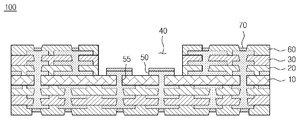
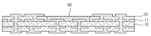
도 2 내지 도 19는 도 1에 따른 인쇄회로기판의 제조 방법을 설명하는 도면이다.
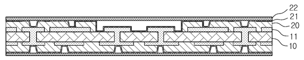
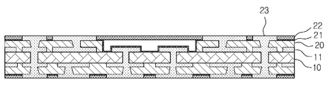
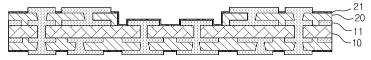
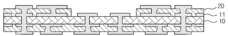
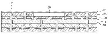
10: 코어층
20: 제1 절연층
30: 제2 절연층
40: 캐비티
50: 도체 패턴
60: 솔더레지스트층
70: 표면처리층
Claims (15)
- 코어층;
상기 코어층 상에 감광성 재질로 형성된 제1 절연층;
상기 제1 절연층 상에 보강재가 함유된 재질로 형성된 제2 절연층; 및
상기 제1 절연층 및 제2 절연층 내에 형성되는 캐비티(cavity)
를 포함하는 인쇄회로기판.
- 제1항에 있어서,
상기 캐비티 내부에 위치하며, 상기 코어층 상에 형성되는 도체 패턴을 더 포함하는 인쇄회로기판.
- 제1항에 있어서,
상기 제2 절연층은,
일면에 동박이 적층된 프리프레그인 인쇄회로기판.
- 제1항에 있어서,
상기 제2 절연층의 상에 형성된 솔더레지스트(SR)층을 더 포함하는 인쇄회로기판.
- 제1항에 있어서,
상기 도체 패턴 상부에 형성되는 표면 처리층을 더 포함하는 인쇄회로기판.
- 코어층을 준비하는 단계;
감광성 재질로 형성된 제1 절연층을 상기 코어층 상에 적층하는 단계;
상기 제1 절연층 내에 제1 캐비티를 형성하는 단계; 및
보강재가 함유된 재질로 형성된 제2 절연층에, 상기 제1 캐비티에 대응되는 제2 캐비티를 형성하는 단계; 및
상기 제2 절연층을 상기 제1 절연층 상에 적층하는 단계를 포함하는 인쇄회로기판 제조 방법.
- 제6항에 있어서,
상기 제1 캐비티는 노광 및 현상 공정을 통해 형성되는 인쇄회로기판 제조 방법.
- 제6항에 있어서,
상기 제1 캐비티는, 상기 코어층 상에 형성된 도체 패턴을 노출시키고,
상기 제1 절연층을 상기 코어층 상에 적층하는 단계 이후에,
상기 제1 캐비티 내부에 상기 도체 패턴을 커버하는 보호층을 적층하는 단계를 더 포함하는 인쇄회로기판 제조 방법.
- 제8항에 있어서,
상기 제2 절연층을 상기 제1 절연층 상부에 적층하는 단계 이후에,
상기 보호층을 제거하는 단계를 더 포함하는 인쇄회로기판 제조 방법.
- 제8항에 있어서,
상기 보호층의 상면의 높이는,
상기 제1 절연층의 상면의 높이 이하인 인쇄회로기판.
- 제6항에 있어서,
상기 제2 절연층은 일면에 동박이 적층된 프리프레그인 인쇄회로기판 제조 방법.
- 제11항에 있어서,
상기 제2 캐비티는 상기 프리프레그 재질 부분이 타발되어 형성되는 적층하는 인쇄회로기판 제조 방법.
- 제6항에 있어서,
상기 제2 절연층은 상기 제1 캐비티의 면적보다 넓은 면적이 타발된 상태로 적층되는 인쇄회로기판 제조 방법.
- 제6항에 있어서,
상기 제2 절연층 상에 솔더레지스트(SR)층을 형성하는 단계를 더 포함하는,
인쇄회로기판 제조 방법.
- 제8항에 있어서,
상기 도체 패턴을 상에 표면 처리층을 형성하는 단계를 더 포함하는 인쇄회로기판 제조 방법.
Priority Applications (3)
| Application Number | Priority Date | Filing Date | Title |
|---|---|---|---|
| KR1020150131215A KR20170033191A (ko) | 2015-09-16 | 2015-09-16 | 인쇄회로기판 및 그 제조 방법 |
| US15/078,452 US20170079142A1 (en) | 2015-09-16 | 2016-03-23 | Printed circuit board and manufacturing method thereof |
| CN201610370758.3A CN106550541A (zh) | 2015-09-16 | 2016-05-30 | 印刷电路板及其制造方法 |
Applications Claiming Priority (1)
| Application Number | Priority Date | Filing Date | Title |
|---|---|---|---|
| KR1020150131215A KR20170033191A (ko) | 2015-09-16 | 2015-09-16 | 인쇄회로기판 및 그 제조 방법 |
Publications (1)
| Publication Number | Publication Date |
|---|---|
| KR20170033191A true KR20170033191A (ko) | 2017-03-24 |
Family
ID=58257667
Family Applications (1)
| Application Number | Title | Priority Date | Filing Date |
|---|---|---|---|
| KR1020150131215A Ceased KR20170033191A (ko) | 2015-09-16 | 2015-09-16 | 인쇄회로기판 및 그 제조 방법 |
Country Status (3)
| Country | Link |
|---|---|
| US (1) | US20170079142A1 (ko) |
| KR (1) | KR20170033191A (ko) |
| CN (1) | CN106550541A (ko) |
Families Citing this family (6)
| Publication number | Priority date | Publication date | Assignee | Title |
|---|---|---|---|---|
| CN110545635B (zh) * | 2018-05-29 | 2021-09-14 | 鹏鼎控股(深圳)股份有限公司 | 多层电路板的制作方法 |
| CN110769598B (zh) * | 2018-07-27 | 2021-11-16 | 宏启胜精密电子(秦皇岛)有限公司 | 内埋式电路板及其制作方法 |
| US20200083154A1 (en) | 2018-09-10 | 2020-03-12 | At&S Austria Technologie & Systemtechnik Aktiengesellschaft | Component Carrier With a Photoimageable Dielectric Layer and a Structured Conductive Layer Being Used as a Mask for Selectively Exposing the Photoimageable Dielectric Layer With Electromagnetic Radiation |
| EP3723459A1 (en) | 2019-04-10 | 2020-10-14 | AT & S Austria Technologie & Systemtechnik Aktiengesellschaft | Component carrier with high passive intermodulation (pim) performance |
| CN111867248A (zh) * | 2019-04-24 | 2020-10-30 | 宏启胜精密电子(秦皇岛)有限公司 | 电路板及其制作方法 |
| CN115190693A (zh) * | 2021-04-02 | 2022-10-14 | 奥特斯奥地利科技与系统技术有限公司 | 部件承载件及其制造方法 |
Citations (1)
| Publication number | Priority date | Publication date | Assignee | Title |
|---|---|---|---|---|
| JPH11186448A (ja) | 1997-12-25 | 1999-07-09 | Kyocera Corp | 積層セラミック回路基板の製造方法 |
Family Cites Families (10)
| Publication number | Priority date | Publication date | Assignee | Title |
|---|---|---|---|---|
| JP2701802B2 (ja) * | 1995-07-17 | 1998-01-21 | 日本電気株式会社 | ベアチップ実装用プリント基板 |
| EP1189271A3 (en) * | 1996-07-12 | 2003-07-16 | Fujitsu Limited | Wiring boards and mounting of semiconductor devices thereon |
| KR100792352B1 (ko) * | 2006-07-06 | 2008-01-08 | 삼성전기주식회사 | 패키지 온 패키지의 바텀기판 및 그 제조방법 |
| JP5013973B2 (ja) * | 2007-05-31 | 2012-08-29 | 株式会社メイコー | プリント配線板及びその製造方法、並びに、このプリント配線板を用いた電子部品収容基板及びその製造方法 |
| KR100869049B1 (ko) * | 2007-06-25 | 2008-11-17 | 대덕전자 주식회사 | 자외선 감광 폴리이미드 라미네이션을 적용한 세미애디티브 기판 제조 방법 |
| TW200952142A (en) * | 2008-06-13 | 2009-12-16 | Phoenix Prec Technology Corp | Package substrate having embedded semiconductor chip and fabrication method thereof |
| US8609992B2 (en) * | 2009-12-24 | 2013-12-17 | Dai Nippon Printing Co., Ltd. | Circuit board, manufacturing method of circuit board, suspension substrate, suspension, device-mounted suspension, and hard disk drive |
| KR101472633B1 (ko) * | 2012-10-16 | 2014-12-15 | 삼성전기주식회사 | 하이브리드 적층기판, 그 제조방법 및 패키지 기판 |
| TW201446083A (zh) * | 2013-05-17 | 2014-12-01 | Microcosm Technology Co Ltd | 垂直導電單元及其製造方法 |
| KR102167597B1 (ko) * | 2014-01-22 | 2020-10-19 | 엘지이노텍 주식회사 | 임베디드 인쇄회로기판 |
-
2015
- 2015-09-16 KR KR1020150131215A patent/KR20170033191A/ko not_active Ceased
-
2016
- 2016-03-23 US US15/078,452 patent/US20170079142A1/en not_active Abandoned
- 2016-05-30 CN CN201610370758.3A patent/CN106550541A/zh active Pending
Patent Citations (1)
| Publication number | Priority date | Publication date | Assignee | Title |
|---|---|---|---|---|
| JPH11186448A (ja) | 1997-12-25 | 1999-07-09 | Kyocera Corp | 積層セラミック回路基板の製造方法 |
Also Published As
| Publication number | Publication date |
|---|---|
| CN106550541A (zh) | 2017-03-29 |
| US20170079142A1 (en) | 2017-03-16 |
Similar Documents
| Publication | Publication Date | Title |
|---|---|---|
| KR102472945B1 (ko) | 인쇄회로기판, 반도체 패키지 및 그 제조방법 | |
| US8835773B2 (en) | Wiring board and method of manufacturing the same | |
| US8207450B2 (en) | Printed circuit board comprising metal bumps integrated with connection pads | |
| KR20170033191A (ko) | 인쇄회로기판 및 그 제조 방법 | |
| KR102333091B1 (ko) | 인쇄회로기판 및 인쇄회로기판의 제조 방법 | |
| KR20000047653A (ko) | 두 개의 신호 플레인과 한 개의 전원 플레인을 갖는 회로기판 | |
| KR20090056824A (ko) | 배선 기판 및 전자 부품 장치 | |
| KR20120047826A (ko) | 다층 배선기판 | |
| KR20180070276A (ko) | 인쇄회로기판, 패키지 및 인쇄회로기판의 제조방법 | |
| JP2015216293A (ja) | 配線基板の製造方法及び配線基板 | |
| JP2015185828A (ja) | 電子部品内蔵多層配線板およびその製造方法 | |
| CN105282972A (zh) | 器件内置型印刷电路板、半导体封装及其制造方法 | |
| CN102026489B (zh) | 电路板的制作方法 | |
| KR101222828B1 (ko) | 코어리스 기판의 제조방법 | |
| KR20140039921A (ko) | 인쇄회로기판의 제조 방법 | |
| KR20120120789A (ko) | 인쇄회로기판의 제조방법 | |
| KR101501902B1 (ko) | 금속 포스트를 구비한 인쇄회로기판 및 이의 제조 방법 | |
| KR20180013017A (ko) | 인쇄회로기판 | |
| KR102333097B1 (ko) | 인쇄회로기판, 그 제조방법, 및 전자부품 모듈 | |
| KR101212526B1 (ko) | 보드온칩 패키지, 이를 위한 인쇄회로기판 및 제조 방법 | |
| KR101480557B1 (ko) | 인쇄회로기판 및 그 제조방법 | |
| KR20090044023A (ko) | 인쇄회로기판 제조방법 | |
| KR20120015397A (ko) | 인쇄회로기판의 제조 방법 | |
| KR100688865B1 (ko) | 도금에 의한 범프 형성 방법 및 이를 이용한 인쇄회로기판제조방법 | |
| KR100815322B1 (ko) | 인쇄회로기판 및 그 제조방법 |
Legal Events
| Date | Code | Title | Description |
|---|---|---|---|
| PA0109 | Patent application |
Patent event code: PA01091R01D Comment text: Patent Application Patent event date: 20150916 |
|
| PG1501 | Laying open of application | ||
| A201 | Request for examination | ||
| PA0201 | Request for examination |
Patent event code: PA02012R01D Patent event date: 20200811 Comment text: Request for Examination of Application Patent event code: PA02011R01I Patent event date: 20150916 Comment text: Patent Application |
|
| E902 | Notification of reason for refusal | ||
| PE0902 | Notice of grounds for rejection |
Comment text: Notification of reason for refusal Patent event date: 20211015 Patent event code: PE09021S01D |
|
| AMND | Amendment | ||
| E601 | Decision to refuse application | ||
| PE0601 | Decision on rejection of patent |
Patent event date: 20220415 Comment text: Decision to Refuse Application Patent event code: PE06012S01D Patent event date: 20211015 Comment text: Notification of reason for refusal Patent event code: PE06011S01I |
|
| X091 | Application refused [patent] | ||
| AMND | Amendment | ||
| PX0901 | Re-examination |
Patent event code: PX09011S01I Patent event date: 20220415 Comment text: Decision to Refuse Application Patent event code: PX09012R01I Patent event date: 20211130 Comment text: Amendment to Specification, etc. |
|
| PX0601 | Decision of rejection after re-examination |
Comment text: Decision to Refuse Application Patent event code: PX06014S01D Patent event date: 20220615 Comment text: Amendment to Specification, etc. Patent event code: PX06012R01I Patent event date: 20220516 Comment text: Decision to Refuse Application Patent event code: PX06011S01I Patent event date: 20220415 Comment text: Amendment to Specification, etc. Patent event code: PX06012R01I Patent event date: 20211130 Comment text: Notification of reason for refusal Patent event code: PX06013S01I Patent event date: 20211015 |
|
| X601 | Decision of rejection after re-examination |