KR20170034067A - 유기 발광 표시 장치 - Google Patents
유기 발광 표시 장치 Download PDFInfo
- Publication number
- KR20170034067A KR20170034067A KR1020150132270A KR20150132270A KR20170034067A KR 20170034067 A KR20170034067 A KR 20170034067A KR 1020150132270 A KR1020150132270 A KR 1020150132270A KR 20150132270 A KR20150132270 A KR 20150132270A KR 20170034067 A KR20170034067 A KR 20170034067A
- Authority
- KR
- South Korea
- Prior art keywords
- layer
- light emitting
- hole transport
- mixed
- transport layer
- Prior art date
- Legal status (The legal status is an assumption and is not a legal conclusion. Google has not performed a legal analysis and makes no representation as to the accuracy of the status listed.)
- Ceased
Links
Images




Classifications
-
- H—ELECTRICITY
- H10—SEMICONDUCTOR DEVICES; ELECTRIC SOLID-STATE DEVICES NOT OTHERWISE PROVIDED FOR
- H10K—ORGANIC ELECTRIC SOLID-STATE DEVICES
- H10K59/00—Integrated devices, or assemblies of multiple devices, comprising at least one organic light-emitting element covered by group H10K50/00
- H10K59/30—Devices specially adapted for multicolour light emission
- H10K59/32—Stacked devices having two or more layers, each emitting at different wavelengths
-
- H01L51/5056—
-
- H01L27/3225—
-
- H01L51/5004—
-
- H01L51/5008—
-
- H01L51/5016—
-
- H01L51/5278—
-
- H—ELECTRICITY
- H10—SEMICONDUCTOR DEVICES; ELECTRIC SOLID-STATE DEVICES NOT OTHERWISE PROVIDED FOR
- H10K—ORGANIC ELECTRIC SOLID-STATE DEVICES
- H10K30/00—Organic devices sensitive to infrared radiation, light, electromagnetic radiation of shorter wavelength or corpuscular radiation
- H10K30/80—Constructional details
- H10K30/865—Intermediate layers comprising a mixture of materials of the adjoining active layers
-
- H—ELECTRICITY
- H10—SEMICONDUCTOR DEVICES; ELECTRIC SOLID-STATE DEVICES NOT OTHERWISE PROVIDED FOR
- H10K—ORGANIC ELECTRIC SOLID-STATE DEVICES
- H10K50/00—Organic light-emitting devices
- H10K50/10—OLEDs or polymer light-emitting diodes [PLED]
- H10K50/11—OLEDs or polymer light-emitting diodes [PLED] characterised by the electroluminescent [EL] layers
-
- H—ELECTRICITY
- H10—SEMICONDUCTOR DEVICES; ELECTRIC SOLID-STATE DEVICES NOT OTHERWISE PROVIDED FOR
- H10K—ORGANIC ELECTRIC SOLID-STATE DEVICES
- H10K50/00—Organic light-emitting devices
- H10K50/10—OLEDs or polymer light-emitting diodes [PLED]
- H10K50/11—OLEDs or polymer light-emitting diodes [PLED] characterised by the electroluminescent [EL] layers
- H10K50/125—OLEDs or polymer light-emitting diodes [PLED] characterised by the electroluminescent [EL] layers specially adapted for multicolour light emission, e.g. for emitting white light
- H10K50/13—OLEDs or polymer light-emitting diodes [PLED] characterised by the electroluminescent [EL] layers specially adapted for multicolour light emission, e.g. for emitting white light comprising stacked EL layers within one EL unit
-
- H—ELECTRICITY
- H10—SEMICONDUCTOR DEVICES; ELECTRIC SOLID-STATE DEVICES NOT OTHERWISE PROVIDED FOR
- H10K—ORGANIC ELECTRIC SOLID-STATE DEVICES
- H10K50/00—Organic light-emitting devices
- H10K50/10—OLEDs or polymer light-emitting diodes [PLED]
- H10K50/14—Carrier transporting layers
- H10K50/15—Hole transporting layers
-
- H—ELECTRICITY
- H10—SEMICONDUCTOR DEVICES; ELECTRIC SOLID-STATE DEVICES NOT OTHERWISE PROVIDED FOR
- H10K—ORGANIC ELECTRIC SOLID-STATE DEVICES
- H10K50/00—Organic light-emitting devices
- H10K50/10—OLEDs or polymer light-emitting diodes [PLED]
- H10K50/14—Carrier transporting layers
- H10K50/15—Hole transporting layers
- H10K50/156—Hole transporting layers comprising a multilayered structure
-
- H—ELECTRICITY
- H10—SEMICONDUCTOR DEVICES; ELECTRIC SOLID-STATE DEVICES NOT OTHERWISE PROVIDED FOR
- H10K—ORGANIC ELECTRIC SOLID-STATE DEVICES
- H10K50/00—Organic light-emitting devices
- H10K50/10—OLEDs or polymer light-emitting diodes [PLED]
- H10K50/19—Tandem OLEDs
-
- H—ELECTRICITY
- H10—SEMICONDUCTOR DEVICES; ELECTRIC SOLID-STATE DEVICES NOT OTHERWISE PROVIDED FOR
- H10K—ORGANIC ELECTRIC SOLID-STATE DEVICES
- H10K50/00—Organic light-emitting devices
- H10K50/80—Constructional details
- H10K50/85—Arrangements for extracting light from the devices
- H10K50/852—Arrangements for extracting light from the devices comprising a resonant cavity structure, e.g. Bragg reflector pair
-
- H—ELECTRICITY
- H10—SEMICONDUCTOR DEVICES; ELECTRIC SOLID-STATE DEVICES NOT OTHERWISE PROVIDED FOR
- H10K—ORGANIC ELECTRIC SOLID-STATE DEVICES
- H10K59/00—Integrated devices, or assemblies of multiple devices, comprising at least one organic light-emitting element covered by group H10K50/00
- H10K59/10—OLED displays
- H10K59/12—Active-matrix OLED [AMOLED] displays
-
- H—ELECTRICITY
- H10—SEMICONDUCTOR DEVICES; ELECTRIC SOLID-STATE DEVICES NOT OTHERWISE PROVIDED FOR
- H10K—ORGANIC ELECTRIC SOLID-STATE DEVICES
- H10K59/00—Integrated devices, or assemblies of multiple devices, comprising at least one organic light-emitting element covered by group H10K50/00
- H10K59/80—Constructional details
- H10K59/875—Arrangements for extracting light from the devices
- H10K59/876—Arrangements for extracting light from the devices comprising a resonant cavity structure, e.g. Bragg reflector pair
-
- H01L2227/32—
-
- H—ELECTRICITY
- H10—SEMICONDUCTOR DEVICES; ELECTRIC SOLID-STATE DEVICES NOT OTHERWISE PROVIDED FOR
- H10K—ORGANIC ELECTRIC SOLID-STATE DEVICES
- H10K2101/00—Properties of the organic materials covered by group H10K85/00
- H10K2101/10—Triplet emission
-
- H—ELECTRICITY
- H10—SEMICONDUCTOR DEVICES; ELECTRIC SOLID-STATE DEVICES NOT OTHERWISE PROVIDED FOR
- H10K—ORGANIC ELECTRIC SOLID-STATE DEVICES
- H10K2101/00—Properties of the organic materials covered by group H10K85/00
- H10K2101/30—Highest occupied molecular orbital [HOMO], lowest unoccupied molecular orbital [LUMO] or Fermi energy values
-
- H—ELECTRICITY
- H10—SEMICONDUCTOR DEVICES; ELECTRIC SOLID-STATE DEVICES NOT OTHERWISE PROVIDED FOR
- H10K—ORGANIC ELECTRIC SOLID-STATE DEVICES
- H10K2101/00—Properties of the organic materials covered by group H10K85/00
- H10K2101/40—Interrelation of parameters between multiple constituent active layers or sublayers, e.g. HOMO values in adjacent layers
-
- H—ELECTRICITY
- H10—SEMICONDUCTOR DEVICES; ELECTRIC SOLID-STATE DEVICES NOT OTHERWISE PROVIDED FOR
- H10K—ORGANIC ELECTRIC SOLID-STATE DEVICES
- H10K2102/00—Constructional details relating to the organic devices covered by this subclass
- H10K2102/301—Details of OLEDs
- H10K2102/351—Thickness
-
- H—ELECTRICITY
- H10—SEMICONDUCTOR DEVICES; ELECTRIC SOLID-STATE DEVICES NOT OTHERWISE PROVIDED FOR
- H10K—ORGANIC ELECTRIC SOLID-STATE DEVICES
- H10K59/00—Integrated devices, or assemblies of multiple devices, comprising at least one organic light-emitting element covered by group H10K50/00
- H10K59/80—Constructional details
- H10K59/805—Electrodes
- H10K59/8052—Cathodes
- H10K59/80524—Transparent cathodes, e.g. comprising thin metal layers
Landscapes
- Physics & Mathematics (AREA)
- Optics & Photonics (AREA)
- Electromagnetism (AREA)
- Engineering & Computer Science (AREA)
- Microelectronics & Electronic Packaging (AREA)
- Electroluminescent Light Sources (AREA)
Abstract
Description
도 2는 본 발명의 일 실시예에 따른 유기 발광 표시 장치의 주요 구성 요소를 나타낸 단면도이다.
도 3은 본 발명의 일 실시예에 따른 유기 발광 표시 장치의 주요 구성 요소의 에너지 밴드 다이어그램을 나타낸 도면이다.
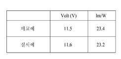
도 4는 비교예 및 본 발명의 일 실시예에 따른 유기 발광 표시 장치의 구동 전압 및 발광 효율을 나타낸 표이다.
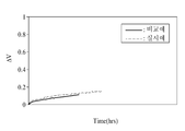
도 5는 비교예 및 본 발명의 일 실시예에 따른 유기 발광 표시 장치의 시간에 따른 구동 전압의 변화를 나타낸 그래프이다.
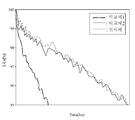
도 6a 및 도 6b는 비교예 및 본 발명의 일 실시예에 따른 유기 발광 표시 장치의 수명을 나타낸 그래프이다.
도 7은 본 발명의 다른 실시예에 따른 유기 발광 표시 장치의 주요 구성 요소를 나타낸 단면도이다.
도 8은 도 7의 정공 수송층을 제조하는 공증착(co-depositon)법을 모식화한 도면이다.
도 9은 본 발명의 또 다른 실시예에 따른 유기 발광 표시 장치의 주요 구성 요소를 나타낸 단면도이다.
도 10a는 비교예 및 본 발명의 또 다른 실시예에 따른 유기 발광 표시 장치의 시간에 따른 구동 전압의 변화를 나타낸 그래프이다.
도 10b는 비교예 및 본 발명의 또 다른 실시예에 따른 유기 발광 표시 장치의 시간에 따른 수명을 나타낸 그래프이다.
100: 기판
300: 박막 트랜지스터
ED: 발광 소자
400: 애노드
500: 발광부
600: 캐소드
511, 521, 531, 1511: 정공 수송층
511a: 제1 물질
511b: 제2 물질
512, 522, 532, 1512: 발광층
513, 523, 533, 1513: 전자 수송층
540, 440: 전하 생성층
710, 720: 증착원
Claims (20)
- 애노드와 캐소드 사이에, 발광부를 포함하는 유기 발광 표시 장치에 있어서,
상기 발광부는 제1 발광층, 및 제1 물질과 제2 물질로 이루어진 제1 정공 수송층을 포함하고,
상기 제1 물질은 상기 제1 정공 수송층으로부터 상기 제1 발광층으로의 정공의 이동이 향상되도록 상기 제2 물질 대비 정공 이동도가 큰 물질이고, 상기 제2 물질은 상기 제1 발광층으로부터 상기 제1 정공 수송층으로의 전자의 이동이 감소되도록, 상기 제1 물질 대비 삼중항 에너지 레벨이 높은 물질인, 유기 발광 표시 장치. - 제1 항에 있어서,
상기 제2 물질은, 상기 제1 정공 수송층의 계면에 정공이 축적되는 것이 최소화되도록, 상기 제1 물질 대비 HOMO레벨이 낮은 물질인, 유기 발광 표시 장치. - 제2 항에 있어서,
상기 제1 발광층과 상기 제1 정공 수송층 사이에 추가 정공 수송층이 더 포함된 유기 발광 표시 장치. - 제2 항에 있어서,
상기 제1 정공 수송층은 단일층인, 유기 발광 표시 장치. - 제4 항에 있어서,
상기 제1 물질과 상기 제2 물질의 중량의 합을 100wt%라고 했을 때,
상기 제1 물질은, 50wt% 이상 90wt% 이하이고,
상기 제2 물질은, 10wt% 이상 50wt% 이하인, 유기 발광 표시 장치. - 제5 항에 있어서,
상기 제1 정공 수송층의 두께는, 상기 애노드와 상기 캐소드 사이의 거리에 의한 상기 제1 발광층으로부터 발광된 광의 미세-공진이 최적화되도록, 70㎚ 이상 150㎚ 이하인, 유기 발광 표시 장치. - 제2 항에 있어서,
상기 제1 정공 수송층은, 상기 제1 물질과 상기 제2 물질이 혼합된 혼합층 및, 상기 제1 물질 또는 상기 제2 물질로만 이루어진 적어도 하나의 미-혼합층을 포함하는, 유기 발광 표시 장치. - 제7 항에 있어서,
상기 미-혼합층은, 상기 제1 물질로만 이루어진 제1 미-혼합층 및 상기 제2 물질로만 이루어진 제2 미-혼합층을 포함하고,
상기 제1 미-혼합층은 상대적으로 상기 애노드에 가장 가깝게 배치되며 상기 제1 발광층으로의 정공의 이동을 돕는 역할을 하고, 상기 제2 미-혼합층은 상대적으로 상기 제1 발광층에 가장 가깝게 배치되며 상기 제1 발광층으로부터 전자가 이동되는 것을 막는 역할을 하는, 유기 발광 표시 장치. - 제8 항에 있어서,
상기 혼합층에 포함된 상기 제1 물질과 상기 제2 물질의 중량의 합을 100wt%라고 했을 때,
상기 제1 물질은 50wt% 이상 90wt% 이하이고,
상기 제2 물질은 10wt% 이상 50wt% 이하인, 유기 발광 표시 장치. - 제8 항에 있어서,
상기 제1 미-혼합층의 두께 또는 상기 제2 미-혼합층의 두께는, 상기 혼합층의 두께 대비 40% 이하인, 유기 발광 표시 장치. - 제2 항에 있어서,
상기 제1 물질의 정공 이동도는, 1×10⁻⁴㎠/Vs 이상인, 유기 발광 표시 장치. - 제2 항에 있어서,
상기 제2 물질의 삼중항 에너지 레벨은, -2.7eV 이상 -2.6eV 이하이고,
상기 제2 물질의 HOMO레벨은, -5.2eV 이상 -4.7eV 이하인, 유기 발광 표시 장치. - 제2 항에 있어서,
상기 발광부로부터 청색의 빛이 발광되도록, 상기 제1 발광층으로부터 발광된 광의 피크 파장은, 440nm 이상 480nm 이하인, 유기 발광 표시 장치. - 제2 항에 있어서,
상기 발광부로부터 백색의 빛이 발광되도록 상기 발광부는,
상기 제1 발광층 및 상기 제1 정공 수송층을 포함하는 제1 스택;
상기 제1 스택 상에, 제2 발광층을 포함하는 제2 스택; 및
상기 제2 스택 상에, 제3 발광층을 포함하는 제3 스택을 포함하고,
상기 제1 발광층과 상기 제3 발광층으로부터 발광된 광의 피크 파장은 440nm 이상 480nm 이하이고,
상기 제2 발광층으로부터 발광된 광의 피크 파장은, 540nm 이상 580nm 이하인, 유기 발광 표시 장치. - 애노드와 캐소드 사이에, 적어도 하나의 발광층 및 적어도 하나의 정공 수송층을 포함하는 유기 발광 표시 장치에 있어서,
상기 적어도 하나의 정공 수송층은, 서로 상이한 특성의 2종 물질을 포함하는 혼합 구조(mixed structure)로 구성된, 유기 발광 표시 장치. - 제15 항에 있어서,
상기 적어도 하나의 정공 수송층은, 정공 이동도가 상대적으로 큰 제1 물질 및 삼중항 에너지 레벨이 상대적으로 높은 제2 물질이 혼합된 구조인, 유기 발광 표시 장치. - 제16 항에 있어서,
상기 제2 물질의 HOMO레벨은, 상기 제1 물질의 HOMO레벨보다 낮은, 유기 발광 표시 장치. - 제17 항에 있어서,
상기 적어도 하나의 정공 수송층에 포함된 상기 제1 물질 및 상기 제2 물질의 중량의 합을 100wt%라고 했을 때,
상기 제1 물질은 50wt% 이상 90wt% 이하이고,
상기 제2 물질은 10wt% 이상 50wt% 이하인, 유기 발광 표시 장치. - 제17 항에 있어서,
상기 제1 물질의 정공 이동도는, 1×10⁻⁴㎠/Vs 이상인, 유기 발광 표시 장치. - 제17 항에 있어서,
상기 제2 물질의 삼중항 에너지 레벨은, -2.7eV 이상 -2.6eV 이하이고,
상기 제2 물질의 HOMO레벨은, -5.2eV 이상 -4.7eV 이하인, 유기 발광 표시 장치.
Priority Applications (5)
| Application Number | Priority Date | Filing Date | Title |
|---|---|---|---|
| KR1020150132270A KR20170034067A (ko) | 2015-09-18 | 2015-09-18 | 유기 발광 표시 장치 |
| US15/189,739 US9806276B2 (en) | 2015-09-18 | 2016-06-22 | Organic light emitting display apparatus |
| EP16176568.0A EP3144991B1 (en) | 2015-09-18 | 2016-06-28 | Organic light emitting display apparatus |
| CN201610507431.6A CN106549108B (zh) | 2015-09-18 | 2016-06-30 | 有机发光显示装置 |
| KR1020220018723A KR102422769B1 (ko) | 2015-09-18 | 2022-02-14 | 유기 발광 표시 장치 |
Applications Claiming Priority (1)
| Application Number | Priority Date | Filing Date | Title |
|---|---|---|---|
| KR1020150132270A KR20170034067A (ko) | 2015-09-18 | 2015-09-18 | 유기 발광 표시 장치 |
Related Child Applications (1)
| Application Number | Title | Priority Date | Filing Date |
|---|---|---|---|
| KR1020220018723A Division KR102422769B1 (ko) | 2015-09-18 | 2022-02-14 | 유기 발광 표시 장치 |
Publications (1)
| Publication Number | Publication Date |
|---|---|
| KR20170034067A true KR20170034067A (ko) | 2017-03-28 |
Family
ID=56292499
Family Applications (2)
| Application Number | Title | Priority Date | Filing Date |
|---|---|---|---|
| KR1020150132270A Ceased KR20170034067A (ko) | 2015-09-18 | 2015-09-18 | 유기 발광 표시 장치 |
| KR1020220018723A Active KR102422769B1 (ko) | 2015-09-18 | 2022-02-14 | 유기 발광 표시 장치 |
Family Applications After (1)
| Application Number | Title | Priority Date | Filing Date |
|---|---|---|---|
| KR1020220018723A Active KR102422769B1 (ko) | 2015-09-18 | 2022-02-14 | 유기 발광 표시 장치 |
Country Status (4)
| Country | Link |
|---|---|
| US (1) | US9806276B2 (ko) |
| EP (1) | EP3144991B1 (ko) |
| KR (2) | KR20170034067A (ko) |
| CN (1) | CN106549108B (ko) |
Cited By (1)
| Publication number | Priority date | Publication date | Assignee | Title |
|---|---|---|---|---|
| KR20220085109A (ko) * | 2020-12-14 | 2022-06-22 | 삼성디스플레이 주식회사 | 표시 장치 및 그 제조 방법 |
Families Citing this family (8)
| Publication number | Priority date | Publication date | Assignee | Title |
|---|---|---|---|---|
| KR102377466B1 (ko) * | 2015-10-29 | 2022-03-21 | 엘지디스플레이 주식회사 | 유기 발광 표시 장치 |
| CN109524438B (zh) * | 2018-11-13 | 2021-01-15 | 武汉华星光电半导体显示技术有限公司 | 一种电致发光显示器件及其制备方法 |
| US11056540B2 (en) | 2019-03-12 | 2021-07-06 | Universal Display Corporation | Plasmonic PHOLED arrangement for displays |
| JP7500164B2 (ja) * | 2019-05-07 | 2024-06-17 | キヤノン株式会社 | 有機発光素子、それを有する表示装置、撮像装置、照明装置、移動体 |
| KR102821745B1 (ko) * | 2020-08-20 | 2025-06-18 | 삼성디스플레이 주식회사 | 발광 소자 및 이를 포함한 전자 장치 |
| US12310166B2 (en) | 2021-02-24 | 2025-05-20 | Boe Technology Group Co., Ltd. | Light-emitting device, manufacturing method thereof, and display device |
| CN113437231B (zh) * | 2021-06-22 | 2022-11-08 | 云谷(固安)科技有限公司 | 显示面板及显示装置 |
| JP7631252B2 (ja) * | 2022-03-31 | 2025-02-18 | キヤノン株式会社 | 発光装置、表示装置、撮像装置、及び、電子機器 |
Family Cites Families (18)
| Publication number | Priority date | Publication date | Assignee | Title |
|---|---|---|---|---|
| US20040209116A1 (en) * | 2003-04-21 | 2004-10-21 | Xiaofan Ren | Organic light emitting devices with wide gap host materials |
| JP4086817B2 (ja) * | 2004-07-20 | 2008-05-14 | キヤノン株式会社 | 有機el素子 |
| US9070884B2 (en) * | 2005-04-13 | 2015-06-30 | Universal Display Corporation | Hybrid OLED having phosphorescent and fluorescent emitters |
| WO2011065138A1 (ja) * | 2009-11-27 | 2011-06-03 | シャープ株式会社 | 有機エレクトロルミネッセンス素子、およびその製造方法、ならびに有機エレクトロルミネッセンス表示装置 |
| JP6056763B2 (ja) | 2011-10-21 | 2017-01-11 | コニカミノルタ株式会社 | 有機エレクトロルミネッセンス素子 |
| WO2013118812A1 (ja) | 2012-02-10 | 2013-08-15 | 出光興産株式会社 | 有機エレクトロルミネッセンス素子 |
| US9054323B2 (en) * | 2012-03-15 | 2015-06-09 | Universal Display Corporation | Secondary hole transporting layer with diarylamino-phenyl-carbazole compounds |
| KR101950836B1 (ko) * | 2012-05-22 | 2019-02-22 | 엘지디스플레이 주식회사 | 유기 발광 소자 및 그의 제조 방법 |
| TWI527211B (zh) * | 2012-12-28 | 2016-03-21 | Lg顯示器股份有限公司 | 有機發光顯示裝置及其製造方法 |
| KR20140140417A (ko) | 2013-05-29 | 2014-12-09 | 삼성디스플레이 주식회사 | 유기 발광 소자 |
| DE102013017361B4 (de) * | 2013-10-18 | 2023-05-04 | Pictiva Displays International Limited | Organisches Licht emittierendes Bauelement und Verfahren zur Herstellung eines organischen Licht ermittierenden Bauelements |
| KR102053443B1 (ko) | 2013-10-23 | 2019-12-06 | 엘지디스플레이 주식회사 | 유기전계발광소자 |
| US9768403B2 (en) * | 2013-10-30 | 2017-09-19 | Sharp Kabushiki Kaisha | Organic electroluminescent element and organic electroluminescent display panel |
| DE102014100993A1 (de) * | 2013-12-05 | 2015-06-11 | Osram Opto Semiconductors Gmbh | Organisches lichtemittierendes Bauelement und Verfahren zur Herstellung des organischen lichtemittierenden Bauelements |
| JP5905916B2 (ja) * | 2013-12-26 | 2016-04-20 | 出光興産株式会社 | 有機エレクトロルミネッセンス素子および電子機器 |
| KR102221106B1 (ko) * | 2014-01-17 | 2021-03-02 | 삼성디스플레이 주식회사 | 유기 발광 소자 |
| JP6580553B2 (ja) * | 2014-02-18 | 2019-09-25 | 保土谷化学工業株式会社 | ベンゾフロインドール誘導体および有機エレクトロルミネッセンス素子 |
| JP2017123352A (ja) * | 2014-03-31 | 2017-07-13 | 出光興産株式会社 | 有機エレクトロルミネッセンス素子および電子機器 |
-
2015
- 2015-09-18 KR KR1020150132270A patent/KR20170034067A/ko not_active Ceased
-
2016
- 2016-06-22 US US15/189,739 patent/US9806276B2/en active Active
- 2016-06-28 EP EP16176568.0A patent/EP3144991B1/en active Active
- 2016-06-30 CN CN201610507431.6A patent/CN106549108B/zh active Active
-
2022
- 2022-02-14 KR KR1020220018723A patent/KR102422769B1/ko active Active
Cited By (2)
| Publication number | Priority date | Publication date | Assignee | Title |
|---|---|---|---|---|
| KR20220085109A (ko) * | 2020-12-14 | 2022-06-22 | 삼성디스플레이 주식회사 | 표시 장치 및 그 제조 방법 |
| US12538696B2 (en) | 2020-12-14 | 2026-01-27 | Samsung Display Co., Ltd. | Display apparatus and method of manufacturing the same |
Also Published As
| Publication number | Publication date |
|---|---|
| KR102422769B1 (ko) | 2022-07-18 |
| CN106549108B (zh) | 2019-01-04 |
| EP3144991B1 (en) | 2021-10-13 |
| KR20220024355A (ko) | 2022-03-03 |
| EP3144991A1 (en) | 2017-03-22 |
| CN106549108A (zh) | 2017-03-29 |
| US20170084855A1 (en) | 2017-03-23 |
| US9806276B2 (en) | 2017-10-31 |
Similar Documents
| Publication | Publication Date | Title |
|---|---|---|
| KR102422769B1 (ko) | 유기 발광 표시 장치 | |
| US10622411B2 (en) | Organic light-emitting device and organic light-emitting display device using the same | |
| KR102750999B1 (ko) | 유기 발광 소자 및 이를 포함하는 유기 발광 표시 장치 | |
| US9761823B2 (en) | Organic light emitting display device | |
| CN107689422B (zh) | 有机发光二极管及包括其的显示装置 | |
| KR102863119B1 (ko) | 유기 발광 소자 및 그를 이용한 유기 발광 표시 장치 | |
| US8878171B2 (en) | Organic light emitting display device | |
| KR20160066234A (ko) | 유기 발광 표시 장치 및 이의 제조 방법 | |
| KR20170066898A (ko) | 유기 발광 표시 장치 | |
| KR20190057749A (ko) | 유기 발광 표시 장치 및 이의 제조 방법 | |
| US9692002B2 (en) | Organic light emitting display device | |
| US20230217670A1 (en) | Light-emitting device and light-emitting display device including the same | |
| KR102672009B1 (ko) | 유기 발광 소자 및 이를 포함하는 유기 발광 표시 장치 | |
| KR20170123896A (ko) | 유기 발광 표시 장치 | |
| KR20150041314A (ko) | 유기전계 발광소자 및 그 제조방법 | |
| KR102255861B1 (ko) | 유기 발광 표시 장치 |
Legal Events
| Date | Code | Title | Description |
|---|---|---|---|
| PA0109 | Patent application |
St.27 status event code: A-0-1-A10-A12-nap-PA0109 |
|
| PG1501 | Laying open of application |
St.27 status event code: A-1-1-Q10-Q12-nap-PG1501 |
|
| P22-X000 | Classification modified |
St.27 status event code: A-2-2-P10-P22-nap-X000 |
|
| A201 | Request for examination | ||
| PA0201 | Request for examination |
St.27 status event code: A-1-2-D10-D11-exm-PA0201 |
|
| E902 | Notification of reason for refusal | ||
| PE0902 | Notice of grounds for rejection |
St.27 status event code: A-1-2-D10-D21-exm-PE0902 |
|
| E13-X000 | Pre-grant limitation requested |
St.27 status event code: A-2-3-E10-E13-lim-X000 |
|
| P11-X000 | Amendment of application requested |
St.27 status event code: A-2-2-P10-P11-nap-X000 |
|
| P13-X000 | Application amended |
St.27 status event code: A-2-2-P10-P13-nap-X000 |
|
| E601 | Decision to refuse application | ||
| PE0601 | Decision on rejection of patent |
St.27 status event code: N-2-6-B10-B15-exm-PE0601 |
|
| E13-X000 | Pre-grant limitation requested |
St.27 status event code: A-2-3-E10-E13-lim-X000 |
|
| P11-X000 | Amendment of application requested |
St.27 status event code: A-2-2-P10-P11-nap-X000 |
|
| E601 | Decision to refuse application | ||
| E801 | Decision on dismissal of amendment | ||
| PE0601 | Decision on rejection of patent |
St.27 status event code: N-2-6-B10-B15-exm-PE0601 |
|
| PE0801 | Dismissal of amendment |
St.27 status event code: A-2-2-P10-P12-nap-PE0801 |
|
| T11-X000 | Administrative time limit extension requested |
St.27 status event code: U-3-3-T10-T11-oth-X000 |
|
| T13-X000 | Administrative time limit extension granted |
St.27 status event code: U-3-3-T10-T13-oth-X000 |
|
| A107 | Divisional application of patent | ||
| PA0107 | Divisional application |
St.27 status event code: A-0-1-A10-A18-div-PA0107 St.27 status event code: A-0-1-A10-A16-div-PA0107 |
|
| P22-X000 | Classification modified |
St.27 status event code: A-2-2-P10-P22-nap-X000 |
|
| P22-X000 | Classification modified |
St.27 status event code: A-2-2-P10-P22-nap-X000 |
|
| P22-X000 | Classification modified |
St.27 status event code: A-2-2-P10-P22-nap-X000 |
|
| P22-X000 | Classification modified |
St.27 status event code: A-2-2-P10-P22-nap-X000 |