KR20170036721A - 도전 재료 - Google Patents
도전 재료 Download PDFInfo
- Publication number
- KR20170036721A KR20170036721A KR1020177004503A KR20177004503A KR20170036721A KR 20170036721 A KR20170036721 A KR 20170036721A KR 1020177004503 A KR1020177004503 A KR 1020177004503A KR 20177004503 A KR20177004503 A KR 20177004503A KR 20170036721 A KR20170036721 A KR 20170036721A
- Authority
- KR
- South Korea
- Prior art keywords
- particles
- conductive
- resin core
- insulating
- conductive layer
- Prior art date
- Legal status (The legal status is an assumption and is not a legal conclusion. Google has not performed a legal analysis and makes no representation as to the accuracy of the status listed.)
- Ceased
Links
Images


Classifications
-
- H—ELECTRICITY
- H01—ELECTRIC ELEMENTS
- H01R—ELECTRICALLY-CONDUCTIVE CONNECTIONS; STRUCTURAL ASSOCIATIONS OF A PLURALITY OF MUTUALLY-INSULATED ELECTRICAL CONNECTING ELEMENTS; COUPLING DEVICES; CURRENT COLLECTORS
- H01R4/00—Electrically-conductive connections between two or more conductive members in direct contact, i.e. touching one another; Means for effecting or maintaining such contact; Electrically-conductive connections having two or more spaced connecting locations for conductors and using contact members penetrating insulation
- H01R4/10—Electrically-conductive connections between two or more conductive members in direct contact, i.e. touching one another; Means for effecting or maintaining such contact; Electrically-conductive connections having two or more spaced connecting locations for conductors and using contact members penetrating insulation effected solely by twisting, wrapping, bending, crimping, or other permanent deformation
- H01R4/18—Electrically-conductive connections between two or more conductive members in direct contact, i.e. touching one another; Means for effecting or maintaining such contact; Electrically-conductive connections having two or more spaced connecting locations for conductors and using contact members penetrating insulation effected solely by twisting, wrapping, bending, crimping, or other permanent deformation by crimping
- H01R4/188—Electrically-conductive connections between two or more conductive members in direct contact, i.e. touching one another; Means for effecting or maintaining such contact; Electrically-conductive connections having two or more spaced connecting locations for conductors and using contact members penetrating insulation effected solely by twisting, wrapping, bending, crimping, or other permanent deformation by crimping having an uneven wire-receiving surface to improve the contact
-
- H—ELECTRICITY
- H01—ELECTRIC ELEMENTS
- H01B—CABLES; CONDUCTORS; INSULATORS; SELECTION OF MATERIALS FOR THEIR CONDUCTIVE, INSULATING OR DIELECTRIC PROPERTIES
- H01B5/00—Non-insulated conductors or conductive bodies characterised by their form
- H01B5/16—Non-insulated conductors or conductive bodies characterised by their form comprising conductive material in insulating or poorly conductive material, e.g. conductive rubber
-
- B22F1/02—
-
- B—PERFORMING OPERATIONS; TRANSPORTING
- B22—CASTING; POWDER METALLURGY
- B22F—WORKING METALLIC POWDER; MANUFACTURE OF ARTICLES FROM METALLIC POWDER; MAKING METALLIC POWDER; APPARATUS OR DEVICES SPECIALLY ADAPTED FOR METALLIC POWDER
- B22F1/00—Metallic powder; Treatment of metallic powder, e.g. to facilitate working or to improve properties
- B22F1/16—Metallic particles coated with a non-metal
-
- C—CHEMISTRY; METALLURGY
- C23—COATING METALLIC MATERIAL; COATING MATERIAL WITH METALLIC MATERIAL; CHEMICAL SURFACE TREATMENT; DIFFUSION TREATMENT OF METALLIC MATERIAL; COATING BY VACUUM EVAPORATION, BY SPUTTERING, BY ION IMPLANTATION OR BY CHEMICAL VAPOUR DEPOSITION, IN GENERAL; INHIBITING CORROSION OF METALLIC MATERIAL OR INCRUSTATION IN GENERAL
- C23C—COATING METALLIC MATERIAL; COATING MATERIAL WITH METALLIC MATERIAL; SURFACE TREATMENT OF METALLIC MATERIAL BY DIFFUSION INTO THE SURFACE, BY CHEMICAL CONVERSION OR SUBSTITUTION; COATING BY VACUUM EVAPORATION, BY SPUTTERING, BY ION IMPLANTATION OR BY CHEMICAL VAPOUR DEPOSITION, IN GENERAL
- C23C18/00—Chemical coating by decomposition of either liquid compounds or solutions of the coating forming compounds, without leaving reaction products of surface material in the coating; Contact plating
- C23C18/16—Chemical coating by decomposition of either liquid compounds or solutions of the coating forming compounds, without leaving reaction products of surface material in the coating; Contact plating by reduction or substitution, e.g. electroless plating
- C23C18/1601—Process or apparatus
- C23C18/1633—Process of electroless plating
- C23C18/1635—Composition of the substrate
-
- C—CHEMISTRY; METALLURGY
- C23—COATING METALLIC MATERIAL; COATING MATERIAL WITH METALLIC MATERIAL; CHEMICAL SURFACE TREATMENT; DIFFUSION TREATMENT OF METALLIC MATERIAL; COATING BY VACUUM EVAPORATION, BY SPUTTERING, BY ION IMPLANTATION OR BY CHEMICAL VAPOUR DEPOSITION, IN GENERAL; INHIBITING CORROSION OF METALLIC MATERIAL OR INCRUSTATION IN GENERAL
- C23C—COATING METALLIC MATERIAL; COATING MATERIAL WITH METALLIC MATERIAL; SURFACE TREATMENT OF METALLIC MATERIAL BY DIFFUSION INTO THE SURFACE, BY CHEMICAL CONVERSION OR SUBSTITUTION; COATING BY VACUUM EVAPORATION, BY SPUTTERING, BY ION IMPLANTATION OR BY CHEMICAL VAPOUR DEPOSITION, IN GENERAL
- C23C18/00—Chemical coating by decomposition of either liquid compounds or solutions of the coating forming compounds, without leaving reaction products of surface material in the coating; Contact plating
- C23C18/16—Chemical coating by decomposition of either liquid compounds or solutions of the coating forming compounds, without leaving reaction products of surface material in the coating; Contact plating by reduction or substitution, e.g. electroless plating
- C23C18/1601—Process or apparatus
- C23C18/1633—Process of electroless plating
- C23C18/1646—Characteristics of the product obtained
- C23C18/165—Multilayered product
- C23C18/1651—Two or more layers only obtained by electroless plating
-
- C—CHEMISTRY; METALLURGY
- C23—COATING METALLIC MATERIAL; COATING MATERIAL WITH METALLIC MATERIAL; CHEMICAL SURFACE TREATMENT; DIFFUSION TREATMENT OF METALLIC MATERIAL; COATING BY VACUUM EVAPORATION, BY SPUTTERING, BY ION IMPLANTATION OR BY CHEMICAL VAPOUR DEPOSITION, IN GENERAL; INHIBITING CORROSION OF METALLIC MATERIAL OR INCRUSTATION IN GENERAL
- C23C—COATING METALLIC MATERIAL; COATING MATERIAL WITH METALLIC MATERIAL; SURFACE TREATMENT OF METALLIC MATERIAL BY DIFFUSION INTO THE SURFACE, BY CHEMICAL CONVERSION OR SUBSTITUTION; COATING BY VACUUM EVAPORATION, BY SPUTTERING, BY ION IMPLANTATION OR BY CHEMICAL VAPOUR DEPOSITION, IN GENERAL
- C23C18/00—Chemical coating by decomposition of either liquid compounds or solutions of the coating forming compounds, without leaving reaction products of surface material in the coating; Contact plating
- C23C18/16—Chemical coating by decomposition of either liquid compounds or solutions of the coating forming compounds, without leaving reaction products of surface material in the coating; Contact plating by reduction or substitution, e.g. electroless plating
- C23C18/18—Pretreatment of the material to be coated
- C23C18/1851—Pretreatment of the material to be coated of surfaces of non-metallic or semiconducting in organic material
- C23C18/1872—Pretreatment of the material to be coated of surfaces of non-metallic or semiconducting in organic material by chemical pretreatment
- C23C18/1886—Multistep pretreatment
- C23C18/1889—Multistep pretreatment with use of metal first
-
- C—CHEMISTRY; METALLURGY
- C23—COATING METALLIC MATERIAL; COATING MATERIAL WITH METALLIC MATERIAL; CHEMICAL SURFACE TREATMENT; DIFFUSION TREATMENT OF METALLIC MATERIAL; COATING BY VACUUM EVAPORATION, BY SPUTTERING, BY ION IMPLANTATION OR BY CHEMICAL VAPOUR DEPOSITION, IN GENERAL; INHIBITING CORROSION OF METALLIC MATERIAL OR INCRUSTATION IN GENERAL
- C23C—COATING METALLIC MATERIAL; COATING MATERIAL WITH METALLIC MATERIAL; SURFACE TREATMENT OF METALLIC MATERIAL BY DIFFUSION INTO THE SURFACE, BY CHEMICAL CONVERSION OR SUBSTITUTION; COATING BY VACUUM EVAPORATION, BY SPUTTERING, BY ION IMPLANTATION OR BY CHEMICAL VAPOUR DEPOSITION, IN GENERAL
- C23C18/00—Chemical coating by decomposition of either liquid compounds or solutions of the coating forming compounds, without leaving reaction products of surface material in the coating; Contact plating
- C23C18/16—Chemical coating by decomposition of either liquid compounds or solutions of the coating forming compounds, without leaving reaction products of surface material in the coating; Contact plating by reduction or substitution, e.g. electroless plating
- C23C18/18—Pretreatment of the material to be coated
- C23C18/20—Pretreatment of the material to be coated of organic surfaces, e.g. resins
- C23C18/2006—Pretreatment of the material to be coated of organic surfaces, e.g. resins by other methods than those of C23C18/22 - C23C18/30
- C23C18/2046—Pretreatment of the material to be coated of organic surfaces, e.g. resins by other methods than those of C23C18/22 - C23C18/30 by chemical pretreatment
- C23C18/2073—Multistep pretreatment
- C23C18/208—Multistep pretreatment with use of metal first
-
- C—CHEMISTRY; METALLURGY
- C23—COATING METALLIC MATERIAL; COATING MATERIAL WITH METALLIC MATERIAL; CHEMICAL SURFACE TREATMENT; DIFFUSION TREATMENT OF METALLIC MATERIAL; COATING BY VACUUM EVAPORATION, BY SPUTTERING, BY ION IMPLANTATION OR BY CHEMICAL VAPOUR DEPOSITION, IN GENERAL; INHIBITING CORROSION OF METALLIC MATERIAL OR INCRUSTATION IN GENERAL
- C23C—COATING METALLIC MATERIAL; COATING MATERIAL WITH METALLIC MATERIAL; SURFACE TREATMENT OF METALLIC MATERIAL BY DIFFUSION INTO THE SURFACE, BY CHEMICAL CONVERSION OR SUBSTITUTION; COATING BY VACUUM EVAPORATION, BY SPUTTERING, BY ION IMPLANTATION OR BY CHEMICAL VAPOUR DEPOSITION, IN GENERAL
- C23C18/00—Chemical coating by decomposition of either liquid compounds or solutions of the coating forming compounds, without leaving reaction products of surface material in the coating; Contact plating
- C23C18/16—Chemical coating by decomposition of either liquid compounds or solutions of the coating forming compounds, without leaving reaction products of surface material in the coating; Contact plating by reduction or substitution, e.g. electroless plating
- C23C18/18—Pretreatment of the material to be coated
- C23C18/20—Pretreatment of the material to be coated of organic surfaces, e.g. resins
- C23C18/28—Sensitising or activating
- C23C18/30—Activating or accelerating or sensitising with palladium or other noble metal
-
- C—CHEMISTRY; METALLURGY
- C23—COATING METALLIC MATERIAL; COATING MATERIAL WITH METALLIC MATERIAL; CHEMICAL SURFACE TREATMENT; DIFFUSION TREATMENT OF METALLIC MATERIAL; COATING BY VACUUM EVAPORATION, BY SPUTTERING, BY ION IMPLANTATION OR BY CHEMICAL VAPOUR DEPOSITION, IN GENERAL; INHIBITING CORROSION OF METALLIC MATERIAL OR INCRUSTATION IN GENERAL
- C23C—COATING METALLIC MATERIAL; COATING MATERIAL WITH METALLIC MATERIAL; SURFACE TREATMENT OF METALLIC MATERIAL BY DIFFUSION INTO THE SURFACE, BY CHEMICAL CONVERSION OR SUBSTITUTION; COATING BY VACUUM EVAPORATION, BY SPUTTERING, BY ION IMPLANTATION OR BY CHEMICAL VAPOUR DEPOSITION, IN GENERAL
- C23C18/00—Chemical coating by decomposition of either liquid compounds or solutions of the coating forming compounds, without leaving reaction products of surface material in the coating; Contact plating
- C23C18/16—Chemical coating by decomposition of either liquid compounds or solutions of the coating forming compounds, without leaving reaction products of surface material in the coating; Contact plating by reduction or substitution, e.g. electroless plating
- C23C18/31—Coating with metals
- C23C18/32—Coating with nickel, cobalt or mixtures thereof with phosphorus or boron
-
- C—CHEMISTRY; METALLURGY
- C23—COATING METALLIC MATERIAL; COATING MATERIAL WITH METALLIC MATERIAL; CHEMICAL SURFACE TREATMENT; DIFFUSION TREATMENT OF METALLIC MATERIAL; COATING BY VACUUM EVAPORATION, BY SPUTTERING, BY ION IMPLANTATION OR BY CHEMICAL VAPOUR DEPOSITION, IN GENERAL; INHIBITING CORROSION OF METALLIC MATERIAL OR INCRUSTATION IN GENERAL
- C23C—COATING METALLIC MATERIAL; COATING MATERIAL WITH METALLIC MATERIAL; SURFACE TREATMENT OF METALLIC MATERIAL BY DIFFUSION INTO THE SURFACE, BY CHEMICAL CONVERSION OR SUBSTITUTION; COATING BY VACUUM EVAPORATION, BY SPUTTERING, BY ION IMPLANTATION OR BY CHEMICAL VAPOUR DEPOSITION, IN GENERAL
- C23C18/00—Chemical coating by decomposition of either liquid compounds or solutions of the coating forming compounds, without leaving reaction products of surface material in the coating; Contact plating
- C23C18/16—Chemical coating by decomposition of either liquid compounds or solutions of the coating forming compounds, without leaving reaction products of surface material in the coating; Contact plating by reduction or substitution, e.g. electroless plating
- C23C18/31—Coating with metals
- C23C18/32—Coating with nickel, cobalt or mixtures thereof with phosphorus or boron
- C23C18/34—Coating with nickel, cobalt or mixtures thereof with phosphorus or boron using reducing agents
-
- C—CHEMISTRY; METALLURGY
- C23—COATING METALLIC MATERIAL; COATING MATERIAL WITH METALLIC MATERIAL; CHEMICAL SURFACE TREATMENT; DIFFUSION TREATMENT OF METALLIC MATERIAL; COATING BY VACUUM EVAPORATION, BY SPUTTERING, BY ION IMPLANTATION OR BY CHEMICAL VAPOUR DEPOSITION, IN GENERAL; INHIBITING CORROSION OF METALLIC MATERIAL OR INCRUSTATION IN GENERAL
- C23C—COATING METALLIC MATERIAL; COATING MATERIAL WITH METALLIC MATERIAL; SURFACE TREATMENT OF METALLIC MATERIAL BY DIFFUSION INTO THE SURFACE, BY CHEMICAL CONVERSION OR SUBSTITUTION; COATING BY VACUUM EVAPORATION, BY SPUTTERING, BY ION IMPLANTATION OR BY CHEMICAL VAPOUR DEPOSITION, IN GENERAL
- C23C18/00—Chemical coating by decomposition of either liquid compounds or solutions of the coating forming compounds, without leaving reaction products of surface material in the coating; Contact plating
- C23C18/16—Chemical coating by decomposition of either liquid compounds or solutions of the coating forming compounds, without leaving reaction products of surface material in the coating; Contact plating by reduction or substitution, e.g. electroless plating
- C23C18/48—Coating with alloys
- C23C18/50—Coating with alloys with alloys based on iron, cobalt or nickel
-
- H—ELECTRICITY
- H01—ELECTRIC ELEMENTS
- H01B—CABLES; CONDUCTORS; INSULATORS; SELECTION OF MATERIALS FOR THEIR CONDUCTIVE, INSULATING OR DIELECTRIC PROPERTIES
- H01B1/00—Conductors or conductive bodies characterised by the conductive materials; Selection of materials as conductors
- H01B1/20—Conductive material dispersed in non-conductive organic material
- H01B1/22—Conductive material dispersed in non-conductive organic material the conductive material comprising metals or alloys
-
- H—ELECTRICITY
- H01—ELECTRIC ELEMENTS
- H01R—ELECTRICALLY-CONDUCTIVE CONNECTIONS; STRUCTURAL ASSOCIATIONS OF A PLURALITY OF MUTUALLY-INSULATED ELECTRICAL CONNECTING ELEMENTS; COUPLING DEVICES; CURRENT COLLECTORS
- H01R4/00—Electrically-conductive connections between two or more conductive members in direct contact, i.e. touching one another; Means for effecting or maintaining such contact; Electrically-conductive connections having two or more spaced connecting locations for conductors and using contact members penetrating insulation
- H01R4/10—Electrically-conductive connections between two or more conductive members in direct contact, i.e. touching one another; Means for effecting or maintaining such contact; Electrically-conductive connections having two or more spaced connecting locations for conductors and using contact members penetrating insulation effected solely by twisting, wrapping, bending, crimping, or other permanent deformation
- H01R4/18—Electrically-conductive connections between two or more conductive members in direct contact, i.e. touching one another; Means for effecting or maintaining such contact; Electrically-conductive connections having two or more spaced connecting locations for conductors and using contact members penetrating insulation effected solely by twisting, wrapping, bending, crimping, or other permanent deformation by crimping
Landscapes
- Chemical & Material Sciences (AREA)
- Metallurgy (AREA)
- Chemical Kinetics & Catalysis (AREA)
- Engineering & Computer Science (AREA)
- Materials Engineering (AREA)
- Mechanical Engineering (AREA)
- General Chemical & Material Sciences (AREA)
- Organic Chemistry (AREA)
- Physics & Mathematics (AREA)
- Dispersion Chemistry (AREA)
- Spectroscopy & Molecular Physics (AREA)
- Conductive Materials (AREA)
- Non-Insulated Conductors (AREA)
- Compositions Of Macromolecular Compounds (AREA)
- Manufacturing Of Electrical Connectors (AREA)
Abstract
Description
도 2 는, 도전성 입자의 제 2 구성예의 개략을 나타내는 단면도이다.
도 3 은, 도전성 입자의 제 3 구성예의 개략을 나타내는 단면도이다.
도 4 는, 압착시의 도전성 입자의 개략을 나타내는 단면도이다.

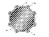
20 절연성 입자
30, 31, 32, 33, 34 도전층
40 도전성 입자
41 수지 코어 입자
42 절연성 입자
50 제 1 회로 부재
51 단자
52 산화물층
Claims (8)
- 수지 코어 입자와, 상기 수지 코어 입자의 표면에 복수 배치되어, 돌기를 형성하는 절연성 입자와, 상기 수지 코어 입자 및 상기 절연성 입자의 표면에 배치되는 도전층을 구비하고, 상기 절연성 입자의 모스 경도가 7 보다 큰 도전성 입자를 함유하는 도전 재료.
- 제 1 항에 있어서,
상기 도전성 입자의 도전층이 니켈 또는 니켈 합금인 도전 재료. - 제 1 항 또는 제 2 항에 있어서,
상기 도전성 입자의 절연성 입자가, 지르코니아, 알루미나, 탄화텅스텐, 및 다이아몬드 내 중 적어도 1 종 이상인 도전 재료. - 제 1 항 내지 제 3 항 중 어느 한 항에 있어서,
상기 도전성 입자의 절연성 입자의 평균 입자경이 50 ∼ 250 ㎚ 이고,
상기 도전성 입자의 수지 코어 입자의 표면에 형성된 돌기의 개수가 1 ∼ 500 인 도전 재료. - 제 1 항 내지 제 4 항 중 어느 한 항에 있어서,
상기 도전성 입자의 수지 코어 입자의 20 % 압축되었을 때의 압축 탄성률이 500 ∼ 20000 N/㎟ 인 도전 재료. - 제 1 항 내지 제 5 항 중 어느 한 항에 있어서,
플라스틱 기판 상의 산화물층이 형성된 단자를 접속하는 도전 재료. - 수지 코어 입자와, 상기 수지 코어 입자의 표면에 복수 배치되어, 돌기를 형성하는 절연성 입자와, 상기 수지 코어 입자 및 상기 절연성 입자의 표면에 배치되는 도전층을 구비하고, 상기 절연성 입자의 모스 경도가 7 보다 큰 도전성 입자에 의해 제 1 회로 부재의 단자와 제 2 회로 부재의 단자가 접속되어 이루어지는 접속 구조체.
- 수지 코어 입자와, 상기 수지 코어 입자의 표면에 복수 배치되어, 돌기를 형성하는 절연성 입자와, 상기 수지 코어 입자 및 상기 절연성 입자의 표면에 배치되는 도전층을 구비하고, 상기 절연성 입자의 모스 경도가 7 보다 큰 도전성 입자를 함유하는 도전 재료를 개재하여, 제 1 회로 부재의 단자와 제 2 회로 부재의 단자를 압착하는 접속 구조체의 제조 방법.
Applications Claiming Priority (5)
| Application Number | Priority Date | Filing Date | Title |
|---|---|---|---|
| JP2014220448 | 2014-10-29 | ||
| JPJP-P-2014-220448 | 2014-10-29 | ||
| JP2015201767A JP2016089153A (ja) | 2014-10-29 | 2015-10-13 | 導電材料 |
| JPJP-P-2015-201767 | 2015-10-13 | ||
| PCT/JP2015/080327 WO2016068165A1 (ja) | 2014-10-29 | 2015-10-28 | 導電材料 |
Related Child Applications (1)
| Application Number | Title | Priority Date | Filing Date |
|---|---|---|---|
| KR1020197002161A Division KR20190009852A (ko) | 2014-10-29 | 2015-10-28 | 도전 재료 |
Publications (1)
| Publication Number | Publication Date |
|---|---|
| KR20170036721A true KR20170036721A (ko) | 2017-04-03 |
Family
ID=56015903
Family Applications (2)
| Application Number | Title | Priority Date | Filing Date |
|---|---|---|---|
| KR1020177004503A Ceased KR20170036721A (ko) | 2014-10-29 | 2015-10-28 | 도전 재료 |
| KR1020197002161A Ceased KR20190009852A (ko) | 2014-10-29 | 2015-10-28 | 도전 재료 |
Family Applications After (1)
| Application Number | Title | Priority Date | Filing Date |
|---|---|---|---|
| KR1020197002161A Ceased KR20190009852A (ko) | 2014-10-29 | 2015-10-28 | 도전 재료 |
Country Status (4)
| Country | Link |
|---|---|
| US (1) | US10177465B2 (ko) |
| JP (3) | JP2016089153A (ko) |
| KR (2) | KR20170036721A (ko) |
| CN (1) | CN106796826A (ko) |
Families Citing this family (10)
| Publication number | Priority date | Publication date | Assignee | Title |
|---|---|---|---|---|
| CN109564240A (zh) * | 2016-08-08 | 2019-04-02 | 积水化学工业株式会社 | 导通检测装置用部件和导通检测装置 |
| JP7039883B2 (ja) | 2016-12-01 | 2022-03-23 | デクセリアルズ株式会社 | 異方性導電フィルム |
| JP7284554B2 (ja) * | 2016-12-06 | 2023-05-31 | 積水化学工業株式会社 | 粒子材料、導電性粒子、導電材料、接続材料及び接続構造体 |
| US10964441B2 (en) * | 2016-12-21 | 2021-03-30 | 3M Innovative Properties Company | Conductive particles, articles, and methods |
| CN110546222A (zh) * | 2017-04-28 | 2019-12-06 | 日立化成株式会社 | 粘接剂组合物及连接体的制造方法 |
| KR102180143B1 (ko) * | 2017-12-29 | 2020-11-17 | 국도화학 주식회사 | 이방 도전성 필름, 이를 포함하는 디스플레이 장치 및/또는 이를 포함하는 반도체 장치 |
| CN111902884B (zh) * | 2018-04-04 | 2023-03-14 | 积水化学工业株式会社 | 导电性粒子、其制造方法、导电材料及连接结构体 |
| CN111971757B (zh) * | 2018-04-04 | 2023-03-14 | 积水化学工业株式会社 | 导电性粒子、其制造方法、导电材料及连接结构体 |
| CN113012566A (zh) * | 2019-12-19 | 2021-06-22 | 群创光电股份有限公司 | 可挠性显示装置以及其制作方法 |
| KR20230134656A (ko) * | 2022-03-14 | 2023-09-22 | 삼성디스플레이 주식회사 | 이방성 도전 필름 및 이를 포함하는 표시 장치 |
Citations (5)
| Publication number | Priority date | Publication date | Assignee | Title |
|---|---|---|---|---|
| KR20080072658A (ko) * | 2005-11-18 | 2008-08-06 | 히다치 가세고교 가부시끼가이샤 | 접착제 조성물, 회로 접속 재료, 접속 구조 및 회로부재의접속방법 |
| KR20130016387A (ko) * | 2010-07-02 | 2013-02-14 | 세키스이가가쿠 고교가부시키가이샤 | 절연성 입자 부착 도전성 입자, 이방성 도전 재료 및 접속 구조체 |
| JP2013149613A (ja) | 2011-12-22 | 2013-08-01 | Sekisui Chem Co Ltd | 導電性粒子、導電材料及び接続構造体 |
| JP2013149611A (ja) * | 2011-12-22 | 2013-08-01 | Sekisui Chem Co Ltd | 導電性粒子、導電材料及び接続構造体 |
| KR20140106384A (ko) * | 2011-12-21 | 2014-09-03 | 세키스이가가쿠 고교가부시키가이샤 | 도전성 입자, 도전 재료 및 접속 구조체 |
Family Cites Families (13)
| Publication number | Priority date | Publication date | Assignee | Title |
|---|---|---|---|---|
| US4740657A (en) * | 1986-02-14 | 1988-04-26 | Hitachi, Chemical Company, Ltd | Anisotropic-electroconductive adhesive composition, method for connecting circuits using the same, and connected circuit structure thus obtained |
| JPS62206772A (ja) | 1986-03-06 | 1987-09-11 | 日立化成工業株式会社 | 回路の接続構造体 |
| FR2625863B1 (fr) * | 1988-01-13 | 1992-01-24 | Caplatex Sa | Procede de fabrication d'un joint de blindage electromagnetique, machine pour l'execution de ce procede, et joint obtenu a l'aide de ce procede ou de cette machine |
| US4857668A (en) * | 1988-04-15 | 1989-08-15 | Schlegel Corporation | Multi-function gasket |
| JP2510404Y2 (ja) * | 1990-11-29 | 1996-09-11 | 北川工業株式会社 | 電磁波シ―ルド用ガスケット |
| WO1997008928A1 (en) * | 1995-08-25 | 1997-03-06 | Parker-Hannifin Corporation | Emi shielding gasket having a consolidated conductive sheathing |
| JP3541777B2 (ja) * | 2000-03-15 | 2004-07-14 | ソニーケミカル株式会社 | 異方性導電接続材料 |
| KR101131229B1 (ko) * | 2004-01-30 | 2012-03-28 | 세키스이가가쿠 고교가부시키가이샤 | 도전성 미립자 및 이방성 도전 재료 |
| JP5430093B2 (ja) * | 2008-07-24 | 2014-02-26 | デクセリアルズ株式会社 | 導電性粒子、異方性導電フィルム、及び接合体、並びに、接続方法 |
| KR101271814B1 (ko) * | 2009-07-02 | 2013-06-07 | 히타치가세이가부시끼가이샤 | 도전 입자 |
| JP5768454B2 (ja) * | 2011-04-14 | 2015-08-26 | デクセリアルズ株式会社 | 異方性導電フィルム |
| JP2013105636A (ja) * | 2011-11-14 | 2013-05-30 | Dexerials Corp | 異方性導電フィルム、接続方法、及び接合体 |
| JP6212366B2 (ja) * | 2013-08-09 | 2017-10-11 | 積水化学工業株式会社 | 導電性粒子、導電材料及び接続構造体 |
-
2015
- 2015-10-13 JP JP2015201767A patent/JP2016089153A/ja active Pending
- 2015-10-28 KR KR1020177004503A patent/KR20170036721A/ko not_active Ceased
- 2015-10-28 US US15/523,592 patent/US10177465B2/en active Active
- 2015-10-28 CN CN201580055242.3A patent/CN106796826A/zh active Pending
- 2015-10-28 KR KR1020197002161A patent/KR20190009852A/ko not_active Ceased
-
2020
- 2020-06-10 JP JP2020100864A patent/JP7100088B2/ja active Active
-
2022
- 2022-06-30 JP JP2022105740A patent/JP7506714B2/ja active Active
Patent Citations (5)
| Publication number | Priority date | Publication date | Assignee | Title |
|---|---|---|---|---|
| KR20080072658A (ko) * | 2005-11-18 | 2008-08-06 | 히다치 가세고교 가부시끼가이샤 | 접착제 조성물, 회로 접속 재료, 접속 구조 및 회로부재의접속방법 |
| KR20130016387A (ko) * | 2010-07-02 | 2013-02-14 | 세키스이가가쿠 고교가부시키가이샤 | 절연성 입자 부착 도전성 입자, 이방성 도전 재료 및 접속 구조체 |
| KR20140106384A (ko) * | 2011-12-21 | 2014-09-03 | 세키스이가가쿠 고교가부시키가이샤 | 도전성 입자, 도전 재료 및 접속 구조체 |
| JP2013149613A (ja) | 2011-12-22 | 2013-08-01 | Sekisui Chem Co Ltd | 導電性粒子、導電材料及び接続構造体 |
| JP2013149611A (ja) * | 2011-12-22 | 2013-08-01 | Sekisui Chem Co Ltd | 導電性粒子、導電材料及び接続構造体 |
Also Published As
| Publication number | Publication date |
|---|---|
| US10177465B2 (en) | 2019-01-08 |
| JP7506714B2 (ja) | 2024-06-26 |
| CN106796826A (zh) | 2017-05-31 |
| US20170310020A1 (en) | 2017-10-26 |
| JP2022132316A (ja) | 2022-09-08 |
| JP2016089153A (ja) | 2016-05-23 |
| JP2020170706A (ja) | 2020-10-15 |
| JP7100088B2 (ja) | 2022-07-12 |
| KR20190009852A (ko) | 2019-01-29 |
Similar Documents
| Publication | Publication Date | Title |
|---|---|---|
| JP7100088B2 (ja) | 導電材料 | |
| KR102517498B1 (ko) | 도전 재료, 및 접속체의 제조 방법 | |
| JP6212366B2 (ja) | 導電性粒子、導電材料及び接続構造体 | |
| TW201832415A (zh) | 異向性導電膜、連接結構體、連接結構體之製造方法及連接方法 | |
| KR20190133023A (ko) | 도전 입자의 선별 방법, 회로 접속 재료, 접속 구조체 및 그의 제조 방법, 그리고 도전 입자 | |
| CN102408840A (zh) | 粘接膜、以及电路部件的连接结构和连接方法 | |
| KR102707315B1 (ko) | 접속 재료 | |
| JP2013004202A (ja) | 異方性導電材料及び接続構造体 | |
| KR102545861B1 (ko) | 도전 재료 | |
| KR20110136731A (ko) | 회로 접속용 접착 필름 및 그의 용도, 회로 접속 구조체 및 그의 제조 방법 및 회로 부재의 접속 방법 | |
| HK40045320B (en) | Method for preparing connection structure, connection structure and conductive material | |
| HK40045320A (en) | Method for preparing connection structure, connection structure and conductive material | |
| JP7193512B2 (ja) | 接続材料 | |
| HK40051347A (en) | Connection material | |
| HK1238409A1 (en) | Conductive material | |
| KR20110136732A (ko) | 회로 접속용 접착 필름 및 그의 용도, 회로 접속 구조체 및 그의 제조 방법 및 회로 부재의 접속 방법 |
Legal Events
| Date | Code | Title | Description |
|---|---|---|---|
| A201 | Request for examination | ||
| PA0105 | International application |
Patent event date: 20170217 Patent event code: PA01051R01D Comment text: International Patent Application |
|
| PA0201 | Request for examination | ||
| PG1501 | Laying open of application | ||
| E902 | Notification of reason for refusal | ||
| PE0902 | Notice of grounds for rejection |
Comment text: Notification of reason for refusal Patent event date: 20180426 Patent event code: PE09021S01D |
|
| AMND | Amendment | ||
| E601 | Decision to refuse application | ||
| PE0601 | Decision on rejection of patent |
Patent event date: 20181029 Comment text: Decision to Refuse Application Patent event code: PE06012S01D Patent event date: 20180426 Comment text: Notification of reason for refusal Patent event code: PE06011S01I |
|
| X091 | Application refused [patent] | ||
| AMND | Amendment | ||
| PX0901 | Re-examination |
Patent event code: PX09011S01I Patent event date: 20181029 Comment text: Decision to Refuse Application Patent event code: PX09012R01I Patent event date: 20180626 Comment text: Amendment to Specification, etc. |
|
| PX0601 | Decision of rejection after re-examination |
Comment text: Decision to Refuse Application Patent event code: PX06014S01D Patent event date: 20181221 Comment text: Amendment to Specification, etc. Patent event code: PX06012R01I Patent event date: 20181126 Comment text: Decision to Refuse Application Patent event code: PX06011S01I Patent event date: 20181029 Comment text: Amendment to Specification, etc. Patent event code: PX06012R01I Patent event date: 20180626 Comment text: Notification of reason for refusal Patent event code: PX06013S01I Patent event date: 20180426 |
|
| A107 | Divisional application of patent | ||
| J201 | Request for trial against refusal decision | ||
| PA0104 | Divisional application for international application |
Comment text: Divisional Application for International Patent Patent event code: PA01041R01D Patent event date: 20190122 |
|
| PJ0201 | Trial against decision of rejection |
Patent event date: 20190122 Comment text: Request for Trial against Decision on Refusal Patent event code: PJ02012R01D Patent event date: 20181221 Comment text: Decision to Refuse Application Patent event code: PJ02011S01I Patent event date: 20181029 Comment text: Decision to Refuse Application Patent event code: PJ02011S01I Appeal kind category: Appeal against decision to decline refusal Appeal identifier: 2019101000233 Request date: 20190122 |
|
| J301 | Trial decision |
Free format text: TRIAL NUMBER: 2019101000233; TRIAL DECISION FOR APPEAL AGAINST DECISION TO DECLINE REFUSAL REQUESTED 20190122 Effective date: 20200130 |
|
| PJ1301 | Trial decision |
Patent event code: PJ13011S01D Patent event date: 20200130 Comment text: Trial Decision on Objection to Decision on Refusal Appeal kind category: Appeal against decision to decline refusal Request date: 20190122 Decision date: 20200130 Appeal identifier: 2019101000233 |
|
| J121 | Written withdrawal of request for trial | ||
| PC1202 | Submission of document of withdrawal before decision of registration |
Comment text: [Withdrawal of Procedure relating to Patent, etc.] Withdrawal (Abandonment) Patent event code: PC12021R01D Patent event date: 20200210 |
|
| PJ1201 | Withdrawal of trial |
Patent event code: PJ12011R01D Patent event date: 20200210 Comment text: Written Withdrawal of Request for Trial Appeal identifier: 2019101000233 Request date: 20190122 Appeal kind category: Appeal against decision to decline refusal Decision date: 20200130 |
|
| WITB | Written withdrawal of application |