KR20170036742A - 도전 필름 적층체, 도전체 및 도전체의 제조 방법 - Google Patents
도전 필름 적층체, 도전체 및 도전체의 제조 방법 Download PDFInfo
- Publication number
- KR20170036742A KR20170036742A KR1020177005031A KR20177005031A KR20170036742A KR 20170036742 A KR20170036742 A KR 20170036742A KR 1020177005031 A KR1020177005031 A KR 1020177005031A KR 20177005031 A KR20177005031 A KR 20177005031A KR 20170036742 A KR20170036742 A KR 20170036742A
- Authority
- KR
- South Korea
- Prior art keywords
- conductive film
- film laminate
- touch panel
- openings
- forming
- Prior art date
- Legal status (The legal status is an assumption and is not a legal conclusion. Google has not performed a legal analysis and makes no representation as to the accuracy of the status listed.)
- Granted
Links
Images







Classifications
-
- B—PERFORMING OPERATIONS; TRANSPORTING
- B32—LAYERED PRODUCTS
- B32B—LAYERED PRODUCTS, i.e. PRODUCTS BUILT-UP OF STRATA OF FLAT OR NON-FLAT, e.g. CELLULAR OR HONEYCOMB, FORM
- B32B7/00—Layered products characterised by the relation between layers; Layered products characterised by the relative orientation of features between layers, or by the relative values of a measurable parameter between layers, i.e. products comprising layers having different physical, chemical or physicochemical properties; Layered products characterised by the interconnection of layers
- B32B7/02—Physical, chemical or physicochemical properties
-
- B—PERFORMING OPERATIONS; TRANSPORTING
- B32—LAYERED PRODUCTS
- B32B—LAYERED PRODUCTS, i.e. PRODUCTS BUILT-UP OF STRATA OF FLAT OR NON-FLAT, e.g. CELLULAR OR HONEYCOMB, FORM
- B32B3/00—Layered products comprising a layer with external or internal discontinuities or unevennesses, or a layer of non-planar shape; Layered products comprising a layer having particular features of form
- B32B3/26—Layered products comprising a layer with external or internal discontinuities or unevennesses, or a layer of non-planar shape; Layered products comprising a layer having particular features of form characterised by a particular shape of the outline of the cross-section of a continuous layer; characterised by a layer with cavities or internal voids ; characterised by an apertured layer
- B32B3/266—Layered products comprising a layer with external or internal discontinuities or unevennesses, or a layer of non-planar shape; Layered products comprising a layer having particular features of form characterised by a particular shape of the outline of the cross-section of a continuous layer; characterised by a layer with cavities or internal voids ; characterised by an apertured layer characterised by an apertured layer, the apertures going through the whole thickness of the layer, e.g. expanded metal, perforated layer, slit layer regular cells B32B3/12
-
- B—PERFORMING OPERATIONS; TRANSPORTING
- B21—MECHANICAL METAL-WORKING WITHOUT ESSENTIALLY REMOVING MATERIAL; PUNCHING METAL
- B21D—WORKING OR PROCESSING OF SHEET METAL OR METAL TUBES, RODS OR PROFILES WITHOUT ESSENTIALLY REMOVING MATERIAL; PUNCHING METAL
- B21D22/00—Shaping without cutting, by stamping, spinning, or deep-drawing
- B21D22/20—Deep-drawing
- B21D22/203—Deep-drawing of compound articles
-
- B—PERFORMING OPERATIONS; TRANSPORTING
- B21—MECHANICAL METAL-WORKING WITHOUT ESSENTIALLY REMOVING MATERIAL; PUNCHING METAL
- B21D—WORKING OR PROCESSING OF SHEET METAL OR METAL TUBES, RODS OR PROFILES WITHOUT ESSENTIALLY REMOVING MATERIAL; PUNCHING METAL
- B21D24/00—Special deep-drawing arrangements in, or in connection with, presses
- B21D24/16—Additional equipment in association with the tools, e.g. for shearing, for trimming
-
- B—PERFORMING OPERATIONS; TRANSPORTING
- B29—WORKING OF PLASTICS; WORKING OF SUBSTANCES IN A PLASTIC STATE IN GENERAL
- B29C—SHAPING OR JOINING OF PLASTICS; SHAPING OF MATERIAL IN A PLASTIC STATE, NOT OTHERWISE PROVIDED FOR; AFTER-TREATMENT OF THE SHAPED PRODUCTS, e.g. REPAIRING
- B29C51/00—Shaping by thermoforming, i.e. shaping sheets or sheet like preforms after heating, e.g. shaping sheets in matched moulds or by deep-drawing; Apparatus therefor
-
- B—PERFORMING OPERATIONS; TRANSPORTING
- B32—LAYERED PRODUCTS
- B32B—LAYERED PRODUCTS, i.e. PRODUCTS BUILT-UP OF STRATA OF FLAT OR NON-FLAT, e.g. CELLULAR OR HONEYCOMB, FORM
- B32B1/00—Layered products having a non-planar shape
- B32B1/08—Tubular products
-
- B—PERFORMING OPERATIONS; TRANSPORTING
- B32—LAYERED PRODUCTS
- B32B—LAYERED PRODUCTS, i.e. PRODUCTS BUILT-UP OF STRATA OF FLAT OR NON-FLAT, e.g. CELLULAR OR HONEYCOMB, FORM
- B32B27/00—Layered products comprising a layer of synthetic resin
- B32B27/06—Layered products comprising a layer of synthetic resin as the main or only constituent of a layer, which is next to another layer of the same or of a different material
- B32B27/08—Layered products comprising a layer of synthetic resin as the main or only constituent of a layer, which is next to another layer of the same or of a different material of synthetic resin
-
- B—PERFORMING OPERATIONS; TRANSPORTING
- B32—LAYERED PRODUCTS
- B32B—LAYERED PRODUCTS, i.e. PRODUCTS BUILT-UP OF STRATA OF FLAT OR NON-FLAT, e.g. CELLULAR OR HONEYCOMB, FORM
- B32B27/00—Layered products comprising a layer of synthetic resin
- B32B27/16—Layered products comprising a layer of synthetic resin specially treated, e.g. irradiated
-
- B—PERFORMING OPERATIONS; TRANSPORTING
- B32—LAYERED PRODUCTS
- B32B—LAYERED PRODUCTS, i.e. PRODUCTS BUILT-UP OF STRATA OF FLAT OR NON-FLAT, e.g. CELLULAR OR HONEYCOMB, FORM
- B32B27/00—Layered products comprising a layer of synthetic resin
- B32B27/30—Layered products comprising a layer of synthetic resin comprising vinyl (co)polymers; comprising acrylic (co)polymers
- B32B27/308—Layered products comprising a layer of synthetic resin comprising vinyl (co)polymers; comprising acrylic (co)polymers comprising acrylic (co)polymers
-
- B—PERFORMING OPERATIONS; TRANSPORTING
- B32—LAYERED PRODUCTS
- B32B—LAYERED PRODUCTS, i.e. PRODUCTS BUILT-UP OF STRATA OF FLAT OR NON-FLAT, e.g. CELLULAR OR HONEYCOMB, FORM
- B32B27/00—Layered products comprising a layer of synthetic resin
- B32B27/32—Layered products comprising a layer of synthetic resin comprising polyolefins
- B32B27/325—Layered products comprising a layer of synthetic resin comprising polyolefins comprising polycycloolefins
-
- B—PERFORMING OPERATIONS; TRANSPORTING
- B32—LAYERED PRODUCTS
- B32B—LAYERED PRODUCTS, i.e. PRODUCTS BUILT-UP OF STRATA OF FLAT OR NON-FLAT, e.g. CELLULAR OR HONEYCOMB, FORM
- B32B27/00—Layered products comprising a layer of synthetic resin
- B32B27/36—Layered products comprising a layer of synthetic resin comprising polyesters
-
- B—PERFORMING OPERATIONS; TRANSPORTING
- B32—LAYERED PRODUCTS
- B32B—LAYERED PRODUCTS, i.e. PRODUCTS BUILT-UP OF STRATA OF FLAT OR NON-FLAT, e.g. CELLULAR OR HONEYCOMB, FORM
- B32B27/00—Layered products comprising a layer of synthetic resin
- B32B27/36—Layered products comprising a layer of synthetic resin comprising polyesters
- B32B27/365—Layered products comprising a layer of synthetic resin comprising polyesters comprising polycarbonates
-
- B—PERFORMING OPERATIONS; TRANSPORTING
- B32—LAYERED PRODUCTS
- B32B—LAYERED PRODUCTS, i.e. PRODUCTS BUILT-UP OF STRATA OF FLAT OR NON-FLAT, e.g. CELLULAR OR HONEYCOMB, FORM
- B32B3/00—Layered products comprising a layer with external or internal discontinuities or unevennesses, or a layer of non-planar shape; Layered products comprising a layer having particular features of form
- B32B3/02—Layered products comprising a layer with external or internal discontinuities or unevennesses, or a layer of non-planar shape; Layered products comprising a layer having particular features of form characterised by features of form at particular places, e.g. in edge regions
-
- B—PERFORMING OPERATIONS; TRANSPORTING
- B32—LAYERED PRODUCTS
- B32B—LAYERED PRODUCTS, i.e. PRODUCTS BUILT-UP OF STRATA OF FLAT OR NON-FLAT, e.g. CELLULAR OR HONEYCOMB, FORM
- B32B37/00—Methods or apparatus for laminating, e.g. by curing or by ultrasonic bonding
- B32B37/10—Methods or apparatus for laminating, e.g. by curing or by ultrasonic bonding characterised by the pressing technique, e.g. using action of vacuum or fluid pressure
-
- B—PERFORMING OPERATIONS; TRANSPORTING
- B32—LAYERED PRODUCTS
- B32B—LAYERED PRODUCTS, i.e. PRODUCTS BUILT-UP OF STRATA OF FLAT OR NON-FLAT, e.g. CELLULAR OR HONEYCOMB, FORM
- B32B37/00—Methods or apparatus for laminating, e.g. by curing or by ultrasonic bonding
- B32B37/14—Methods or apparatus for laminating, e.g. by curing or by ultrasonic bonding characterised by the properties of the layers
-
- B—PERFORMING OPERATIONS; TRANSPORTING
- B32—LAYERED PRODUCTS
- B32B—LAYERED PRODUCTS, i.e. PRODUCTS BUILT-UP OF STRATA OF FLAT OR NON-FLAT, e.g. CELLULAR OR HONEYCOMB, FORM
- B32B7/00—Layered products characterised by the relation between layers; Layered products characterised by the relative orientation of features between layers, or by the relative values of a measurable parameter between layers, i.e. products comprising layers having different physical, chemical or physicochemical properties; Layered products characterised by the interconnection of layers
- B32B7/02—Physical, chemical or physicochemical properties
- B32B7/025—Electric or magnetic properties
-
- B—PERFORMING OPERATIONS; TRANSPORTING
- B32—LAYERED PRODUCTS
- B32B—LAYERED PRODUCTS, i.e. PRODUCTS BUILT-UP OF STRATA OF FLAT OR NON-FLAT, e.g. CELLULAR OR HONEYCOMB, FORM
- B32B7/00—Layered products characterised by the relation between layers; Layered products characterised by the relative orientation of features between layers, or by the relative values of a measurable parameter between layers, i.e. products comprising layers having different physical, chemical or physicochemical properties; Layered products characterised by the interconnection of layers
- B32B7/04—Interconnection of layers
- B32B7/12—Interconnection of layers using interposed adhesives or interposed materials with bonding properties
-
- G—PHYSICS
- G02—OPTICS
- G02F—OPTICAL DEVICES OR ARRANGEMENTS FOR THE CONTROL OF LIGHT BY MODIFICATION OF THE OPTICAL PROPERTIES OF THE MEDIA OF THE ELEMENTS INVOLVED THEREIN; NON-LINEAR OPTICS; FREQUENCY-CHANGING OF LIGHT; OPTICAL LOGIC ELEMENTS; OPTICAL ANALOGUE/DIGITAL CONVERTERS
- G02F1/00—Devices or arrangements for the control of the intensity, colour, phase, polarisation or direction of light arriving from an independent light source, e.g. switching, gating or modulating; Non-linear optics
- G02F1/01—Devices or arrangements for the control of the intensity, colour, phase, polarisation or direction of light arriving from an independent light source, e.g. switching, gating or modulating; Non-linear optics for the control of the intensity, phase, polarisation or colour
- G02F1/13—Devices or arrangements for the control of the intensity, colour, phase, polarisation or direction of light arriving from an independent light source, e.g. switching, gating or modulating; Non-linear optics for the control of the intensity, phase, polarisation or colour based on liquid crystals, e.g. single liquid crystal display cells
- G02F1/133—Constructional arrangements; Operation of liquid crystal cells; Circuit arrangements
- G02F1/1333—Constructional arrangements; Manufacturing methods
- G02F1/13338—Input devices, e.g. touch panels
-
- G—PHYSICS
- G06—COMPUTING OR CALCULATING; COUNTING
- G06F—ELECTRIC DIGITAL DATA PROCESSING
- G06F3/00—Input arrangements for transferring data to be processed into a form capable of being handled by the computer; Output arrangements for transferring data from processing unit to output unit, e.g. interface arrangements
- G06F3/01—Input arrangements or combined input and output arrangements for interaction between user and computer
- G06F3/03—Arrangements for converting the position or the displacement of a member into a coded form
- G06F3/041—Digitisers, e.g. for touch screens or touch pads, characterised by the transducing means
-
- G—PHYSICS
- G06—COMPUTING OR CALCULATING; COUNTING
- G06F—ELECTRIC DIGITAL DATA PROCESSING
- G06F3/00—Input arrangements for transferring data to be processed into a form capable of being handled by the computer; Output arrangements for transferring data from processing unit to output unit, e.g. interface arrangements
- G06F3/01—Input arrangements or combined input and output arrangements for interaction between user and computer
- G06F3/03—Arrangements for converting the position or the displacement of a member into a coded form
- G06F3/041—Digitisers, e.g. for touch screens or touch pads, characterised by the transducing means
- G06F3/044—Digitisers, e.g. for touch screens or touch pads, characterised by the transducing means by capacitive means
-
- H—ELECTRICITY
- H01—ELECTRIC ELEMENTS
- H01B—CABLES; CONDUCTORS; INSULATORS; SELECTION OF MATERIALS FOR THEIR CONDUCTIVE, INSULATING OR DIELECTRIC PROPERTIES
- H01B5/00—Non-insulated conductors or conductive bodies characterised by their form
- H01B5/14—Non-insulated conductors or conductive bodies characterised by their form comprising conductive layers or films on insulating-supports
-
- B—PERFORMING OPERATIONS; TRANSPORTING
- B29—WORKING OF PLASTICS; WORKING OF SUBSTANCES IN A PLASTIC STATE IN GENERAL
- B29C—SHAPING OR JOINING OF PLASTICS; SHAPING OF MATERIAL IN A PLASTIC STATE, NOT OTHERWISE PROVIDED FOR; AFTER-TREATMENT OF THE SHAPED PRODUCTS, e.g. REPAIRING
- B29C51/00—Shaping by thermoforming, i.e. shaping sheets or sheet like preforms after heating, e.g. shaping sheets in matched moulds or by deep-drawing; Apparatus therefor
- B29C51/08—Deep drawing or matched-mould forming, i.e. using mechanical means only
-
- B—PERFORMING OPERATIONS; TRANSPORTING
- B29—WORKING OF PLASTICS; WORKING OF SUBSTANCES IN A PLASTIC STATE IN GENERAL
- B29C—SHAPING OR JOINING OF PLASTICS; SHAPING OF MATERIAL IN A PLASTIC STATE, NOT OTHERWISE PROVIDED FOR; AFTER-TREATMENT OF THE SHAPED PRODUCTS, e.g. REPAIRING
- B29C51/00—Shaping by thermoforming, i.e. shaping sheets or sheet like preforms after heating, e.g. shaping sheets in matched moulds or by deep-drawing; Apparatus therefor
- B29C51/14—Shaping by thermoforming, i.e. shaping sheets or sheet like preforms after heating, e.g. shaping sheets in matched moulds or by deep-drawing; Apparatus therefor using multilayered preforms or sheets
-
- B—PERFORMING OPERATIONS; TRANSPORTING
- B29—WORKING OF PLASTICS; WORKING OF SUBSTANCES IN A PLASTIC STATE IN GENERAL
- B29K—INDEXING SCHEME ASSOCIATED WITH SUBCLASSES B29B, B29C OR B29D, RELATING TO MOULDING MATERIALS OR TO MATERIALS FOR MOULDS, REINFORCEMENTS, FILLERS OR PREFORMED PARTS, e.g. INSERTS
- B29K2105/00—Condition, form or state of moulded material or of the material to be shaped
- B29K2105/0005—Condition, form or state of moulded material or of the material to be shaped containing compounding ingredients
- B29K2105/002—Agents changing electric characteristics
- B29K2105/0023—Agents changing electric characteristics improving electric conduction
-
- B—PERFORMING OPERATIONS; TRANSPORTING
- B29—WORKING OF PLASTICS; WORKING OF SUBSTANCES IN A PLASTIC STATE IN GENERAL
- B29K—INDEXING SCHEME ASSOCIATED WITH SUBCLASSES B29B, B29C OR B29D, RELATING TO MOULDING MATERIALS OR TO MATERIALS FOR MOULDS, REINFORCEMENTS, FILLERS OR PREFORMED PARTS, e.g. INSERTS
- B29K2995/00—Properties of moulding materials, reinforcements, fillers, preformed parts or moulds
- B29K2995/0003—Properties of moulding materials, reinforcements, fillers, preformed parts or moulds having particular electrical or magnetic properties, e.g. piezoelectric
- B29K2995/0005—Conductive
-
- B—PERFORMING OPERATIONS; TRANSPORTING
- B32—LAYERED PRODUCTS
- B32B—LAYERED PRODUCTS, i.e. PRODUCTS BUILT-UP OF STRATA OF FLAT OR NON-FLAT, e.g. CELLULAR OR HONEYCOMB, FORM
- B32B2250/00—Layers arrangement
- B32B2250/02—2 layers
-
- B—PERFORMING OPERATIONS; TRANSPORTING
- B32—LAYERED PRODUCTS
- B32B—LAYERED PRODUCTS, i.e. PRODUCTS BUILT-UP OF STRATA OF FLAT OR NON-FLAT, e.g. CELLULAR OR HONEYCOMB, FORM
- B32B2255/00—Coating on the layer surface
- B32B2255/10—Coating on the layer surface on synthetic resin layer or on natural or synthetic rubber layer
-
- B—PERFORMING OPERATIONS; TRANSPORTING
- B32—LAYERED PRODUCTS
- B32B—LAYERED PRODUCTS, i.e. PRODUCTS BUILT-UP OF STRATA OF FLAT OR NON-FLAT, e.g. CELLULAR OR HONEYCOMB, FORM
- B32B2255/00—Coating on the layer surface
- B32B2255/20—Inorganic coating
-
- B—PERFORMING OPERATIONS; TRANSPORTING
- B32—LAYERED PRODUCTS
- B32B—LAYERED PRODUCTS, i.e. PRODUCTS BUILT-UP OF STRATA OF FLAT OR NON-FLAT, e.g. CELLULAR OR HONEYCOMB, FORM
- B32B2307/00—Properties of the layers or laminate
- B32B2307/20—Properties of the layers or laminate having particular electrical or magnetic properties, e.g. piezoelectric
- B32B2307/202—Conductive
-
- B—PERFORMING OPERATIONS; TRANSPORTING
- B32—LAYERED PRODUCTS
- B32B—LAYERED PRODUCTS, i.e. PRODUCTS BUILT-UP OF STRATA OF FLAT OR NON-FLAT, e.g. CELLULAR OR HONEYCOMB, FORM
- B32B2307/00—Properties of the layers or laminate
- B32B2307/20—Properties of the layers or laminate having particular electrical or magnetic properties, e.g. piezoelectric
- B32B2307/206—Insulating
-
- B—PERFORMING OPERATIONS; TRANSPORTING
- B32—LAYERED PRODUCTS
- B32B—LAYERED PRODUCTS, i.e. PRODUCTS BUILT-UP OF STRATA OF FLAT OR NON-FLAT, e.g. CELLULAR OR HONEYCOMB, FORM
- B32B2307/00—Properties of the layers or laminate
- B32B2307/40—Properties of the layers or laminate having particular optical properties
- B32B2307/412—Transparent
-
- B—PERFORMING OPERATIONS; TRANSPORTING
- B32—LAYERED PRODUCTS
- B32B—LAYERED PRODUCTS, i.e. PRODUCTS BUILT-UP OF STRATA OF FLAT OR NON-FLAT, e.g. CELLULAR OR HONEYCOMB, FORM
- B32B2307/00—Properties of the layers or laminate
- B32B2307/50—Properties of the layers or laminate having particular mechanical properties
-
- B—PERFORMING OPERATIONS; TRANSPORTING
- B32—LAYERED PRODUCTS
- B32B—LAYERED PRODUCTS, i.e. PRODUCTS BUILT-UP OF STRATA OF FLAT OR NON-FLAT, e.g. CELLULAR OR HONEYCOMB, FORM
- B32B2307/00—Properties of the layers or laminate
- B32B2307/50—Properties of the layers or laminate having particular mechanical properties
- B32B2307/514—Oriented
- B32B2307/518—Oriented bi-axially
-
- B—PERFORMING OPERATIONS; TRANSPORTING
- B32—LAYERED PRODUCTS
- B32B—LAYERED PRODUCTS, i.e. PRODUCTS BUILT-UP OF STRATA OF FLAT OR NON-FLAT, e.g. CELLULAR OR HONEYCOMB, FORM
- B32B2307/00—Properties of the layers or laminate
- B32B2307/70—Other properties
- B32B2307/732—Dimensional properties
-
- B—PERFORMING OPERATIONS; TRANSPORTING
- B32—LAYERED PRODUCTS
- B32B—LAYERED PRODUCTS, i.e. PRODUCTS BUILT-UP OF STRATA OF FLAT OR NON-FLAT, e.g. CELLULAR OR HONEYCOMB, FORM
- B32B2457/00—Electrical equipment
- B32B2457/20—Displays, e.g. liquid crystal displays, plasma displays
- B32B2457/208—Touch screens
-
- G—PHYSICS
- G06—COMPUTING OR CALCULATING; COUNTING
- G06F—ELECTRIC DIGITAL DATA PROCESSING
- G06F2203/00—Indexing scheme relating to G06F3/00 - G06F3/048
- G06F2203/041—Indexing scheme relating to G06F3/041 - G06F3/045
- G06F2203/04102—Flexible digitiser, i.e. constructional details for allowing the whole digitising part of a device to be flexed or rolled like a sheet of paper
-
- G—PHYSICS
- G06—COMPUTING OR CALCULATING; COUNTING
- G06F—ELECTRIC DIGITAL DATA PROCESSING
- G06F2203/00—Indexing scheme relating to G06F3/00 - G06F3/048
- G06F2203/041—Indexing scheme relating to G06F3/041 - G06F3/045
- G06F2203/04103—Manufacturing, i.e. details related to manufacturing processes specially suited for touch sensitive devices
-
- G—PHYSICS
- G06—COMPUTING OR CALCULATING; COUNTING
- G06F—ELECTRIC DIGITAL DATA PROCESSING
- G06F2203/00—Indexing scheme relating to G06F3/00 - G06F3/048
- G06F2203/041—Indexing scheme relating to G06F3/041 - G06F3/045
- G06F2203/04107—Shielding in digitiser, i.e. guard or shielding arrangements, mostly for capacitive touchscreens, e.g. driven shields, driven grounds
-
- G—PHYSICS
- G06—COMPUTING OR CALCULATING; COUNTING
- G06F—ELECTRIC DIGITAL DATA PROCESSING
- G06F2203/00—Indexing scheme relating to G06F3/00 - G06F3/048
- G06F2203/041—Indexing scheme relating to G06F3/041 - G06F3/045
- G06F2203/04112—Electrode mesh in capacitive digitiser: electrode for touch sensing is formed of a mesh of very fine, normally metallic, interconnected lines that are almost invisible to see. This provides a quite large but transparent electrode surface, without need for ITO or similar transparent conductive material
-
- G—PHYSICS
- G06—COMPUTING OR CALCULATING; COUNTING
- G06F—ELECTRIC DIGITAL DATA PROCESSING
- G06F3/00—Input arrangements for transferring data to be processed into a form capable of being handled by the computer; Output arrangements for transferring data from processing unit to output unit, e.g. interface arrangements
- G06F3/01—Input arrangements or combined input and output arrangements for interaction between user and computer
- G06F3/03—Arrangements for converting the position or the displacement of a member into a coded form
- G06F3/041—Digitisers, e.g. for touch screens or touch pads, characterised by the transducing means
- G06F3/044—Digitisers, e.g. for touch screens or touch pads, characterised by the transducing means by capacitive means
- G06F3/0446—Digitisers, e.g. for touch screens or touch pads, characterised by the transducing means by capacitive means using a grid-like structure of electrodes in at least two directions, e.g. using row and column electrodes
Landscapes
- Engineering & Computer Science (AREA)
- Physics & Mathematics (AREA)
- Mechanical Engineering (AREA)
- General Engineering & Computer Science (AREA)
- Theoretical Computer Science (AREA)
- General Physics & Mathematics (AREA)
- Human Computer Interaction (AREA)
- Nonlinear Science (AREA)
- Fluid Mechanics (AREA)
- Crystallography & Structural Chemistry (AREA)
- Chemical & Material Sciences (AREA)
- Optics & Photonics (AREA)
- Mathematical Physics (AREA)
- Laminated Bodies (AREA)
- Position Input By Displaying (AREA)
- Non-Insulated Conductors (AREA)
Abstract
Description
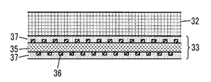
도 2는 실시형태 1의 터치 패널용 도전 필름 적층체를 나타내는 부분 단면도이다.
도 3은 실시형태 1의 터치 패널용 도전 필름 적층체의 도전 필름을 나타내는 평면도이다.
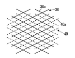
도 4는 도전 필름의 검출 전극을 나타내는 부분 평면도이다.
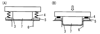
도 5는 벌징 가공을 설명하기 위한 단면도이다.
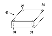
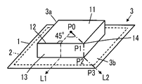
도 6은 각통(角筒) 형상으로 벌징 가공된 실시형태 1의 터치 패널용 도전 필름 적층체를 나타내는 사시도이다.
도 7은 실시형태 1의 터치 패널용 도전 필름 적층체로 성형된 터치 패널을 나타내는 사시도이다.
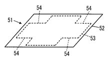
도 8은 실시형태 2에 관한 터치 패널용 도전 필름 적층체를 나타내는 사시도이다.
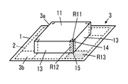
도 9는 각통 형상으로 디프 드로잉 가공된 실시형태 2의 터치 패널용 도전 필름 적층체를 나타내는 사시도이다.
도 10은 디프 드로잉 가공을 설명하기 위한 단면도이다.
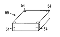
도 11은 실시형태 2의 터치 패널용 도전 필름 적층체로 성형된 터치 패널을 나타내는 사시도이다.
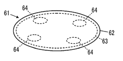
도 12는 실시형태 3에 관한 터치 패널용 도전 필름 적층체를 나타내는 사시도이다.
도 13은 원통 형상으로 벌징 가공된 실시형태 3의 터치 패널용 도전 필름 적층체를 나타내는 사시도이다.
도 14는 실시형태 3의 터치 패널용 도전 필름 적층체로 성형된 터치 패널을 나타내는 사시도이다.
도 15는 실시형태 4에 관한 터치 패널용 도전 필름 적층체를 나타내는 사시도이다.
도 16은 원통 형상으로 디프 드로잉 가공된 실시형태 4의 터치 패널용 도전 필름 적층체를 나타내는 사시도이다.
도 17은 실시형태 4의 터치 패널용 도전 필름 적층체로 성형된 터치 패널을 나타내는 사시도이다.
도 18은 각통 형상으로 프레스 성형된 터치 패널용 도전 필름 적층체의 필름 두께의 측정 개소를 나타내는 도이다.
도 19는 벌징 가공된 터치 패널용 도전 필름 적층체 및 디프 드로잉 가공된 터치 패널용 도전 필름 적층체의 필름 두께 분포를 나타내는 그래프이다.
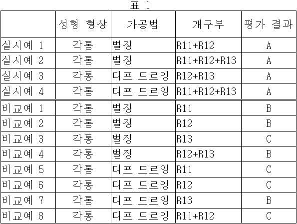
도 20은 각통 형상으로 프레스 성형할 때의 도전 필름의 개구부의 형성 장소를 나타내는 도이다.
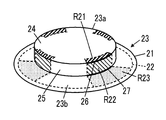
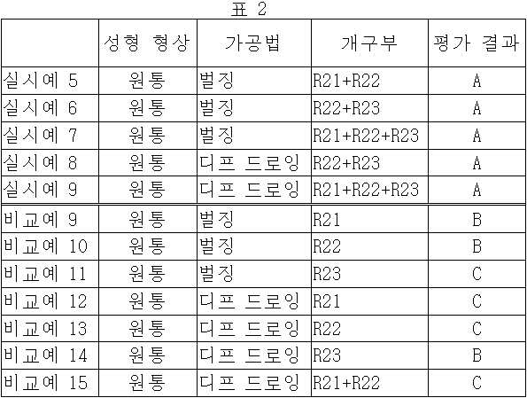
도 21은 원통 형상으로 프레스 성형할 때의 도전 필름의 개구부의 형성 장소를 나타내는 도이다.
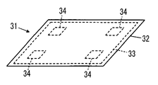
2, 22, 33, 53, 63, 73 도전 필름
3, 23, 31, 51, 61, 71 터치 패널용 도전 필름 적층체
3a, 23a, 51a, 61a, 71a 성형 부분
3b, 23b, 51b, 61b, 71b 플랜지 부분
4 스프링
5 블랭크 홀더
6 하형
7 상형
11, 24, 42, 57, 65, 75 상면
12 변
13, 25, 44, 55, 66, 76 측면
14, 58 꼭짓점
15 교점
26, 27, 67, 68, 77, 78 경계선
34, 54, 64, 74 개구부
35 절연 기판
36 도전 부재
37 보호층
38 제1 검출 전극
38a, 40a 금속 세선
39 제1 주변 배선
40 제2 검출 전극
41 제2 주변 배선
43 꼭짓점
45, 59, 69, 79 터치 패널
56 교점
L1, L2 측정선
P0~P3 측정점
R11~R13, R21~R23 영역
S1 센싱 영역
S2 주변 영역
D1 제1 방향
D2 제2 방향
Claims (16)
- 3차원 형상의 도전체를 성형하기 위한 도전 필름 적층체로서,
평판 형상을 갖는 절연성의 지지체와,
상기 지지체의 표면 상에 접착제로 접합된 도전 필름
을 구비하며,
상기 도전 필름은, 가요성을 갖는 절연 기판과, 상기 절연 기판의 표면 상에 배치된 도전막을 갖고,
상기 절연 기판은, 상기 도전체를 성형할 때에 성형 변형이 집중되는 부분이 잘려 나간 적어도 하나의 개구부를 가지며, 상기 개구부가 상기 지지체에 의하여 막혀 있는 것을 특징으로 하는 도전 필름 적층체. - 청구항 1에 있어서,
상기 도전체를 성형했을 때에, 3차원 형상으로 성형되는 성형 부분과 상기 성형 부분의 주변의 플랜지 부분이 형성되고, 상기 성형 부분이, 상면과, 상기 상면에 접속되는 적어도 하나의 측면을 갖는 경우에,
상기 도전 필름의 상기 개구부는, 상기 성형 부분의 상기 상면과 상기 측면의 사이의 경계부의 일부를 포함하도록 배치되어 있는 도전 필름 적층체. - 청구항 2에 있어서,
상기 성형 부분은, 다각형의 상기 상면과 복수의 상기 측면을 갖고,
상기 도전 필름은, 상기 상면의 복수의 꼭짓점에 대응하는 복수의 상기 개구부를 가지며,
각각의 상기 개구부는, 대응하는 상기 꼭짓점에서 교차하는 상기 상면 및 한 쌍의 상기 측면이 대응하는 상기 꼭짓점을 포함하도록 배치되어 있는 도전 필름 적층체. - 청구항 2에 있어서,
상기 성형 부분은, 원형 또는 타원형의 상기 상면과 하나의 상기 측면을 갖고,
상기 도전 필름은, 상기 상면과 상기 측면의 사이의 환 형상의 경계부의 복수 개소에 있어서의 경계선에 각각 대응하는 복수의 상기 개구부를 가지며,
각각의 상기 개구부는, 상기 상면 및 상기 측면이 대응하는 상기 경계선을 포함하도록 배치되어 있는 도전 필름 적층체. - 청구항 2 내지 청구항 4 중 어느 한 항에 있어서,
상기 개구부는, 관통 구멍으로 이루어지는 도전 필름 적층체. - 청구항 2 내지 청구항 5 중 어느 한 항에 있어서,
상기 성형이, 벌징 가공인 도전 필름 적층체. - 청구항 1에 있어서,
상기 도전체를 성형했을 때에, 3차원 형상으로 성형되는 성형 부분과 상기 성형 부분의 주변의 플랜지 부분이 형성되고, 상기 성형 부분이, 상면과, 상기 상면에 접속되는 적어도 하나의 측면을 가지며,
상기 도전 필름의 상기 개구부는, 상기 성형 부분의 상기 측면과 상기 플랜지 부분의 경계부의 일부를 포함하도록 배치되어 있는 도전 필름 적층체. - 청구항 7에 있어서,
상기 성형 부분은, 다각형의 상기 상면과 복수의 상기 측면을 갖고,
상기 도전 필름은, 각각 상기 성형 부분의 서로 인접하는 한 쌍의 상기 측면과 상기 플랜지 부분이 교차하는 복수의 교점에 대응하는 복수의 상기 개구부를 가지며,
각각의 상기 개구부는, 대응하는 상기 교점에서 교차하는 상기 성형 부분의 한 쌍의 상기 측면 및 상기 플랜지 부분이 대응하는 상기 교점을 포함하도록 배치되어 있는 도전 필름 적층체. - 청구항 7에 있어서,
상기 성형 부분은, 원형 또는 타원형의 상기 상면과 하나의 상기 측면을 갖고,
상기 도전 필름은, 상기 측면과 상기 플랜지 부분의 사이의 환 형상의 경계부의 복수 개소에 있어서의 경계선에 각각 대응하는 복수의 상기 개구부를 가지며,
각각의 상기 개구부는, 상기 성형 부분의 상기 측면 및 상기 플랜지 부분이 대응하는 상기 경계선을 포함하도록 배치되어 있는 도전 필름 적층체. - 청구항 7 내지 청구항 9 중 어느 한 항에 있어서,
상기 개구부는, 노치로 이루어지는 도전 필름 적층체. - 청구항 7 내지 청구항 10 중 어느 한 항에 있어서,
상기 성형이, 디프 드로잉 가공인 도전 필름 적층체. - 청구항 1 내지 청구항 11 중 어느 한 항에 있어서,
상기 지지체 및 상기 절연 기판은, 투명성을 가지며,
상기 도전막은, 상기 절연 기판 중 적어도 한쪽 면 상에 배치되고 또한 금속 세선으로 이루어지는 메시 패턴을 갖는 복수의 검출 전극을 포함하며,
터치 패널에 이용되는 도전 필름 적층체. - 청구항 1 내지 청구항 12 중 어느 한 항에 기재된 도전 필름 적층체를 3차원 형상으로 성형한 도전체.
- 청구항 1 내지 청구항 12 중 어느 한 항에 기재된 도전 필름 적층체를 3차원 형상으로 프레스 성형하고,
프레스 성형된 상기 도전 필름 적층체의 불필요한 부분을 절제하는
도전체의 제조 방법. - 청구항 14에 있어서,
청구항 2 내지 청구항 5 중 어느 한 항에 기재된 도전 필름 적층체를 3차원 형상으로 벌징 가공하고,
벌징 가공된 상기 도전 필름 적층체의 상기 플랜지 부분을 상기 불필요한 부분으로서 절제하는 도전체의 제조 방법. - 청구항 14에 있어서,
청구항 7 내지 청구항 10 중 어느 한 항에 기재된 도전 필름 적층체를 3차원 형상으로 디프 드로잉 가공하고,
디프 드로잉 가공된 상기 도전 필름 적층체의 상기 플랜지 부분을 상기 불필요한 부분으로서 절제하는 도전체의 제조 방법.
Applications Claiming Priority (3)
| Application Number | Priority Date | Filing Date | Title |
|---|---|---|---|
| JPJP-P-2014-180016 | 2014-09-04 | ||
| JP2014180016 | 2014-09-04 | ||
| PCT/JP2015/073082 WO2016035542A1 (ja) | 2014-09-04 | 2015-08-18 | 導電フィルム積層体、導電体および導電体の製造方法 |
Publications (2)
| Publication Number | Publication Date |
|---|---|
| KR20170036742A true KR20170036742A (ko) | 2017-04-03 |
| KR102084298B1 KR102084298B1 (ko) | 2020-03-03 |
Family
ID=55439608
Family Applications (1)
| Application Number | Title | Priority Date | Filing Date |
|---|---|---|---|
| KR1020177005031A Expired - Fee Related KR102084298B1 (ko) | 2014-09-04 | 2015-08-18 | 도전 필름 적층체, 도전체 및 도전체의 제조 방법 |
Country Status (6)
| Country | Link |
|---|---|
| US (1) | US20170136727A1 (ko) |
| JP (1) | JP6317819B2 (ko) |
| KR (1) | KR102084298B1 (ko) |
| CN (1) | CN106662947A (ko) |
| TW (1) | TWI676922B (ko) |
| WO (1) | WO2016035542A1 (ko) |
Families Citing this family (9)
| Publication number | Priority date | Publication date | Assignee | Title |
|---|---|---|---|---|
| WO2016199446A1 (ja) * | 2015-06-11 | 2016-12-15 | 富士フイルム株式会社 | タッチパネル用導電体の製造方法、導電フィルム積層体およびタッチパネル用導電体 |
| JP6445420B2 (ja) * | 2015-12-24 | 2018-12-26 | 富士フイルム株式会社 | 導電フィルム積層体、タッチセンサーおよびタッチセンサーの製造方法 |
| CN107037923B (zh) * | 2017-03-02 | 2020-08-07 | 业成科技(成都)有限公司 | 具双轴心曲面之触控面板的贴合结构 |
| CN110325664A (zh) * | 2017-03-15 | 2019-10-11 | 富士胶片株式会社 | 导电性层叠体的制造方法、导电性层叠体及触摸传感器 |
| CN109508106B (zh) * | 2017-09-15 | 2020-08-28 | 京东方科技集团股份有限公司 | 一种触控面板、其制作方法及触摸屏 |
| KR102420525B1 (ko) * | 2018-01-10 | 2022-07-14 | 삼성디스플레이 주식회사 | 디지타이저 어셈블리의 제조 방법, 이를 이용한 표시 장치의 제조 방법 및 표시 장치 |
| CN108260235B (zh) * | 2018-01-18 | 2022-04-05 | 北京吉泰亿阳科技有限公司 | 一种三维异形电加热膜及其制备方法 |
| CN108376038B (zh) * | 2018-01-18 | 2020-11-20 | 深圳市志凌伟业技术股份有限公司 | 可饶式透明基板做单面架桥sito触控面板制造方法 |
| DE102019127108A1 (de) * | 2019-10-09 | 2021-04-15 | Leonhard Kurz Stiftung & Co. Kg | Verfahren und Vorrichtung zur Herstellung eines Kunststoffbauteils sowie ein Kunststoffbauteil |
Citations (7)
| Publication number | Priority date | Publication date | Assignee | Title |
|---|---|---|---|---|
| US20100103138A1 (en) * | 2008-10-27 | 2010-04-29 | Tpk Touch Solutions Inc. | Curved capacitive touch panel and manufacture method thereof |
| US20120218219A1 (en) * | 2011-02-28 | 2012-08-30 | Rappoport Benjamin M | Displays with minimized borders |
| US20130162596A1 (en) * | 2010-10-18 | 2013-06-27 | Gunze Limited | Touch switch |
| JP2013131129A (ja) * | 2011-12-22 | 2013-07-04 | Nissha Printing Co Ltd | 装飾付きタッチセンサ及びその製造方法 |
| WO2013187123A1 (ja) * | 2012-06-14 | 2013-12-19 | 日本写真印刷株式会社 | タッチパネルの製造方法及び導電電極付フィルム |
| JP2014035754A (ja) * | 2012-08-10 | 2014-02-24 | Nissha Printing Co Ltd | タッチセンサ及び電子機器 |
| US20140104185A1 (en) * | 2012-10-15 | 2014-04-17 | Htc Corporation | Touch display device and handheld electronic device |
Family Cites Families (6)
| Publication number | Priority date | Publication date | Assignee | Title |
|---|---|---|---|---|
| JP4924393B2 (ja) * | 2007-12-05 | 2012-04-25 | ソニー株式会社 | ディスプレイ装置 |
| TWI465794B (zh) * | 2010-02-08 | 2014-12-21 | Ind Tech Res Inst | 觸控面板捲及其製造方法 |
| CN103189820B (zh) * | 2010-10-21 | 2016-04-20 | 京瓷株式会社 | 触摸面板设备 |
| CN103329642B (zh) * | 2011-01-18 | 2018-01-02 | 富士胶片株式会社 | 导电膜和设置有该导电膜的显示装置 |
| US10061356B2 (en) * | 2011-06-30 | 2018-08-28 | Samsung Display Co., Ltd. | Flexible display panel and display apparatus including the flexible display panel |
| JP5721601B2 (ja) * | 2011-09-30 | 2015-05-20 | 富士フイルム株式会社 | タッチパネル、及びタッチパネルの製造方法 |
-
2015
- 2015-08-18 CN CN201580039251.3A patent/CN106662947A/zh active Pending
- 2015-08-18 WO PCT/JP2015/073082 patent/WO2016035542A1/ja not_active Ceased
- 2015-08-18 KR KR1020177005031A patent/KR102084298B1/ko not_active Expired - Fee Related
- 2015-08-18 JP JP2016546405A patent/JP6317819B2/ja not_active Expired - Fee Related
- 2015-08-25 TW TW104127648A patent/TWI676922B/zh not_active IP Right Cessation
-
2017
- 2017-01-31 US US15/420,180 patent/US20170136727A1/en not_active Abandoned
Patent Citations (8)
| Publication number | Priority date | Publication date | Assignee | Title |
|---|---|---|---|---|
| US20100103138A1 (en) * | 2008-10-27 | 2010-04-29 | Tpk Touch Solutions Inc. | Curved capacitive touch panel and manufacture method thereof |
| US20130162596A1 (en) * | 2010-10-18 | 2013-06-27 | Gunze Limited | Touch switch |
| US20120218219A1 (en) * | 2011-02-28 | 2012-08-30 | Rappoport Benjamin M | Displays with minimized borders |
| JP2013131129A (ja) * | 2011-12-22 | 2013-07-04 | Nissha Printing Co Ltd | 装飾付きタッチセンサ及びその製造方法 |
| WO2013187123A1 (ja) * | 2012-06-14 | 2013-12-19 | 日本写真印刷株式会社 | タッチパネルの製造方法及び導電電極付フィルム |
| JP2013257796A (ja) | 2012-06-14 | 2013-12-26 | Nissha Printing Co Ltd | タッチパネルの製造方法及び導電電極付フィルム |
| JP2014035754A (ja) * | 2012-08-10 | 2014-02-24 | Nissha Printing Co Ltd | タッチセンサ及び電子機器 |
| US20140104185A1 (en) * | 2012-10-15 | 2014-04-17 | Htc Corporation | Touch display device and handheld electronic device |
Also Published As
| Publication number | Publication date |
|---|---|
| JP6317819B2 (ja) | 2018-04-25 |
| CN106662947A (zh) | 2017-05-10 |
| US20170136727A1 (en) | 2017-05-18 |
| KR102084298B1 (ko) | 2020-03-03 |
| TWI676922B (zh) | 2019-11-11 |
| JPWO2016035542A1 (ja) | 2017-04-27 |
| WO2016035542A1 (ja) | 2016-03-10 |
| TW201610785A (zh) | 2016-03-16 |
Similar Documents
| Publication | Publication Date | Title |
|---|---|---|
| JP6317819B2 (ja) | 導電フィルム積層体、導電体および導電体の製造方法 | |
| US8658907B2 (en) | Conductive film and method for producing the same | |
| JP6240789B2 (ja) | タッチパネル用導電フィルムおよびタッチパネル | |
| CN107710122B (zh) | 触摸面板用导电薄膜的网格图案设计方法、触摸面板用导电薄膜的制造方法及触摸面板用导电薄膜 | |
| TWI621043B (zh) | 層積結構體和觸控式螢幕模組 | |
| CN105190497A (zh) | 触控面板用导电片材的制造方法和触控面板用导电片材 | |
| CN110383222A (zh) | 导电性部件及触摸面板 | |
| KR20180015748A (ko) | 터치 패널용 도전 필름, 터치 패널, 및 터치 패널 부착 표시 장치 | |
| EP2796971A1 (en) | Conductive sheet and touch panel | |
| TWI668710B (zh) | Method for forming electric conductor and electric conductor | |
| JP6445420B2 (ja) | 導電フィルム積層体、タッチセンサーおよびタッチセンサーの製造方法 | |
| JP6445694B2 (ja) | タッチパネル用導電体の製造方法、導電フィルム積層体およびタッチパネル用導電体 | |
| TWI708170B (zh) | 透明導電膜、透明導電膜的製造方法及觸控感測器 | |
| JP6588992B2 (ja) | 導電フィルム積層体 | |
| JP5463315B2 (ja) | 電極シート、電極シートの製造方法、及びタッチパネル | |
| JP2020194196A (ja) | タッチパネル用導電性フィルム、導電性部材およびタッチパネル | |
| WO2015029734A1 (ja) | 導電シート及びタッチパネル |
Legal Events
| Date | Code | Title | Description |
|---|---|---|---|
| A201 | Request for examination | ||
| P11-X000 | Amendment of application requested |
St.27 status event code: A-2-2-P10-P11-nap-X000 |
|
| P13-X000 | Application amended |
St.27 status event code: A-2-2-P10-P13-nap-X000 |
|
| PA0105 | International application |
St.27 status event code: A-0-1-A10-A15-nap-PA0105 |
|
| PA0201 | Request for examination |
St.27 status event code: A-1-2-D10-D11-exm-PA0201 |
|
| PG1501 | Laying open of application |
St.27 status event code: A-1-1-Q10-Q12-nap-PG1501 |
|
| D13-X000 | Search requested |
St.27 status event code: A-1-2-D10-D13-srh-X000 |
|
| D14-X000 | Search report completed |
St.27 status event code: A-1-2-D10-D14-srh-X000 |
|
| E902 | Notification of reason for refusal | ||
| PE0902 | Notice of grounds for rejection |
St.27 status event code: A-1-2-D10-D21-exm-PE0902 |
|
| P11-X000 | Amendment of application requested |
St.27 status event code: A-2-2-P10-P11-nap-X000 |
|
| P13-X000 | Application amended |
St.27 status event code: A-2-2-P10-P13-nap-X000 |
|
| E902 | Notification of reason for refusal | ||
| PE0902 | Notice of grounds for rejection |
St.27 status event code: A-1-2-D10-D21-exm-PE0902 |
|
| P11-X000 | Amendment of application requested |
St.27 status event code: A-2-2-P10-P11-nap-X000 |
|
| P13-X000 | Application amended |
St.27 status event code: A-2-2-P10-P13-nap-X000 |
|
| P22-X000 | Classification modified |
St.27 status event code: A-2-2-P10-P22-nap-X000 |
|
| E90F | Notification of reason for final refusal | ||
| PE0902 | Notice of grounds for rejection |
St.27 status event code: A-1-2-D10-D21-exm-PE0902 |
|
| P11-X000 | Amendment of application requested |
St.27 status event code: A-2-2-P10-P11-nap-X000 |
|
| P13-X000 | Application amended |
St.27 status event code: A-2-2-P10-P13-nap-X000 |
|
| E701 | Decision to grant or registration of patent right | ||
| PE0701 | Decision of registration |
St.27 status event code: A-1-2-D10-D22-exm-PE0701 |
|
| GRNT | Written decision to grant | ||
| PR0701 | Registration of establishment |
St.27 status event code: A-2-4-F10-F11-exm-PR0701 |
|
| PR1002 | Payment of registration fee |
St.27 status event code: A-2-2-U10-U12-oth-PR1002 Fee payment year number: 1 |
|
| PG1601 | Publication of registration |
St.27 status event code: A-4-4-Q10-Q13-nap-PG1601 |
|
| P22-X000 | Classification modified |
St.27 status event code: A-4-4-P10-P22-nap-X000 |
|
| PC1903 | Unpaid annual fee |
St.27 status event code: A-4-4-U10-U13-oth-PC1903 Not in force date: 20230227 Payment event data comment text: Termination Category : DEFAULT_OF_REGISTRATION_FEE |
|
| PC1903 | Unpaid annual fee |
St.27 status event code: N-4-6-H10-H13-oth-PC1903 Ip right cessation event data comment text: Termination Category : DEFAULT_OF_REGISTRATION_FEE Not in force date: 20230227 |