KR20170042500A - 방향족 메틸올 화합물이 반응된 노볼락 수지를 포함하는 레지스트 하층막 형성 조성물 - Google Patents
방향족 메틸올 화합물이 반응된 노볼락 수지를 포함하는 레지스트 하층막 형성 조성물 Download PDFInfo
- Publication number
- KR20170042500A KR20170042500A KR1020167032229A KR20167032229A KR20170042500A KR 20170042500 A KR20170042500 A KR 20170042500A KR 1020167032229 A KR1020167032229 A KR 1020167032229A KR 20167032229 A KR20167032229 A KR 20167032229A KR 20170042500 A KR20170042500 A KR 20170042500A
- Authority
- KR
- South Korea
- Prior art keywords
- group
- resist
- lower layer
- forming
- layer film
- Prior art date
- Legal status (The legal status is an assumption and is not a legal conclusion. Google has not performed a legal analysis and makes no representation as to the accuracy of the status listed.)
- Granted
Links
Classifications
-
- G—PHYSICS
- G03—PHOTOGRAPHY; CINEMATOGRAPHY; ANALOGOUS TECHNIQUES USING WAVES OTHER THAN OPTICAL WAVES; ELECTROGRAPHY; HOLOGRAPHY
- G03F—PHOTOMECHANICAL PRODUCTION OF TEXTURED OR PATTERNED SURFACES, e.g. FOR PRINTING, FOR PROCESSING OF SEMICONDUCTOR DEVICES; MATERIALS THEREFOR; ORIGINALS THEREFOR; APPARATUS SPECIALLY ADAPTED THEREFOR
- G03F7/00—Photomechanical, e.g. photolithographic, production of textured or patterned surfaces, e.g. printing surfaces; Materials therefor, e.g. comprising photoresists; Apparatus specially adapted therefor
- G03F7/004—Photosensitive materials
- G03F7/09—Photosensitive materials characterised by structural details, e.g. supports, auxiliary layers
- G03F7/11—Photosensitive materials characterised by structural details, e.g. supports, auxiliary layers having cover layers or intermediate layers, e.g. subbing layers
-
- C—CHEMISTRY; METALLURGY
- C08—ORGANIC MACROMOLECULAR COMPOUNDS; THEIR PREPARATION OR CHEMICAL WORKING-UP; COMPOSITIONS BASED THEREON
- C08G—MACROMOLECULAR COMPOUNDS OBTAINED OTHERWISE THAN BY REACTIONS ONLY INVOLVING UNSATURATED CARBON-TO-CARBON BONDS
- C08G12/00—Condensation polymers of aldehydes or ketones with only compounds containing hydrogen attached to nitrogen
- C08G12/02—Condensation polymers of aldehydes or ketones with only compounds containing hydrogen attached to nitrogen of aldehydes
- C08G12/26—Condensation polymers of aldehydes or ketones with only compounds containing hydrogen attached to nitrogen of aldehydes with heterocyclic compounds
-
- C—CHEMISTRY; METALLURGY
- C08—ORGANIC MACROMOLECULAR COMPOUNDS; THEIR PREPARATION OR CHEMICAL WORKING-UP; COMPOSITIONS BASED THEREON
- C08G—MACROMOLECULAR COMPOUNDS OBTAINED OTHERWISE THAN BY REACTIONS ONLY INVOLVING UNSATURATED CARBON-TO-CARBON BONDS
- C08G14/00—Condensation polymers of aldehydes or ketones with two or more other monomers covered by at least two of the groups C08G8/00 - C08G12/00
- C08G14/02—Condensation polymers of aldehydes or ketones with two or more other monomers covered by at least two of the groups C08G8/00 - C08G12/00 of aldehydes
- C08G14/04—Condensation polymers of aldehydes or ketones with two or more other monomers covered by at least two of the groups C08G8/00 - C08G12/00 of aldehydes with phenols
- C08G14/06—Condensation polymers of aldehydes or ketones with two or more other monomers covered by at least two of the groups C08G8/00 - C08G12/00 of aldehydes with phenols and monomers containing hydrogen attached to nitrogen
-
- C—CHEMISTRY; METALLURGY
- C08—ORGANIC MACROMOLECULAR COMPOUNDS; THEIR PREPARATION OR CHEMICAL WORKING-UP; COMPOSITIONS BASED THEREON
- C08G—MACROMOLECULAR COMPOUNDS OBTAINED OTHERWISE THAN BY REACTIONS ONLY INVOLVING UNSATURATED CARBON-TO-CARBON BONDS
- C08G8/00—Condensation polymers of aldehydes or ketones with phenols only
- C08G8/04—Condensation polymers of aldehydes or ketones with phenols only of aldehydes
- C08G8/08—Condensation polymers of aldehydes or ketones with phenols only of aldehydes of formaldehyde, e.g. of formaldehyde formed in situ
- C08G8/24—Condensation polymers of aldehydes or ketones with phenols only of aldehydes of formaldehyde, e.g. of formaldehyde formed in situ with mixtures of two or more phenols which are not covered by only one of the groups C08G8/10 - C08G8/20
-
- C—CHEMISTRY; METALLURGY
- C09—DYES; PAINTS; POLISHES; NATURAL RESINS; ADHESIVES; COMPOSITIONS NOT OTHERWISE PROVIDED FOR; APPLICATIONS OF MATERIALS NOT OTHERWISE PROVIDED FOR
- C09D—COATING COMPOSITIONS, e.g. PAINTS, VARNISHES OR LACQUERS; FILLING PASTES; CHEMICAL PAINT OR INK REMOVERS; INKS; CORRECTING FLUIDS; WOODSTAINS; PASTES OR SOLIDS FOR COLOURING OR PRINTING; USE OF MATERIALS THEREFOR
- C09D161/00—Coating compositions based on condensation polymers of aldehydes or ketones; Coating compositions based on derivatives of such polymers
- C09D161/34—Condensation polymers of aldehydes or ketones with monomers covered by at least two of the groups C09D161/04, C09D161/18 and C09D161/20
-
- G—PHYSICS
- G03—PHOTOGRAPHY; CINEMATOGRAPHY; ANALOGOUS TECHNIQUES USING WAVES OTHER THAN OPTICAL WAVES; ELECTROGRAPHY; HOLOGRAPHY
- G03F—PHOTOMECHANICAL PRODUCTION OF TEXTURED OR PATTERNED SURFACES, e.g. FOR PRINTING, FOR PROCESSING OF SEMICONDUCTOR DEVICES; MATERIALS THEREFOR; ORIGINALS THEREFOR; APPARATUS SPECIALLY ADAPTED THEREFOR
- G03F7/00—Photomechanical, e.g. photolithographic, production of textured or patterned surfaces, e.g. printing surfaces; Materials therefor, e.g. comprising photoresists; Apparatus specially adapted therefor
- G03F7/004—Photosensitive materials
- G03F7/038—Macromolecular compounds which are rendered insoluble or differentially wettable
-
- G—PHYSICS
- G03—PHOTOGRAPHY; CINEMATOGRAPHY; ANALOGOUS TECHNIQUES USING WAVES OTHER THAN OPTICAL WAVES; ELECTROGRAPHY; HOLOGRAPHY
- G03F—PHOTOMECHANICAL PRODUCTION OF TEXTURED OR PATTERNED SURFACES, e.g. FOR PRINTING, FOR PROCESSING OF SEMICONDUCTOR DEVICES; MATERIALS THEREFOR; ORIGINALS THEREFOR; APPARATUS SPECIALLY ADAPTED THEREFOR
- G03F7/00—Photomechanical, e.g. photolithographic, production of textured or patterned surfaces, e.g. printing surfaces; Materials therefor, e.g. comprising photoresists; Apparatus specially adapted therefor
- G03F7/004—Photosensitive materials
- G03F7/039—Macromolecular compounds which are photodegradable, e.g. positive electron resists
-
- G—PHYSICS
- G03—PHOTOGRAPHY; CINEMATOGRAPHY; ANALOGOUS TECHNIQUES USING WAVES OTHER THAN OPTICAL WAVES; ELECTROGRAPHY; HOLOGRAPHY
- G03F—PHOTOMECHANICAL PRODUCTION OF TEXTURED OR PATTERNED SURFACES, e.g. FOR PRINTING, FOR PROCESSING OF SEMICONDUCTOR DEVICES; MATERIALS THEREFOR; ORIGINALS THEREFOR; APPARATUS SPECIALLY ADAPTED THEREFOR
- G03F7/00—Photomechanical, e.g. photolithographic, production of textured or patterned surfaces, e.g. printing surfaces; Materials therefor, e.g. comprising photoresists; Apparatus specially adapted therefor
- G03F7/004—Photosensitive materials
- G03F7/09—Photosensitive materials characterised by structural details, e.g. supports, auxiliary layers
- G03F7/094—Multilayer resist systems, e.g. planarising layers
-
- G—PHYSICS
- G03—PHOTOGRAPHY; CINEMATOGRAPHY; ANALOGOUS TECHNIQUES USING WAVES OTHER THAN OPTICAL WAVES; ELECTROGRAPHY; HOLOGRAPHY
- G03F—PHOTOMECHANICAL PRODUCTION OF TEXTURED OR PATTERNED SURFACES, e.g. FOR PRINTING, FOR PROCESSING OF SEMICONDUCTOR DEVICES; MATERIALS THEREFOR; ORIGINALS THEREFOR; APPARATUS SPECIALLY ADAPTED THEREFOR
- G03F7/00—Photomechanical, e.g. photolithographic, production of textured or patterned surfaces, e.g. printing surfaces; Materials therefor, e.g. comprising photoresists; Apparatus specially adapted therefor
- G03F7/16—Coating processes; Apparatus therefor
- G03F7/162—Coating on a rotating support, e.g. using a whirler or a spinner
-
- G—PHYSICS
- G03—PHOTOGRAPHY; CINEMATOGRAPHY; ANALOGOUS TECHNIQUES USING WAVES OTHER THAN OPTICAL WAVES; ELECTROGRAPHY; HOLOGRAPHY
- G03F—PHOTOMECHANICAL PRODUCTION OF TEXTURED OR PATTERNED SURFACES, e.g. FOR PRINTING, FOR PROCESSING OF SEMICONDUCTOR DEVICES; MATERIALS THEREFOR; ORIGINALS THEREFOR; APPARATUS SPECIALLY ADAPTED THEREFOR
- G03F7/00—Photomechanical, e.g. photolithographic, production of textured or patterned surfaces, e.g. printing surfaces; Materials therefor, e.g. comprising photoresists; Apparatus specially adapted therefor
- G03F7/16—Coating processes; Apparatus therefor
- G03F7/168—Finishing the coated layer, e.g. drying, baking, soaking
-
- G—PHYSICS
- G03—PHOTOGRAPHY; CINEMATOGRAPHY; ANALOGOUS TECHNIQUES USING WAVES OTHER THAN OPTICAL WAVES; ELECTROGRAPHY; HOLOGRAPHY
- G03F—PHOTOMECHANICAL PRODUCTION OF TEXTURED OR PATTERNED SURFACES, e.g. FOR PRINTING, FOR PROCESSING OF SEMICONDUCTOR DEVICES; MATERIALS THEREFOR; ORIGINALS THEREFOR; APPARATUS SPECIALLY ADAPTED THEREFOR
- G03F7/00—Photomechanical, e.g. photolithographic, production of textured or patterned surfaces, e.g. printing surfaces; Materials therefor, e.g. comprising photoresists; Apparatus specially adapted therefor
- G03F7/20—Exposure; Apparatus therefor
- G03F7/2002—Exposure; Apparatus therefor with visible light or UV light, through an original having an opaque pattern on a transparent support, e.g. film printing, projection printing; by reflection of visible or UV light from an original such as a printed image
- G03F7/2004—Exposure; Apparatus therefor with visible light or UV light, through an original having an opaque pattern on a transparent support, e.g. film printing, projection printing; by reflection of visible or UV light from an original such as a printed image characterised by the use of a particular light source, e.g. fluorescent lamps or deep UV light
- G03F7/2006—Exposure; Apparatus therefor with visible light or UV light, through an original having an opaque pattern on a transparent support, e.g. film printing, projection printing; by reflection of visible or UV light from an original such as a printed image characterised by the use of a particular light source, e.g. fluorescent lamps or deep UV light using coherent light; using polarised light
-
- G—PHYSICS
- G03—PHOTOGRAPHY; CINEMATOGRAPHY; ANALOGOUS TECHNIQUES USING WAVES OTHER THAN OPTICAL WAVES; ELECTROGRAPHY; HOLOGRAPHY
- G03F—PHOTOMECHANICAL PRODUCTION OF TEXTURED OR PATTERNED SURFACES, e.g. FOR PRINTING, FOR PROCESSING OF SEMICONDUCTOR DEVICES; MATERIALS THEREFOR; ORIGINALS THEREFOR; APPARATUS SPECIALLY ADAPTED THEREFOR
- G03F7/00—Photomechanical, e.g. photolithographic, production of textured or patterned surfaces, e.g. printing surfaces; Materials therefor, e.g. comprising photoresists; Apparatus specially adapted therefor
- G03F7/20—Exposure; Apparatus therefor
- G03F7/2037—Exposure with X-ray radiation or corpuscular radiation, through a mask with a pattern opaque to that radiation
-
- G—PHYSICS
- G03—PHOTOGRAPHY; CINEMATOGRAPHY; ANALOGOUS TECHNIQUES USING WAVES OTHER THAN OPTICAL WAVES; ELECTROGRAPHY; HOLOGRAPHY
- G03F—PHOTOMECHANICAL PRODUCTION OF TEXTURED OR PATTERNED SURFACES, e.g. FOR PRINTING, FOR PROCESSING OF SEMICONDUCTOR DEVICES; MATERIALS THEREFOR; ORIGINALS THEREFOR; APPARATUS SPECIALLY ADAPTED THEREFOR
- G03F7/00—Photomechanical, e.g. photolithographic, production of textured or patterned surfaces, e.g. printing surfaces; Materials therefor, e.g. comprising photoresists; Apparatus specially adapted therefor
- G03F7/26—Processing photosensitive materials; Apparatus therefor
- G03F7/30—Imagewise removal using liquid means
- G03F7/32—Liquid compositions therefor, e.g. developers
- G03F7/322—Aqueous alkaline compositions
-
- G—PHYSICS
- G03—PHOTOGRAPHY; CINEMATOGRAPHY; ANALOGOUS TECHNIQUES USING WAVES OTHER THAN OPTICAL WAVES; ELECTROGRAPHY; HOLOGRAPHY
- G03F—PHOTOMECHANICAL PRODUCTION OF TEXTURED OR PATTERNED SURFACES, e.g. FOR PRINTING, FOR PROCESSING OF SEMICONDUCTOR DEVICES; MATERIALS THEREFOR; ORIGINALS THEREFOR; APPARATUS SPECIALLY ADAPTED THEREFOR
- G03F7/00—Photomechanical, e.g. photolithographic, production of textured or patterned surfaces, e.g. printing surfaces; Materials therefor, e.g. comprising photoresists; Apparatus specially adapted therefor
- G03F7/26—Processing photosensitive materials; Apparatus therefor
- G03F7/30—Imagewise removal using liquid means
- G03F7/32—Liquid compositions therefor, e.g. developers
- G03F7/325—Non-aqueous compositions
-
- G—PHYSICS
- G03—PHOTOGRAPHY; CINEMATOGRAPHY; ANALOGOUS TECHNIQUES USING WAVES OTHER THAN OPTICAL WAVES; ELECTROGRAPHY; HOLOGRAPHY
- G03F—PHOTOMECHANICAL PRODUCTION OF TEXTURED OR PATTERNED SURFACES, e.g. FOR PRINTING, FOR PROCESSING OF SEMICONDUCTOR DEVICES; MATERIALS THEREFOR; ORIGINALS THEREFOR; APPARATUS SPECIALLY ADAPTED THEREFOR
- G03F7/00—Photomechanical, e.g. photolithographic, production of textured or patterned surfaces, e.g. printing surfaces; Materials therefor, e.g. comprising photoresists; Apparatus specially adapted therefor
- G03F7/26—Processing photosensitive materials; Apparatus therefor
- G03F7/38—Treatment before imagewise removal, e.g. prebaking
-
- H—ELECTRICITY
- H10—SEMICONDUCTOR DEVICES; ELECTRIC SOLID-STATE DEVICES NOT OTHERWISE PROVIDED FOR
- H10P—GENERIC PROCESSES OR APPARATUS FOR THE MANUFACTURE OR TREATMENT OF DEVICES COVERED BY CLASS H10
- H10P50/00—Etching of wafers, substrates or parts of devices
- H10P50/20—Dry etching; Plasma etching; Reactive-ion etching
- H10P50/28—Dry etching; Plasma etching; Reactive-ion etching of insulating materials
- H10P50/282—Dry etching; Plasma etching; Reactive-ion etching of insulating materials of inorganic materials
- H10P50/283—Dry etching; Plasma etching; Reactive-ion etching of insulating materials of inorganic materials by chemical means
-
- H—ELECTRICITY
- H10—SEMICONDUCTOR DEVICES; ELECTRIC SOLID-STATE DEVICES NOT OTHERWISE PROVIDED FOR
- H10P—GENERIC PROCESSES OR APPARATUS FOR THE MANUFACTURE OR TREATMENT OF DEVICES COVERED BY CLASS H10
- H10P50/00—Etching of wafers, substrates or parts of devices
- H10P50/69—Etching of wafers, substrates or parts of devices using masks for semiconductor materials
- H10P50/691—Etching of wafers, substrates or parts of devices using masks for semiconductor materials for Group V materials or Group III-V materials
- H10P50/692—Etching of wafers, substrates or parts of devices using masks for semiconductor materials for Group V materials or Group III-V materials characterised by their composition, e.g. multilayer masks or materials
-
- H—ELECTRICITY
- H10—SEMICONDUCTOR DEVICES; ELECTRIC SOLID-STATE DEVICES NOT OTHERWISE PROVIDED FOR
- H10P—GENERIC PROCESSES OR APPARATUS FOR THE MANUFACTURE OR TREATMENT OF DEVICES COVERED BY CLASS H10
- H10P50/00—Etching of wafers, substrates or parts of devices
- H10P50/69—Etching of wafers, substrates or parts of devices using masks for semiconductor materials
- H10P50/691—Etching of wafers, substrates or parts of devices using masks for semiconductor materials for Group V materials or Group III-V materials
- H10P50/693—Etching of wafers, substrates or parts of devices using masks for semiconductor materials for Group V materials or Group III-V materials characterised by their size, orientation, disposition, behaviour or shape, in horizontal or vertical plane
- H10P50/695—Etching of wafers, substrates or parts of devices using masks for semiconductor materials for Group V materials or Group III-V materials characterised by their size, orientation, disposition, behaviour or shape, in horizontal or vertical plane characterised by the process involved to create the mask, e.g. lift-off masks or sidewalls or to modify the mask
-
- H—ELECTRICITY
- H10—SEMICONDUCTOR DEVICES; ELECTRIC SOLID-STATE DEVICES NOT OTHERWISE PROVIDED FOR
- H10P—GENERIC PROCESSES OR APPARATUS FOR THE MANUFACTURE OR TREATMENT OF DEVICES COVERED BY CLASS H10
- H10P50/00—Etching of wafers, substrates or parts of devices
- H10P50/73—Etching of wafers, substrates or parts of devices using masks for insulating materials
Landscapes
- Physics & Mathematics (AREA)
- Chemical & Material Sciences (AREA)
- General Physics & Mathematics (AREA)
- Organic Chemistry (AREA)
- Engineering & Computer Science (AREA)
- Health & Medical Sciences (AREA)
- Chemical Kinetics & Catalysis (AREA)
- Medicinal Chemistry (AREA)
- Polymers & Plastics (AREA)
- Architecture (AREA)
- Structural Engineering (AREA)
- Spectroscopy & Molecular Physics (AREA)
- Life Sciences & Earth Sciences (AREA)
- Materials Engineering (AREA)
- Wood Science & Technology (AREA)
- Materials For Photolithography (AREA)
- Photosensitive Polymer And Photoresist Processing (AREA)
- Exposure And Positioning Against Photoresist Photosensitive Materials (AREA)
- Phenolic Resins Or Amino Resins (AREA)
- Exposure Of Semiconductors, Excluding Electron Or Ion Beam Exposure (AREA)
Abstract
[해결수단] 방향족 화합물(A)의 방향족환과 하이드록시기 함유 방향족 메틸올 화합물(B)와의 반응에 의해 얻어지는 구조체(C)를 포함하는 노볼락 수지를 포함하는 레지스트 하층막 형성 조성물. 방향족 화합물(A)가 노볼락 수지에 포함되는 구조체(C)를 구성하기 위한 성분이다. 하이드록시기 함유 방향족 메틸올 화합물(B)가 식(1):

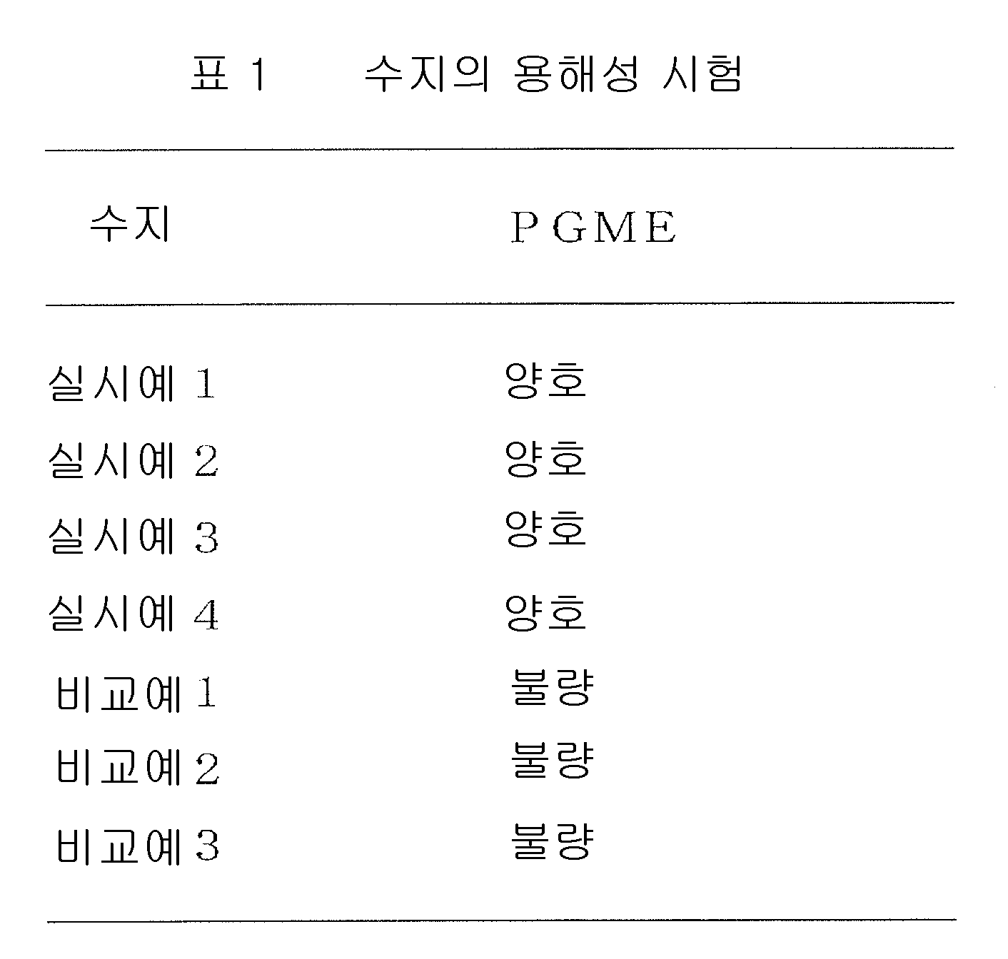
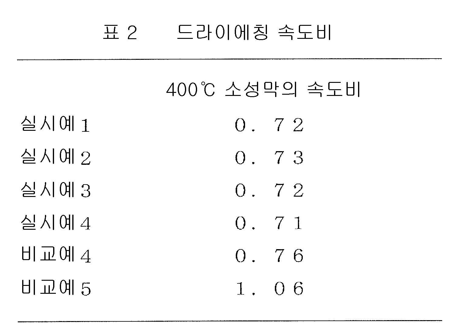
로 표시된다. 하이드록시기 함유 방향족 메틸올 화합물(B)가 2-하이드록시벤질알코올, 4-하이드록시벤질알코올, 또는 2,6-디-tert-부틸-4-하이드록시메틸페놀이다.
Description


Claims (17)
- 방향족 화합물(A)의 방향족환과 하이드록시기 함유 방향족 메틸올 화합물(B)와의 반응에 의해 얻어지는 구조체(C)를 포함하는 노볼락 수지를 포함하는 레지스트 하층막 형성 조성물.
- 제1항에 있어서,
상기 방향족 화합물(A)가 노볼락 수지에 포함되는 구조체(C)를 구성하기 위한 성분인 레지스트 하층막 형성 조성물.
- 제1항 또는 제2항에 있어서,
상기 하이드록시기 함유 방향족 메틸올 화합물(B)가 식(1):
[화학식 1]

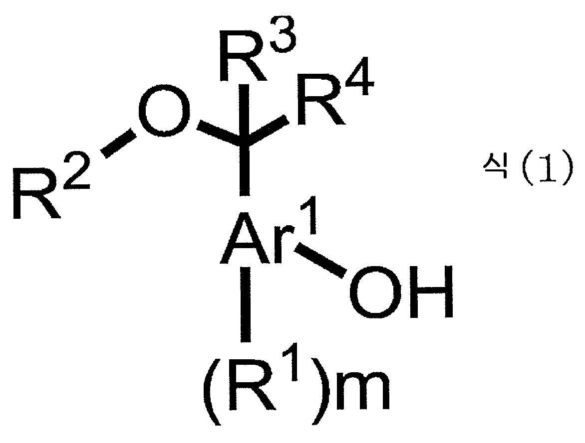
(식(1) 중, Ar1은 탄소원자수 6 내지 40의 아릴기를 나타내고, R1은 탄소원자수 1 내지 10의 알킬기, 탄소원자수 2 내지 10의 알케닐기, 탄소원자수 2 내지 10의 알키닐기, 탄소원자수 6 내지 40의 아릴기, 하이드록시기, 시아노기, 니트로기, 아미노기, 카르복실기, 아세틸기, 헬로게노메틸기, -Y-Z기, 할로겐원자, 또는 이들의 조합을 나타낸다. Y는 산소원자, 황원자, 카르보닐기, 또는 에스테르기를 나타내고, Z는 탄소원자수 1 내지 10의 알킬기를 나타낸다. R2는 수소원자 또는 메틸기를 나타낸다. R3, R4는 각각 수소원자, 탄소원자수 1 내지 10의 알킬기, 탄소원자수 2 내지 10의 알케닐기, 시아노기, 또는 알킬아미노기를 나타낸다. m은 0 내지 (4+2n)의 정수이고, n은 아릴기 Ar1이 가지는 벤젠환의 축합도를 나타낸다.)로 표시되는 화합물인 레지스트 하층막 형성 조성물.
- 제1항 내지 제3항 중 어느 한 항에 있어서,
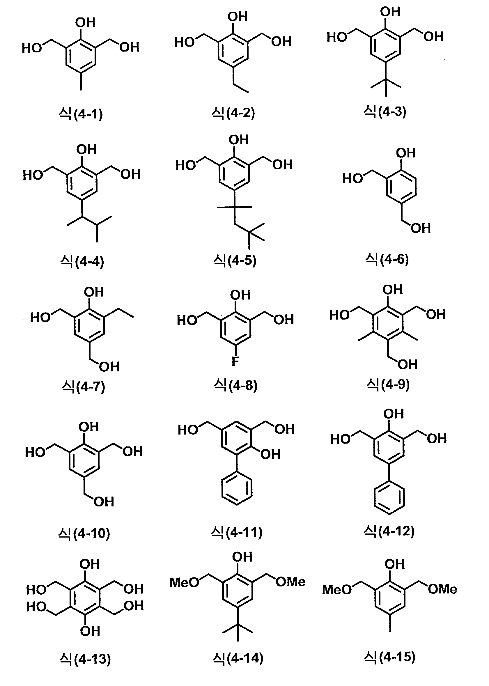
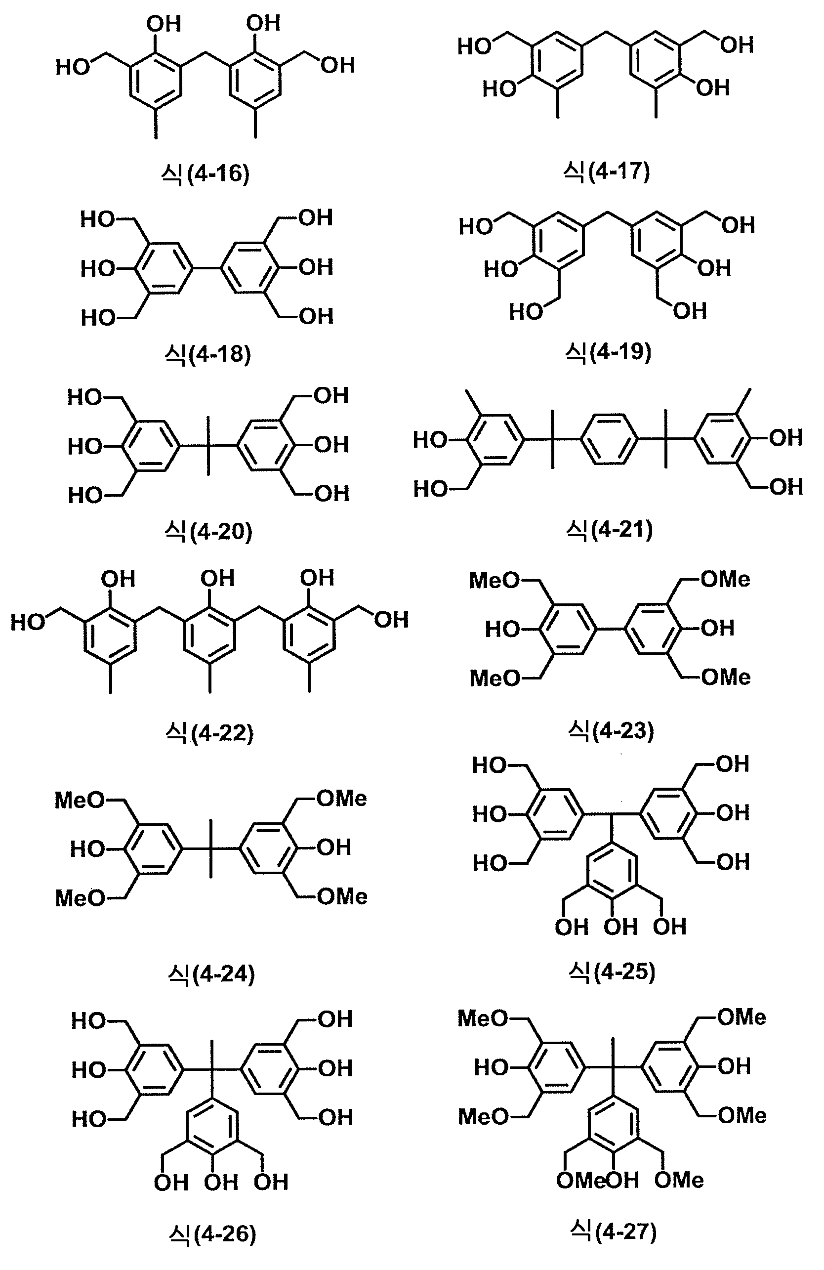
상기 하이드록시기 함유 방향족 메틸올 화합물(B)가 2-하이드록시벤질알코올, 4-하이드록시벤질알코올, 또는 2,6-디-tert-부틸-4-하이드록시메틸페놀인 레지스트 하층막 형성 조성물.
- 제1항 내지 제4항 중 어느 한 항에 있어서,
상기 구조체(C)가 식(2):
[화학식 2]
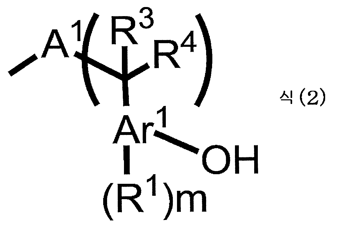
(식(2) 중, Ar1, R1, R3, R4 및 m은 식(1)과 동일하고, A1은 방향족 화합물(A)의 방향족환 또는 노볼락 수지의 방향족환이다.)로 표시되는 구조를 가지는 레지스트 하층막 형성 조성물.
- 제1항 내지 제5항 중 어느 한 항에 있어서,
상기 방향족 화합물(A)가 방향족 아민 또는 페놀성 하이드록시기 함유 화합물인 레지스트 하층막 형성 조성물.
- 제1항 내지 제6항 중 어느 한 항에 있어서,
상기 노볼락 수지가, 방향족 아민 또는 페놀성 하이드록시기 함유 화합물과, 알데하이드 또는 케톤과의 반응에 의해 생성된 수지인 레지스트 하층막 형성 조성물.
- 제7항에 있어서,
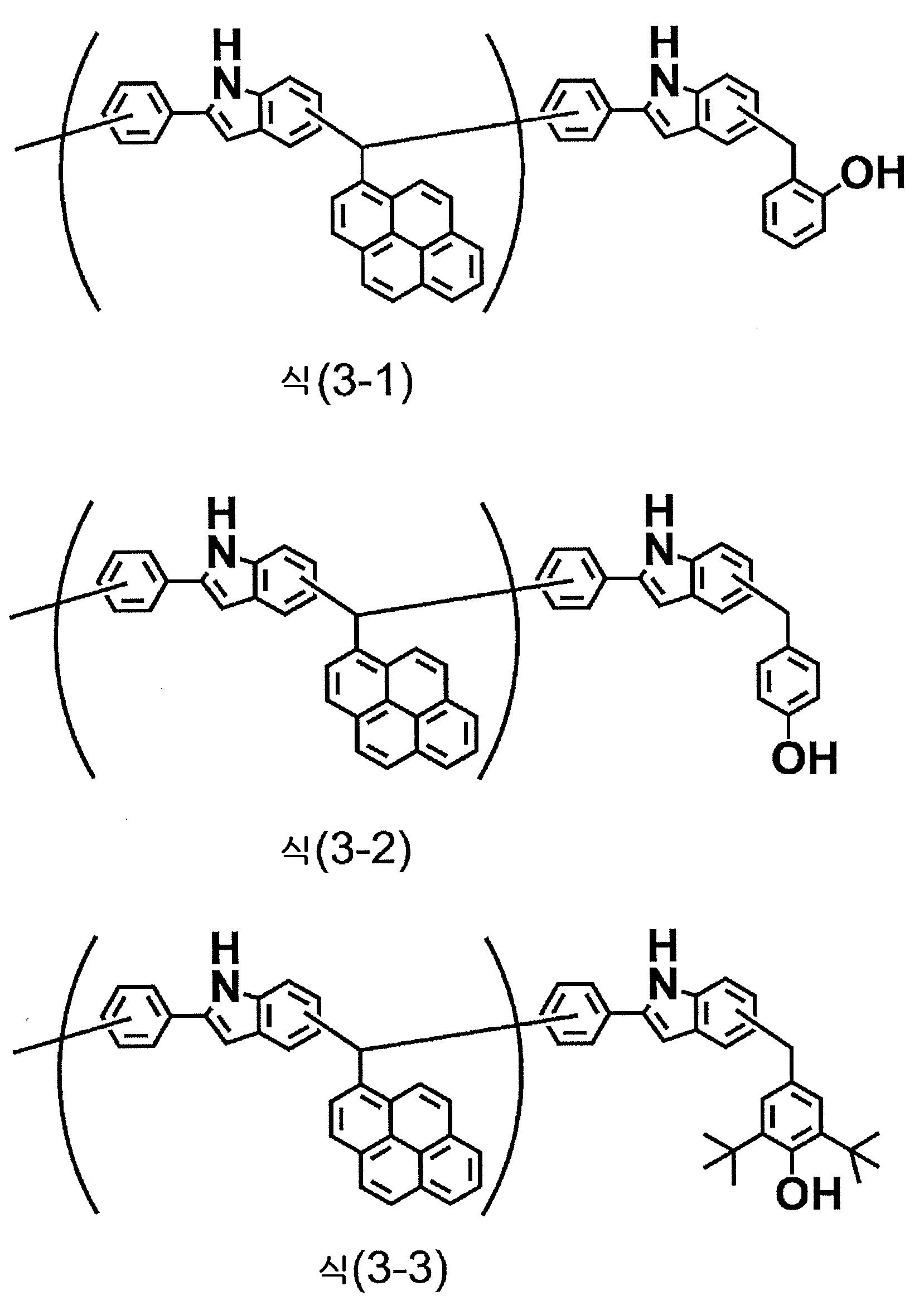
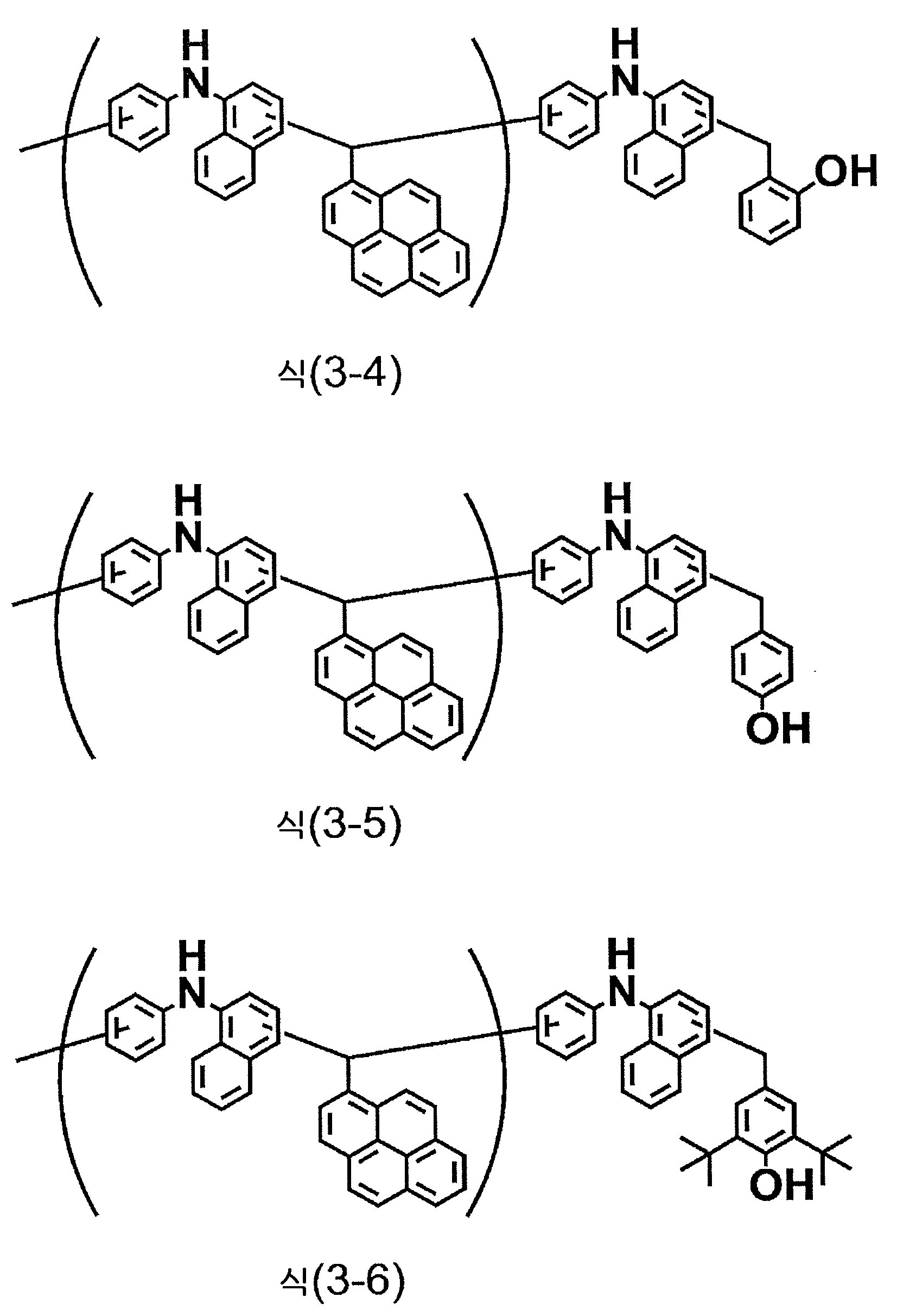
상기 방향족 아민이, 페닐인돌 또는 페닐나프틸아민인 레지스트 하층막 형성 조성물.
- 제7항에 있어서,
상기 페놀성 하이드록시기 함유 화합물이 페놀, 디하이드록시벤젠, 트리하이드록시벤젠, 하이드록시나프탈렌, 디하이드록시나프탈렌, 트리하이드록시나프탈렌, 트리스(4-하이드록시페닐)메탄, 트리스(4-하이드록시페닐)에탄, 또는 1,1,2,2-테트라키스(4-하이드록시페닐)에탄인 레지스트 하층막 형성 조성물.
- 제7항 내지 제9항 중 어느 한 항에 있어서,
상기 알데하이드가, 나프토알데하이드 또는 피렌카르복시알데하이드인 레지스트 하층막 형성 조성물.
- 제1항 내지 제10항 중 어느 한 항에 있어서,
용제를 추가로 포함하는 레지스트 하층막 형성 조성물.
- 제1항 내지 제11항 중 어느 한 항에 있어서,
산 및/또는 산발생제를 추가로 포함하는 레지스트 하층막 형성 조성물.
- 제1항 내지 제12항 중 어느 한 항에 있어서,
가교제를 추가로 포함하는 레지스트 하층막 형성 조성물.
- 제1항 내지 제13항 중 어느 한 항에 기재된 레지스트 하층막 형성 조성물을 반도체 기판 상에 도포하고, 소성하여 하층막을 형성하는 공정을 포함하는 반도체의 제조에 이용되는 레지스트 패턴의 형성방법.
- 반도체 기판 상에 제1항 내지 제13항 중 어느 한 항에 기재된 레지스트 하층막 형성 조성물에 의해 하층막을 형성하는 공정, 그 위에 레지스트막을 형성하는 공정, 광 또는 전자선의 조사와 현상에 의해 레지스트 패턴을 형성하는 공정, 이 레지스트 패턴에 의해 이 하층막을 에칭하는 공정, 및 패턴화된 하층막에 의해 반도체 기판을 가공하는 공정을 포함하는 반도체 장치의 제조방법.
- 반도체 기판 상에 제1항 내지 제13항 중 어느 한 항에 기재된 레지스트 하층막 형성 조성물에 의해 하층막을 형성하는 공정, 그 위에 하드마스크를 형성하는 공정, 다시 그 위에 레지스트막을 형성하는 공정, 광 또는 전자선의 조사와 현상에 의해 레지스트 패턴을 형성하는 공정, 이 레지스트 패턴에 의해 하드마스크를 에칭하는 공정, 패턴화된 하드마스크에 의해 이 하층막을 에칭하는 공정, 및 패턴화된 하층막에 의해 반도체 기판을 가공하는 공정을 포함하는 반도체 장치의 제조방법.
- 제16항에 있어서,
상기 하드마스크가 무기물의 증착막으로 이루어진 제조방법.
Applications Claiming Priority (3)
| Application Number | Priority Date | Filing Date | Title |
|---|---|---|---|
| JPJP-P-2014-162367 | 2014-08-08 | ||
| JP2014162367 | 2014-08-08 | ||
| PCT/JP2015/072081 WO2016021594A1 (ja) | 2014-08-08 | 2015-08-04 | 芳香族メチロール化合物が反応したノボラック樹脂を含むレジスト下層膜形成組成物 |
Publications (2)
| Publication Number | Publication Date |
|---|---|
| KR20170042500A true KR20170042500A (ko) | 2017-04-19 |
| KR102417838B1 KR102417838B1 (ko) | 2022-07-06 |
Family
ID=55263856
Family Applications (1)
| Application Number | Title | Priority Date | Filing Date |
|---|---|---|---|
| KR1020167032229A Active KR102417838B1 (ko) | 2014-08-08 | 2015-08-04 | 방향족 메틸올 화합물이 반응된 노볼락 수지를 포함하는 레지스트 하층막 형성 조성물 |
Country Status (6)
| Country | Link |
|---|---|
| US (1) | US11650505B2 (ko) |
| JP (1) | JP6703308B2 (ko) |
| KR (1) | KR102417838B1 (ko) |
| CN (1) | CN106662819B (ko) |
| TW (1) | TWI713462B (ko) |
| WO (1) | WO2016021594A1 (ko) |
Cited By (2)
| Publication number | Priority date | Publication date | Assignee | Title |
|---|---|---|---|---|
| US11214678B2 (en) | 2018-07-11 | 2022-01-04 | Samsung Sdi Co., Ltd. | Hardmask composition, hardmask layer and method of forming patterns |
| US11220570B2 (en) | 2018-12-26 | 2022-01-11 | Samsung Sdi Co., Ltd. | Polymer, hardmask composition, and method of forming patterns |
Families Citing this family (17)
| Publication number | Priority date | Publication date | Assignee | Title |
|---|---|---|---|---|
| WO2015151803A1 (ja) * | 2014-03-31 | 2015-10-08 | 日産化学工業株式会社 | 芳香族ビニル化合物が付加したノボラック樹脂を含むレジスト下層膜形成組成物 |
| KR101884447B1 (ko) * | 2015-07-06 | 2018-08-01 | 삼성에스디아이 주식회사 | 모노머, 유기막 조성물, 유기막, 및 패턴형성방법 |
| US20180356732A1 (en) | 2015-12-01 | 2018-12-13 | Nissan Chemical Industries, Ltd. | Resist underlayer film-forming composition containing indolocarbazole novolak resin |
| JP6643142B2 (ja) * | 2016-02-26 | 2020-02-12 | Hoya株式会社 | マスクブランク、レジスト膜付きマスクブランク、レジストパターン付きマスクブランク、およびそれらの製造方法、ならびに転写用マスクの製造方法 |
| KR102667884B1 (ko) * | 2016-07-27 | 2024-05-23 | 삼성전자주식회사 | 반도체 소자의 제조 방법 |
| KR102037818B1 (ko) * | 2016-11-10 | 2019-10-29 | 삼성에스디아이 주식회사 | 중합체, 유기막 조성물 및 패턴형성방법 |
| WO2018088673A1 (ko) * | 2016-11-10 | 2018-05-17 | 삼성에스디아이 주식회사 | 중합체, 유기막 조성물 및 패턴형성방법 |
| KR101940655B1 (ko) * | 2016-11-22 | 2019-01-21 | 동우 화인켐 주식회사 | 하드마스크용 조성물 |
| TWI748087B (zh) * | 2017-04-25 | 2021-12-01 | 日商日產化學工業股份有限公司 | 使用茀化合物之阻劑下層膜形成組成物 |
| JP6940335B2 (ja) * | 2017-08-30 | 2021-09-29 | 信越化学工業株式会社 | 有機膜形成用組成物、半導体装置製造用基板、有機膜の形成方法、パターン形成方法、及び重合体 |
| TWI801504B (zh) * | 2018-02-20 | 2023-05-11 | 日商日產化學股份有限公司 | 包含含有三芳基二胺之酚醛樹脂並加有芳香族乙烯基化合物的阻劑下層膜形成組成物 |
| KR102702755B1 (ko) * | 2018-07-20 | 2024-09-05 | 닛산 가가쿠 가부시키가이샤 | 레지스트 하층막 형성 조성물 |
| KR102539875B1 (ko) * | 2018-08-20 | 2023-06-05 | 동우 화인켐 주식회사 | 하드마스크용 조성물 |
| KR102260811B1 (ko) * | 2018-12-26 | 2021-06-03 | 삼성에스디아이 주식회사 | 하드마스크 조성물, 하드마스크 층 및 패턴 형성 방법 |
| US20210088901A1 (en) * | 2019-09-20 | 2021-03-25 | Imec Vzw | Photoresist for euv and/or e-beam lithography |
| JP7806692B2 (ja) * | 2020-06-19 | 2026-01-27 | 日産化学株式会社 | ジアリールメタン誘導体を用いたレジスト下層膜形成組成物 |
| CN120153321A (zh) * | 2022-11-02 | 2025-06-13 | 日产化学株式会社 | 抗蚀剂下层膜形成用组合物 |
Citations (11)
| Publication number | Priority date | Publication date | Assignee | Title |
|---|---|---|---|---|
| JPH01154050A (ja) | 1987-12-10 | 1989-06-16 | Toshiba Corp | パターン形成方法 |
| JPH0222657A (ja) | 1988-07-11 | 1990-01-25 | Hitachi Ltd | パターン形成方法および半導体装置製造方法 |
| JPH02293850A (ja) | 1989-05-09 | 1990-12-05 | Toshiba Corp | パターン形成方法 |
| JPH05204147A (ja) * | 1991-02-25 | 1993-08-13 | Sony Corp | 感光性樹脂組成物 |
| JP2005128509A (ja) | 2003-10-03 | 2005-05-19 | Shin Etsu Chem Co Ltd | フォトレジスト下層膜形成材料及びパターン形成方法 |
| JP2005156816A (ja) * | 2003-11-25 | 2005-06-16 | Tokyo Ohka Kogyo Co Ltd | 下地材及び多層レジストパターン形成方法 |
| JP2006259249A (ja) | 2005-03-17 | 2006-09-28 | Shin Etsu Chem Co Ltd | フォトレジスト下層膜形成材料及びパターン形成方法 |
| JP2007178974A (ja) | 2005-12-26 | 2007-07-12 | Cheil Industries Inc | フォトレジスト下層膜用ハードマスク組成物及びこれを利用した半導体集積回路デバイスの製造方法 |
| JP2007199653A (ja) | 2005-12-27 | 2007-08-09 | Shin Etsu Chem Co Ltd | フォトレジスト下層膜形成材料及びパターン形成方法 |
| WO2010147155A1 (ja) | 2009-06-19 | 2010-12-23 | 日産化学工業株式会社 | カルバゾールノボラック樹脂 |
| WO2013047516A1 (ja) * | 2011-09-29 | 2013-04-04 | 日産化学工業株式会社 | ジアリールアミンノボラック樹脂 |
Family Cites Families (26)
| Publication number | Priority date | Publication date | Assignee | Title |
|---|---|---|---|---|
| DE281918C (ko) * | ||||
| US2754335A (en) * | 1950-09-06 | 1956-07-10 | Union Carbide & Carbon Corp | Triphenylols |
| US2728741A (en) * | 1952-11-01 | 1955-12-27 | Lockheed Aircraft Corp | Phenol-formaldehyde resins for foaming compositions |
| DD281918A7 (de) * | 1982-12-04 | 1990-08-29 | Fotochem Werke Berlin Veb | Verfahren zur herstellung von novolaken mit weitgehend regelmaessigem molekuelaufbau |
| JPH01102457A (ja) * | 1987-10-15 | 1989-04-20 | Konica Corp | 感光性組成物 |
| JPH01289825A (ja) * | 1988-05-16 | 1989-11-21 | Fuji Photo Film Co Ltd | 高分子量ノボラック樹脂 |
| JP2734039B2 (ja) * | 1988-12-26 | 1998-03-30 | 住友化学工業株式会社 | ポジ型レジスト組成物 |
| US4939229A (en) * | 1989-05-12 | 1990-07-03 | Rohm And Haas Company | Method for preparing lithographically sensitive branched novolaks using a mannich base intermediate |
| TW338125B (en) * | 1993-02-26 | 1998-08-11 | Hoechst Celanese Corp | Novel matriz resin and its preparation and use in high-temperature stable photoimageable compositions |
| US5589553A (en) * | 1995-03-29 | 1996-12-31 | Shipley Company, L.L.C. | Esterification product of aromatic novolak resin with quinone diazide sulfonyl group |
| US5554719A (en) * | 1995-06-16 | 1996-09-10 | Hoechst Celanese Corporation | Polyhydroxystyrene with a novolak type structure |
| US5565544A (en) * | 1995-06-16 | 1996-10-15 | Hoechst Celanese Corporation | Process for preparing polyhydroxystyrene with a novolak type structure |
| JP3921705B2 (ja) * | 1996-05-31 | 2007-05-30 | 住友化学株式会社 | 多価フェノール系化合物およびその用途 |
| JP4252872B2 (ja) * | 2003-10-06 | 2009-04-08 | 信越化学工業株式会社 | レジスト下層膜材料およびパターン形成方法 |
| EP1739485B1 (en) * | 2004-04-15 | 2016-08-31 | Mitsubishi Gas Chemical Company, Inc. | Resist composition |
| KR100665758B1 (ko) | 2005-09-15 | 2007-01-09 | 제일모직주식회사 | 반사방지성을 갖는 하드마스크 조성물 |
| JP5018307B2 (ja) * | 2006-09-26 | 2012-09-05 | 富士通株式会社 | レジストパターン厚肉化材料、レジストパターンの形成方法、半導体装置及びその製造方法 |
| JP5485188B2 (ja) * | 2011-01-14 | 2014-05-07 | 信越化学工業株式会社 | レジスト下層膜材料及びこれを用いたパターン形成方法 |
| WO2012141165A1 (ja) * | 2011-04-12 | 2012-10-18 | Dic株式会社 | ポジ型フォトレジスト組成物、その塗膜及びノボラック型フェノール樹脂 |
| JP5859420B2 (ja) * | 2012-01-04 | 2016-02-10 | 信越化学工業株式会社 | レジスト下層膜材料、レジスト下層膜材料の製造方法、及び前記レジスト下層膜材料を用いたパターン形成方法 |
| WO2013146670A1 (ja) * | 2012-03-27 | 2013-10-03 | 日産化学工業株式会社 | フェニルインドール含有ノボラック樹脂を含むレジスト下層膜形成組成物 |
| JP5894106B2 (ja) * | 2012-06-18 | 2016-03-23 | 信越化学工業株式会社 | レジスト下層膜形成用化合物、これを用いたレジスト下層膜材料、レジスト下層膜形成方法、パターン形成方法 |
| CN104541205B (zh) * | 2012-08-21 | 2019-07-05 | 日产化学工业株式会社 | 含有具有多核苯酚的酚醛清漆树脂的抗蚀剂下层膜形成用组合物 |
| KR102200511B1 (ko) * | 2013-01-24 | 2021-01-11 | 닛산 가가쿠 가부시키가이샤 | 리소그래피용 레지스트 상층막 형성 조성물 및 이것을 이용한 반도체장치의 제조방법 |
| KR102229657B1 (ko) * | 2013-05-13 | 2021-03-18 | 닛산 가가쿠 가부시키가이샤 | 비스페놀알데히드를 이용한 노볼락 수지 함유 레지스트 하층막 형성 조성물 |
| WO2015151803A1 (ja) * | 2014-03-31 | 2015-10-08 | 日産化学工業株式会社 | 芳香族ビニル化合物が付加したノボラック樹脂を含むレジスト下層膜形成組成物 |
-
2015
- 2015-08-04 US US15/502,600 patent/US11650505B2/en active Active
- 2015-08-04 JP JP2016540245A patent/JP6703308B2/ja active Active
- 2015-08-04 KR KR1020167032229A patent/KR102417838B1/ko active Active
- 2015-08-04 WO PCT/JP2015/072081 patent/WO2016021594A1/ja not_active Ceased
- 2015-08-04 CN CN201580036571.3A patent/CN106662819B/zh active Active
- 2015-08-06 TW TW104125608A patent/TWI713462B/zh active
Patent Citations (11)
| Publication number | Priority date | Publication date | Assignee | Title |
|---|---|---|---|---|
| JPH01154050A (ja) | 1987-12-10 | 1989-06-16 | Toshiba Corp | パターン形成方法 |
| JPH0222657A (ja) | 1988-07-11 | 1990-01-25 | Hitachi Ltd | パターン形成方法および半導体装置製造方法 |
| JPH02293850A (ja) | 1989-05-09 | 1990-12-05 | Toshiba Corp | パターン形成方法 |
| JPH05204147A (ja) * | 1991-02-25 | 1993-08-13 | Sony Corp | 感光性樹脂組成物 |
| JP2005128509A (ja) | 2003-10-03 | 2005-05-19 | Shin Etsu Chem Co Ltd | フォトレジスト下層膜形成材料及びパターン形成方法 |
| JP2005156816A (ja) * | 2003-11-25 | 2005-06-16 | Tokyo Ohka Kogyo Co Ltd | 下地材及び多層レジストパターン形成方法 |
| JP2006259249A (ja) | 2005-03-17 | 2006-09-28 | Shin Etsu Chem Co Ltd | フォトレジスト下層膜形成材料及びパターン形成方法 |
| JP2007178974A (ja) | 2005-12-26 | 2007-07-12 | Cheil Industries Inc | フォトレジスト下層膜用ハードマスク組成物及びこれを利用した半導体集積回路デバイスの製造方法 |
| JP2007199653A (ja) | 2005-12-27 | 2007-08-09 | Shin Etsu Chem Co Ltd | フォトレジスト下層膜形成材料及びパターン形成方法 |
| WO2010147155A1 (ja) | 2009-06-19 | 2010-12-23 | 日産化学工業株式会社 | カルバゾールノボラック樹脂 |
| WO2013047516A1 (ja) * | 2011-09-29 | 2013-04-04 | 日産化学工業株式会社 | ジアリールアミンノボラック樹脂 |
Cited By (2)
| Publication number | Priority date | Publication date | Assignee | Title |
|---|---|---|---|---|
| US11214678B2 (en) | 2018-07-11 | 2022-01-04 | Samsung Sdi Co., Ltd. | Hardmask composition, hardmask layer and method of forming patterns |
| US11220570B2 (en) | 2018-12-26 | 2022-01-11 | Samsung Sdi Co., Ltd. | Polymer, hardmask composition, and method of forming patterns |
Also Published As
| Publication number | Publication date |
|---|---|
| WO2016021594A1 (ja) | 2016-02-11 |
| US11650505B2 (en) | 2023-05-16 |
| JP6703308B2 (ja) | 2020-06-03 |
| US20170227850A1 (en) | 2017-08-10 |
| KR102417838B1 (ko) | 2022-07-06 |
| JPWO2016021594A1 (ja) | 2017-05-25 |
| CN106662819B (zh) | 2021-06-25 |
| TWI713462B (zh) | 2020-12-21 |
| TW201620981A (zh) | 2016-06-16 |
| CN106662819A (zh) | 2017-05-10 |
Similar Documents
| Publication | Publication Date | Title |
|---|---|---|
| JP6703308B2 (ja) | 芳香族メチロール化合物が反応したノボラック樹脂を含むレジスト下層膜形成組成物 | |
| JP7208592B2 (ja) | 長鎖アルキル基含有ノボラックを含むレジスト下層膜形成組成物 | |
| JP6124025B2 (ja) | 多核フェノール類を有するノボラック樹脂を含むレジスト下層膜形成組成物 | |
| KR102367638B1 (ko) | 방향족 비닐화합물이 부가된 노볼락수지를 포함하는 레지스트 하층막 형성 조성물 | |
| KR102229657B1 (ko) | 비스페놀알데히드를 이용한 노볼락 수지 함유 레지스트 하층막 형성 조성물 | |
| JP6436313B2 (ja) | ピロールノボラック樹脂を含むレジスト下層膜形成組成物 | |
| TWI770055B (zh) | 含有含三芳基二胺之酚醛清漆樹脂的阻劑下層膜形成組成物 | |
| KR20140144207A (ko) | 페닐인돌 함유 노볼락 수지를 포함하는 레지스트 하층막 형성 조성물 | |
| KR20160102985A (ko) | 제2 아미노기를 갖는 노볼락폴리머를 포함하는 레지스트 하층막 형성 조성물 | |
| TW202346391A (zh) | 用以形成膜密度經提昇之阻劑下層膜的組成物 | |
| WO2023149553A1 (ja) | 焼成物の硬度の向上方法 |
Legal Events
| Date | Code | Title | Description |
|---|---|---|---|
| PA0105 | International application |
Patent event date: 20161118 Patent event code: PA01051R01D Comment text: International Patent Application |
|
| PG1501 | Laying open of application | ||
| A201 | Request for examination | ||
| PA0201 | Request for examination |
Patent event code: PA02012R01D Patent event date: 20200630 Comment text: Request for Examination of Application |
|
| E902 | Notification of reason for refusal | ||
| PE0902 | Notice of grounds for rejection |
Comment text: Notification of reason for refusal Patent event date: 20211202 Patent event code: PE09021S01D |
|
| E701 | Decision to grant or registration of patent right | ||
| PE0701 | Decision of registration |
Patent event code: PE07011S01D Comment text: Decision to Grant Registration Patent event date: 20220601 |
|
| GRNT | Written decision to grant | ||
| PR0701 | Registration of establishment |
Comment text: Registration of Establishment Patent event date: 20220701 Patent event code: PR07011E01D |
|
| PR1002 | Payment of registration fee |
Payment date: 20220704 End annual number: 3 Start annual number: 1 |
|
| PG1601 | Publication of registration |