KR20170050729A - 유기 발광 표시 장치 - Google Patents
유기 발광 표시 장치 Download PDFInfo
- Publication number
- KR20170050729A KR20170050729A KR1020150152619A KR20150152619A KR20170050729A KR 20170050729 A KR20170050729 A KR 20170050729A KR 1020150152619 A KR1020150152619 A KR 1020150152619A KR 20150152619 A KR20150152619 A KR 20150152619A KR 20170050729 A KR20170050729 A KR 20170050729A
- Authority
- KR
- South Korea
- Prior art keywords
- metal layer
- layer
- light emitting
- organic light
- electrode
- Prior art date
- Legal status (The legal status is an assumption and is not a legal conclusion. Google has not performed a legal analysis and makes no representation as to the accuracy of the status listed.)
- Ceased
Links
Images




Classifications
-
- H01L27/3262—
-
- H—ELECTRICITY
- H10—SEMICONDUCTOR DEVICES; ELECTRIC SOLID-STATE DEVICES NOT OTHERWISE PROVIDED FOR
- H10D—INORGANIC ELECTRIC SEMICONDUCTOR DEVICES
- H10D30/00—Field-effect transistors [FET]
- H10D30/60—Insulated-gate field-effect transistors [IGFET]
- H10D30/67—Thin-film transistors [TFT]
- H10D30/6729—Thin-film transistors [TFT] characterised by the electrodes
- H10D30/6737—Thin-film transistors [TFT] characterised by the electrodes characterised by the electrode materials
- H10D30/6739—Conductor-insulator-semiconductor electrodes
-
- H—ELECTRICITY
- H10—SEMICONDUCTOR DEVICES; ELECTRIC SOLID-STATE DEVICES NOT OTHERWISE PROVIDED FOR
- H10K—ORGANIC ELECTRIC SOLID-STATE DEVICES
- H10K59/00—Integrated devices, or assemblies of multiple devices, comprising at least one organic light-emitting element covered by group H10K50/00
- H10K59/10—OLED displays
- H10K59/12—Active-matrix OLED [AMOLED] displays
- H10K59/121—Active-matrix OLED [AMOLED] displays characterised by the geometry or disposition of pixel elements
- H10K59/1213—Active-matrix OLED [AMOLED] displays characterised by the geometry or disposition of pixel elements the pixel elements being TFTs
-
- H01L27/3246—
-
- H01L27/3248—
-
- H01L51/5212—
-
- H01L51/5215—
-
- H01L51/5218—
-
- H01L51/5228—
-
- H01L51/5231—
-
- H01L51/5234—
-
- H01L51/5284—
-
- H—ELECTRICITY
- H10—SEMICONDUCTOR DEVICES; ELECTRIC SOLID-STATE DEVICES NOT OTHERWISE PROVIDED FOR
- H10D—INORGANIC ELECTRIC SEMICONDUCTOR DEVICES
- H10D30/00—Field-effect transistors [FET]
- H10D30/60—Insulated-gate field-effect transistors [IGFET]
- H10D30/67—Thin-film transistors [TFT]
- H10D30/6729—Thin-film transistors [TFT] characterised by the electrodes
- H10D30/673—Thin-film transistors [TFT] characterised by the electrodes characterised by the shapes, relative sizes or dispositions of the gate electrodes
-
- H—ELECTRICITY
- H10—SEMICONDUCTOR DEVICES; ELECTRIC SOLID-STATE DEVICES NOT OTHERWISE PROVIDED FOR
- H10D—INORGANIC ELECTRIC SEMICONDUCTOR DEVICES
- H10D30/00—Field-effect transistors [FET]
- H10D30/60—Insulated-gate field-effect transistors [IGFET]
- H10D30/67—Thin-film transistors [TFT]
- H10D30/6729—Thin-film transistors [TFT] characterised by the electrodes
- H10D30/6737—Thin-film transistors [TFT] characterised by the electrodes characterised by the electrode materials
-
- H—ELECTRICITY
- H10—SEMICONDUCTOR DEVICES; ELECTRIC SOLID-STATE DEVICES NOT OTHERWISE PROVIDED FOR
- H10D—INORGANIC ELECTRIC SEMICONDUCTOR DEVICES
- H10D30/00—Field-effect transistors [FET]
- H10D30/60—Insulated-gate field-effect transistors [IGFET]
- H10D30/67—Thin-film transistors [TFT]
- H10D30/674—Thin-film transistors [TFT] characterised by the active materials
- H10D30/6741—Group IV materials, e.g. germanium or silicon carbide
- H10D30/6743—Silicon
-
- H—ELECTRICITY
- H10—SEMICONDUCTOR DEVICES; ELECTRIC SOLID-STATE DEVICES NOT OTHERWISE PROVIDED FOR
- H10D—INORGANIC ELECTRIC SEMICONDUCTOR DEVICES
- H10D30/00—Field-effect transistors [FET]
- H10D30/60—Insulated-gate field-effect transistors [IGFET]
- H10D30/67—Thin-film transistors [TFT]
- H10D30/6758—Thin-film transistors [TFT] characterised by the insulating substrates
-
- H—ELECTRICITY
- H10—SEMICONDUCTOR DEVICES; ELECTRIC SOLID-STATE DEVICES NOT OTHERWISE PROVIDED FOR
- H10D—INORGANIC ELECTRIC SEMICONDUCTOR DEVICES
- H10D64/00—Electrodes of devices having potential barriers
- H10D64/60—Electrodes characterised by their materials
-
- H—ELECTRICITY
- H10—SEMICONDUCTOR DEVICES; ELECTRIC SOLID-STATE DEVICES NOT OTHERWISE PROVIDED FOR
- H10D—INORGANIC ELECTRIC SEMICONDUCTOR DEVICES
- H10D86/00—Integrated devices formed in or on insulating or conducting substrates, e.g. formed in silicon-on-insulator [SOI] substrates or on stainless steel or glass substrates
- H10D86/40—Integrated devices formed in or on insulating or conducting substrates, e.g. formed in silicon-on-insulator [SOI] substrates or on stainless steel or glass substrates characterised by multiple TFTs
- H10D86/411—Integrated devices formed in or on insulating or conducting substrates, e.g. formed in silicon-on-insulator [SOI] substrates or on stainless steel or glass substrates characterised by multiple TFTs characterised by materials, geometry or structure of the substrates
-
- H—ELECTRICITY
- H10—SEMICONDUCTOR DEVICES; ELECTRIC SOLID-STATE DEVICES NOT OTHERWISE PROVIDED FOR
- H10D—INORGANIC ELECTRIC SEMICONDUCTOR DEVICES
- H10D86/00—Integrated devices formed in or on insulating or conducting substrates, e.g. formed in silicon-on-insulator [SOI] substrates or on stainless steel or glass substrates
- H10D86/40—Integrated devices formed in or on insulating or conducting substrates, e.g. formed in silicon-on-insulator [SOI] substrates or on stainless steel or glass substrates characterised by multiple TFTs
- H10D86/441—Interconnections, e.g. scanning lines
-
- H—ELECTRICITY
- H10—SEMICONDUCTOR DEVICES; ELECTRIC SOLID-STATE DEVICES NOT OTHERWISE PROVIDED FOR
- H10D—INORGANIC ELECTRIC SEMICONDUCTOR DEVICES
- H10D86/00—Integrated devices formed in or on insulating or conducting substrates, e.g. formed in silicon-on-insulator [SOI] substrates or on stainless steel or glass substrates
- H10D86/40—Integrated devices formed in or on insulating or conducting substrates, e.g. formed in silicon-on-insulator [SOI] substrates or on stainless steel or glass substrates characterised by multiple TFTs
- H10D86/60—Integrated devices formed in or on insulating or conducting substrates, e.g. formed in silicon-on-insulator [SOI] substrates or on stainless steel or glass substrates characterised by multiple TFTs wherein the TFTs are in active matrices
-
- H—ELECTRICITY
- H10—SEMICONDUCTOR DEVICES; ELECTRIC SOLID-STATE DEVICES NOT OTHERWISE PROVIDED FOR
- H10K—ORGANIC ELECTRIC SOLID-STATE DEVICES
- H10K10/00—Organic devices specially adapted for rectifying, amplifying, oscillating or switching; Organic capacitors or resistors having potential barriers
- H10K10/40—Organic transistors
- H10K10/46—Field-effect transistors, e.g. organic thin-film transistors [OTFT]
- H10K10/462—Insulated gate field-effect transistors [IGFETs]
- H10K10/481—Insulated gate field-effect transistors [IGFETs] characterised by the gate conductors
-
- H—ELECTRICITY
- H10—SEMICONDUCTOR DEVICES; ELECTRIC SOLID-STATE DEVICES NOT OTHERWISE PROVIDED FOR
- H10K—ORGANIC ELECTRIC SOLID-STATE DEVICES
- H10K10/00—Organic devices specially adapted for rectifying, amplifying, oscillating or switching; Organic capacitors or resistors having potential barriers
- H10K10/80—Constructional details
- H10K10/82—Electrodes
-
- H—ELECTRICITY
- H10—SEMICONDUCTOR DEVICES; ELECTRIC SOLID-STATE DEVICES NOT OTHERWISE PROVIDED FOR
- H10K—ORGANIC ELECTRIC SOLID-STATE DEVICES
- H10K10/00—Organic devices specially adapted for rectifying, amplifying, oscillating or switching; Organic capacitors or resistors having potential barriers
- H10K10/80—Constructional details
- H10K10/82—Electrodes
- H10K10/84—Ohmic electrodes, e.g. source or drain electrodes
-
- H—ELECTRICITY
- H10—SEMICONDUCTOR DEVICES; ELECTRIC SOLID-STATE DEVICES NOT OTHERWISE PROVIDED FOR
- H10K—ORGANIC ELECTRIC SOLID-STATE DEVICES
- H10K59/00—Integrated devices, or assemblies of multiple devices, comprising at least one organic light-emitting element covered by group H10K50/00
- H10K59/80—Constructional details
- H10K59/875—Arrangements for extracting light from the devices
- H10K59/878—Arrangements for extracting light from the devices comprising reflective means
-
- H01L2227/32—
-
- H—ELECTRICITY
- H10—SEMICONDUCTOR DEVICES; ELECTRIC SOLID-STATE DEVICES NOT OTHERWISE PROVIDED FOR
- H10K—ORGANIC ELECTRIC SOLID-STATE DEVICES
- H10K59/00—Integrated devices, or assemblies of multiple devices, comprising at least one organic light-emitting element covered by group H10K50/00
- H10K59/10—OLED displays
- H10K59/12—Active-matrix OLED [AMOLED] displays
Landscapes
- Physics & Mathematics (AREA)
- Geometry (AREA)
- Engineering & Computer Science (AREA)
- Microelectronics & Electronic Packaging (AREA)
- Electroluminescent Light Sources (AREA)
Abstract
본 발명의 실시예에 따른 유기 발광 표시 장치는 베이스 기판, 상기 베이스 기판의 상면에 배치된 버퍼층, 상기 버퍼층 상에 배치되며, 게이트 전극, 소스 전극, 및 드레인 전극을 포함하는 박막 트랜지스터, 및 상기 박막 트랜지스터와 연결되며 상기 박막 트랜지스터 상에 배치된 유기 발광 다이오드를 구비하고, 상기 게이트 전극, 소스 전극, 및 드레인 전극 중 적어도 어느 하나는 순차적으로 배치된 반투과 금속층, 투명 금속층, 및 반사 금속층을 포함한다.
Description
도 2는 본 발명의 실시예에 따른 유기 발광 표시 패널의 단면도.
도 3은 본 발명의 실시예에 따른 게이트 전극의 구조를 설명하기 위한 단면도.
도 4 및 도 5는 도 3에 도시된 제1 반사광 및 제2 반사광 간의 상쇄 간섭을 설명하기 위한 예시도.
도 6은 도 3에 도시된 투명 금속층의 두께에 따른 게이트 전극의 반사도를 나타낸 그래프.
도 7은 본 발명의 실시예에 따른 버퍼층의 구조를 설명하기 위한 단면도.
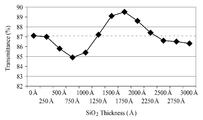
도 8은 도 7에 도시된 실리콘 산화막의 두께에 따른 버퍼층의 투과도를 나타낸 예시도.
도 9는 도 7에 도시된 실리콘 산화막의 두께에 따른 게이트 전극의 반사도를 나타낸 그래프.
도 10은 본 발명의 다른 실시예에 따른 유기 발광 표시 장치의 단면도.
도 11은 도 10에 도시된 하부 필름을 설명하기 위한 예시도.
도 12는 도 10에 도시된 하부 필름의 투과도에 따른 표시 패널의 반사도를 나타낸 그래프.
130 : 버퍼층 140 : 제2 버퍼층
180 : 봉지층 200 : 게이트 구동부
310 : 소스 드라이브 IC 330 : 연성필름
350 : 회로보드 400 : 타이밍 제어부
T : 박막 트랜지스터 DA : 표시 영역
GE : 게이트 전극 ML1 : 반투과 금속층
ML2 : 투명 금속층 ML3 : 반사 금속층
SE : 소스 전극 DE : 드레인 전극
Claims (11)
- 베이스 기판;
상기 베이스 기판의 상면에 배치된 버퍼층;
상기 버퍼층 상에 배치되며, 게이트 전극, 소스 전극, 및 드레인 전극을 포함하는 박막 트랜지스터; 및
상기 박막 트랜지스터와 연결되며, 상기 박막 트랜지스터 상에 배치된 유기 발광 다이오드를 구비하고,
상기 게이트 전극, 소스 전극, 및 드레인 전극 중 적어도 어느 하나는 순차적으로 배치된 반투과 금속층, 투명 금속층, 및 반사 금속층을 포함하는 유기 발광 표시 장치. - 제 1 항에 있어서,
상기 반투과 금속층의 두께가 가장 얇고, 상기 반사 금속층의 두께가 가장 두꺼운 유기 발광 표시 장치. - 제 1 항에 있어서,
상기 반사 금속층은 상기 반투과 금속층보다 더 많은 광을 반사시키는 유기 발광 표시 장치. - 제 1 항에 있어서,
상기 투명 금속층의 두께는 350Å 내지 450Å 범위인 유기 발광 표시 장치. - 제 1 항에 있어서,
상기 베이스 기판은 10ppm/℃ 이하의 열팽창 계수를 갖는 폴리이미드(PI) 필름인 유기 발광 표시 장치. - 제 1 항에 있어서,
상기 베이스 기판의 하면에 배치된 하부 필름을 더 포함하고,
상기 하부 필름은 광을 흡수하는 물질을 포함하는 유기 발광 표시 장치. - 제 6 항에 있어서,
상기 하부 필름은 80% 내지 50%의 투과도를 갖는 유기 발광 표시 장치. - 제 1 항에 있어서,
상기 버퍼층은,
상기 베이스 기판 상에 마련된 제1 버퍼층; 및
상기 제1 버퍼층 상에 마련된 제2 버퍼층을 구비하고,
상기 제1 버퍼층은 실리콘 산화막 및 실리콘 질화막을 포함하는 유기 발광 표시 장치. - 제 8 항에 있어서,
상기 실리콘 산화막의 두께는 상기 실리콘 질화막의 두께와 동일하거나, 두꺼운 유기 발광 표시 장치. - 제 8 항에 있어서,
상기 실리콘 산화막의 두께는 1500Å 내지 2000Å 범위인 유기 발광 표시 장치. - 제 1 항에 있어서,
상기 유기발광 다이오드는,
상기 드레인 전극에 접속된 애노드 전극;
상기 애노드 전극을 구획하는 뱅크;
상기 애노드 전극 상에 마련된 유기 발광층; 및
상기 유기 발광층 상에 마련된 캐소드 전극을 더 구비하고,
상기 뱅크는 광을 흡수하는 물질을 포함하는 유기 발광 표시 장치.
Priority Applications (4)
| Application Number | Priority Date | Filing Date | Title |
|---|---|---|---|
| KR1020150152619A KR20170050729A (ko) | 2015-10-30 | 2015-10-30 | 유기 발광 표시 장치 |
| CN201610799430.3A CN106653797B (zh) | 2015-10-30 | 2016-08-31 | 有机发光显示装置 |
| US15/254,122 US10103210B2 (en) | 2015-10-30 | 2016-09-01 | Organic light emitting display device |
| EP16196443.2A EP3163621B1 (en) | 2015-10-30 | 2016-10-28 | Organic light emitting display device |
Applications Claiming Priority (1)
| Application Number | Priority Date | Filing Date | Title |
|---|---|---|---|
| KR1020150152619A KR20170050729A (ko) | 2015-10-30 | 2015-10-30 | 유기 발광 표시 장치 |
Publications (1)
| Publication Number | Publication Date |
|---|---|
| KR20170050729A true KR20170050729A (ko) | 2017-05-11 |
Family
ID=57326171
Family Applications (1)
| Application Number | Title | Priority Date | Filing Date |
|---|---|---|---|
| KR1020150152619A Ceased KR20170050729A (ko) | 2015-10-30 | 2015-10-30 | 유기 발광 표시 장치 |
Country Status (4)
| Country | Link |
|---|---|
| US (1) | US10103210B2 (ko) |
| EP (1) | EP3163621B1 (ko) |
| KR (1) | KR20170050729A (ko) |
| CN (1) | CN106653797B (ko) |
Cited By (2)
| Publication number | Priority date | Publication date | Assignee | Title |
|---|---|---|---|---|
| KR20210098955A (ko) * | 2018-12-05 | 2021-08-11 | 도판 인사츠 가부시키가이샤 | 블랙 매트릭스 기판, 및 블랙 매트릭스 기판을 구비한 표시 장치 |
| US12471454B2 (en) | 2020-11-26 | 2025-11-11 | Samsung Display Co., Ltd. | Display device and method of manufacturing the same |
Families Citing this family (12)
| Publication number | Priority date | Publication date | Assignee | Title |
|---|---|---|---|---|
| KR20170050729A (ko) * | 2015-10-30 | 2017-05-11 | 엘지디스플레이 주식회사 | 유기 발광 표시 장치 |
| KR102519678B1 (ko) * | 2016-08-01 | 2023-04-07 | 삼성디스플레이 주식회사 | 유기 발광 표시 장치 |
| KR102355103B1 (ko) * | 2017-09-29 | 2022-01-24 | 엘지디스플레이 주식회사 | 플렉서블 표시장치 및 그의 제조방법 |
| CN108766978B (zh) * | 2018-05-24 | 2020-02-21 | 京东方科技集团股份有限公司 | Oled显示基板及其制作方法、显示装置 |
| CN110767660B (zh) | 2018-07-24 | 2022-09-16 | 京东方科技集团股份有限公司 | 阵列基板及其制备方法、显示面板 |
| US11022853B2 (en) * | 2018-08-24 | 2021-06-01 | Sharp Kabushiki Kaisha | Display panel |
| CN110858035B (zh) * | 2018-08-24 | 2022-12-02 | 夏普株式会社 | 液晶显示装置 |
| KR102786529B1 (ko) * | 2018-12-31 | 2025-03-27 | 엘지디스플레이 주식회사 | 투명 표시 장치 |
| CN110164942A (zh) * | 2019-05-31 | 2019-08-23 | 江苏集萃有机光电技术研究所有限公司 | 一种显示面板及其制备方法、显示装置 |
| CN111430428B (zh) * | 2020-04-10 | 2023-02-07 | 京东方科技集团股份有限公司 | 柔性显示面板及其制作方法、显示装置 |
| CN112447785B (zh) * | 2020-11-23 | 2022-09-23 | 厦门天马微电子有限公司 | 一种发光二极管显示面板及其制备方法、显示装置 |
| US12471441B2 (en) * | 2021-11-02 | 2025-11-11 | Lg Display Co., Ltd. | Electroluminescence display |
Family Cites Families (65)
| Publication number | Priority date | Publication date | Assignee | Title |
|---|---|---|---|---|
| KR20070001169A (ko) * | 2004-03-05 | 2007-01-03 | 이데미쓰 고산 가부시키가이샤 | 반투명ㆍ반사 전극 기판, 그의 제조 방법, 및 이러한반투과ㆍ반반사 전극 기판을 이용한 액정 표시 장치 |
| KR100601374B1 (ko) * | 2004-05-28 | 2006-07-13 | 삼성에스디아이 주식회사 | 박막 트랜지스터 및 그 제조방법과 박막 트랜지스터를포함하는 평판표시장치 |
| TW200738765A (en) * | 2006-03-23 | 2007-10-16 | Zeon Corp | Norbornene compound addition polymer film, process for production thereof, and use thereof |
| KR100759681B1 (ko) * | 2006-03-29 | 2007-09-17 | 삼성에스디아이 주식회사 | 유기 전계 발광표시장치 |
| KR100769444B1 (ko) * | 2006-06-09 | 2007-10-22 | 삼성에스디아이 주식회사 | 유기 전계 발광표시장치 |
| US7919795B2 (en) * | 2006-12-21 | 2011-04-05 | Samsung Electronics Co., Ltd. | Wire structure, method for fabricating wire, thin film transistor substrate, and method for fabricating the thin film transistor substrate |
| KR100788551B1 (ko) * | 2006-12-29 | 2007-12-26 | 삼성에스디아이 주식회사 | 유기 전계 발광 표시 장치 및 그 제조 방법 |
| KR100859657B1 (ko) * | 2007-01-08 | 2008-09-23 | 삼성에스디아이 주식회사 | 솔라 셀을 구비한 유기 전계 발광 표시 장치 |
| US8227808B2 (en) * | 2007-12-06 | 2012-07-24 | Chimei Innolux Corporation | Method for manufacturing thin film transistor (TFT) and OLED display having TFTS manufactured by the same |
| CN103972246B (zh) * | 2009-07-27 | 2017-05-31 | 株式会社神户制钢所 | 布线结构以及具备布线结构的显示装置 |
| KR101084181B1 (ko) * | 2010-01-05 | 2011-11-17 | 삼성모바일디스플레이주식회사 | 유기 발광 표시 장치 |
| US9013461B2 (en) * | 2010-03-18 | 2015-04-21 | Samsung Display Co., Ltd. | Organic light emitting diode display |
| KR101692954B1 (ko) * | 2010-05-17 | 2017-01-05 | 삼성디스플레이 주식회사 | 유기 발광 디스플레이 장치 및 그 제조 방법 |
| KR101676313B1 (ko) * | 2010-05-31 | 2016-11-16 | 삼성디스플레이 주식회사 | 유기 발광 장치 |
| KR101716471B1 (ko) * | 2010-06-07 | 2017-03-28 | 삼성디스플레이 주식회사 | 유기 발광 표시 장치 및 그 제조 방법 |
| KR101234230B1 (ko) * | 2010-06-17 | 2013-02-18 | 삼성디스플레이 주식회사 | 유기 발광 디스플레이 장치 및 그 제조 방법 |
| KR101705822B1 (ko) | 2010-10-27 | 2017-02-23 | 삼성디스플레이 주식회사 | 유기 발광 표시 장치 및 그 제조 방법 |
| KR101727668B1 (ko) * | 2010-10-28 | 2017-04-18 | 삼성디스플레이 주식회사 | 유기 발광 표시 장치 |
| KR101822563B1 (ko) * | 2010-12-08 | 2018-03-09 | 삼성디스플레이 주식회사 | 유기 발광 표시 장치 및 그 제조 방법 |
| KR101223487B1 (ko) | 2010-12-30 | 2013-01-17 | 삼성디스플레이 주식회사 | 투명 전극, 상기 투명 전극을 포함하는 유기 발광 장치 및 그 제조 방법 |
| JP5171990B2 (ja) * | 2011-05-13 | 2013-03-27 | 株式会社神戸製鋼所 | Cu合金膜および表示装置 |
| KR20120139386A (ko) | 2011-06-17 | 2012-12-27 | 삼성디스플레이 주식회사 | 유기 발광 표시 장치 |
| KR101893355B1 (ko) * | 2011-06-30 | 2018-10-05 | 삼성디스플레이 주식회사 | 발광 소자 및 이를 포함하는 유기 발광 표시 장치 |
| WO2013073301A1 (ja) * | 2011-11-14 | 2013-05-23 | コニカミノルタ株式会社 | 有機エレクトロルミネッセンス素子、及び、面状発光体 |
| KR101912923B1 (ko) * | 2011-12-12 | 2018-10-30 | 삼성디스플레이 주식회사 | 유기 발광 표시 장치 및 그 제조 방법 |
| KR102068956B1 (ko) * | 2012-02-15 | 2020-01-23 | 엘지디스플레이 주식회사 | 박막트랜지스터, 박막트랜지스터 어레이 기판 및 이의 제조방법 |
| KR20140031003A (ko) * | 2012-09-04 | 2014-03-12 | 삼성디스플레이 주식회사 | 유기 발광 표시 장치 및 그 제조 방법 |
| KR101975957B1 (ko) * | 2012-10-04 | 2019-05-08 | 삼성디스플레이 주식회사 | 유기 발광 표시 장치 |
| KR101978783B1 (ko) * | 2012-11-09 | 2019-05-15 | 엘지디스플레이 주식회사 | 플렉서블 유기전계발광소자 및 그 제조방법 |
| KR101980757B1 (ko) * | 2012-12-13 | 2019-05-21 | 엘지디스플레이 주식회사 | 유기발광 표시장치 |
| KR102222680B1 (ko) * | 2013-02-01 | 2021-03-03 | 엘지디스플레이 주식회사 | 플렉서블 디스플레이 기판, 플렉서블 유기 발광 표시 장치 및 플렉서블 유기 발광 표시 장치 제조 방법 |
| KR102028680B1 (ko) * | 2013-03-20 | 2019-11-05 | 삼성디스플레이 주식회사 | 유기 발광 표시 장치 |
| KR102028988B1 (ko) * | 2013-04-02 | 2019-10-07 | 엘지디스플레이 주식회사 | 액정표시장치 및 그 제조방법 |
| KR102076666B1 (ko) * | 2013-04-11 | 2020-02-12 | 엘지디스플레이 주식회사 | 플렉서블 표시패널 |
| KR102018733B1 (ko) * | 2013-06-13 | 2019-09-06 | 삼성디스플레이 주식회사 | 플렉서블 표시장치 |
| JP6299478B2 (ja) * | 2013-06-26 | 2018-03-28 | 日亜化学工業株式会社 | 発光装置およびその製造方法 |
| US9257672B2 (en) * | 2013-09-09 | 2016-02-09 | Samsung Display Co., Ltd. | Organic light-emitting display apparatus |
| KR102188029B1 (ko) * | 2013-09-24 | 2020-12-08 | 삼성디스플레이 주식회사 | 유기 발광 표시 장치 및 유기 발광 장치의 제조 방법 |
| US20150140321A1 (en) * | 2013-11-15 | 2015-05-21 | Alliance For Sustainable Energy, Llc | Methodology for improved adhesion for deposited fluorinated transparent conducting oxide films on a substrate |
| KR102086805B1 (ko) * | 2013-11-19 | 2020-03-09 | 엘지디스플레이 주식회사 | 유기전계발광표시장치 |
| KR102112979B1 (ko) * | 2013-11-20 | 2020-05-20 | 엘지디스플레이 주식회사 | 액정표시장치 및 그 제조방법 |
| KR102162912B1 (ko) * | 2013-12-06 | 2020-10-07 | 엘지디스플레이 주식회사 | 터치패널을 구비한 유기전계 발광장치 및 그 제조방법 |
| KR102181238B1 (ko) * | 2014-02-12 | 2020-11-23 | 삼성디스플레이 주식회사 | 유기 발광 표시 장치 및 유기 발광 표시 장치의 제조 방법 |
| KR102256083B1 (ko) * | 2014-03-26 | 2021-05-26 | 엘지디스플레이 주식회사 | 유기전계발광표시장치 |
| EP2963687B1 (en) * | 2014-07-03 | 2020-03-18 | LG Display Co., Ltd. | Organic electroluminescent device |
| KR102364387B1 (ko) * | 2014-07-04 | 2022-02-18 | 삼성디스플레이 주식회사 | 유기 발광 표시 장치 |
| KR102245722B1 (ko) * | 2014-08-05 | 2021-04-29 | 삼성디스플레이 주식회사 | 유기 발광 표시 장치 및 유기 발광 표시 장치의 제조 방법 |
| CN104143533B (zh) * | 2014-08-07 | 2017-06-27 | 深圳市华星光电技术有限公司 | 高解析度amoled背板制造方法 |
| KR102148857B1 (ko) * | 2014-08-14 | 2020-08-28 | 삼성디스플레이 주식회사 | 표시장치 및 그 제조 방법 |
| KR102251840B1 (ko) * | 2014-08-14 | 2021-05-13 | 엘지디스플레이 주식회사 | 저반사 패널을 포함하는 유기발광 표시장치 |
| KR102230943B1 (ko) * | 2014-08-14 | 2021-03-24 | 엘지디스플레이 주식회사 | 광흡수층을 포함하는 유기발광 표시장치 및 이를 제조하는 방법 |
| KR102310902B1 (ko) * | 2014-09-15 | 2021-10-12 | 삼성디스플레이 주식회사 | 유기발광 디스플레이 장치 및 그 제조방법 |
| CN105575993B (zh) * | 2014-10-15 | 2018-07-24 | 上海和辉光电有限公司 | 有机发光显示装置及其制作方法 |
| US9627463B2 (en) * | 2014-11-28 | 2017-04-18 | Lg Display Co., Ltd. | Flexible display device with space reducing wire configuration |
| CN104485351A (zh) * | 2014-12-31 | 2015-04-01 | 深圳市华星光电技术有限公司 | 一种柔性有机发光显示器及其制作方法 |
| KR102348725B1 (ko) * | 2015-04-30 | 2022-01-07 | 엘지디스플레이 주식회사 | 플렉서블 디스플레이 장치 및 이의 제조 방법 |
| KR102348353B1 (ko) * | 2015-04-30 | 2022-01-07 | 엘지디스플레이 주식회사 | 플렉서블 디스플레이 장치 및 이의 제조 방법 |
| KR102554963B1 (ko) * | 2015-10-29 | 2023-07-11 | 엘지디스플레이 주식회사 | 유기 발광 표시 장치 |
| KR20170050729A (ko) * | 2015-10-30 | 2017-05-11 | 엘지디스플레이 주식회사 | 유기 발광 표시 장치 |
| KR102665737B1 (ko) * | 2015-12-09 | 2024-05-10 | 엘지디스플레이 주식회사 | 반사형 표시장치 |
| KR102492454B1 (ko) * | 2015-12-11 | 2023-01-27 | 엘지디스플레이 주식회사 | 폴더블 표시 장치 |
| US9793334B2 (en) * | 2015-12-31 | 2017-10-17 | Lg Display Co., Ltd. | Electronic device with flexible display panel including polarization layer with undercut portion and micro-coating layer |
| KR102483229B1 (ko) * | 2015-12-31 | 2022-12-29 | 엘지디스플레이 주식회사 | 유기발광 표시장치 |
| CN107808892B (zh) * | 2016-09-08 | 2020-06-26 | 群创光电股份有限公司 | 显示设备 |
| KR102627305B1 (ko) * | 2016-12-30 | 2024-01-18 | 한양대학교 산학협력단 | 박막 트랜지스터 기판 및 표시 장치 |
-
2015
- 2015-10-30 KR KR1020150152619A patent/KR20170050729A/ko not_active Ceased
-
2016
- 2016-08-31 CN CN201610799430.3A patent/CN106653797B/zh active Active
- 2016-09-01 US US15/254,122 patent/US10103210B2/en active Active
- 2016-10-28 EP EP16196443.2A patent/EP3163621B1/en active Active
Cited By (2)
| Publication number | Priority date | Publication date | Assignee | Title |
|---|---|---|---|---|
| KR20210098955A (ko) * | 2018-12-05 | 2021-08-11 | 도판 인사츠 가부시키가이샤 | 블랙 매트릭스 기판, 및 블랙 매트릭스 기판을 구비한 표시 장치 |
| US12471454B2 (en) | 2020-11-26 | 2025-11-11 | Samsung Display Co., Ltd. | Display device and method of manufacturing the same |
Also Published As
| Publication number | Publication date |
|---|---|
| EP3163621B1 (en) | 2020-01-15 |
| CN106653797A (zh) | 2017-05-10 |
| US10103210B2 (en) | 2018-10-16 |
| EP3163621A1 (en) | 2017-05-03 |
| US20170125492A1 (en) | 2017-05-04 |
| CN106653797B (zh) | 2019-11-15 |
Similar Documents
| Publication | Publication Date | Title |
|---|---|---|
| KR20170050729A (ko) | 유기 발광 표시 장치 | |
| US10910441B2 (en) | Organic light emitting display device | |
| US10319951B2 (en) | Organic light-emitting display device and method for manufacturing the same | |
| KR102424597B1 (ko) | 플렉서블 유기발광다이오드 표시장치 및 그 제조 방법 | |
| KR20190048642A (ko) | 디스플레이 장치 | |
| KR20180032719A (ko) | 표시 장치 | |
| KR102555648B1 (ko) | 표시장치 | |
| US12389784B2 (en) | Touch display device for blocking the penetration of moisture into the interior while extending the cathode electrode | |
| KR102375894B1 (ko) | 표시 장치 및 그 제조 방법 | |
| WO2019167279A1 (ja) | 表示装置 | |
| KR20190071295A (ko) | 유기 발광 표시 장치 | |
| WO2019064591A1 (ja) | 表示デバイス、表示デバイスの製造方法 | |
| US11723243B2 (en) | Organic light emitting display device including a connecting structure with dummy pad on flexible substrate | |
| KR20200025582A (ko) | 표시장치 | |
| WO2019167174A1 (ja) | 表示装置 | |
| US20240260438A1 (en) | Display Device | |
| US20240206287A1 (en) | Display device | |
| US20220320457A1 (en) | Display device | |
| KR20180061843A (ko) | 유기발광 표시장치 | |
| JP7451644B2 (ja) | 表示装置 | |
| KR102392326B1 (ko) | 유기 발광 표시 장치 | |
| KR20170079927A (ko) | 유기 발광 표시 장치 | |
| CN118742102A (zh) | 有机发光显示装置 | |
| KR102466445B1 (ko) | 유기 발광 표시 장치 | |
| KR20170080140A (ko) | 플렉서블 표시장치 및 그의 제조방법 |
Legal Events
| Date | Code | Title | Description |
|---|---|---|---|
| PA0109 | Patent application |
St.27 status event code: A-0-1-A10-A12-nap-PA0109 |
|
| PG1501 | Laying open of application |
St.27 status event code: A-1-1-Q10-Q12-nap-PG1501 |
|
| P11-X000 | Amendment of application requested |
St.27 status event code: A-2-2-P10-P11-nap-X000 |
|
| P13-X000 | Application amended |
St.27 status event code: A-2-2-P10-P13-nap-X000 |
|
| P22-X000 | Classification modified |
St.27 status event code: A-2-2-P10-P22-nap-X000 |
|
| A201 | Request for examination | ||
| PA0201 | Request for examination |
St.27 status event code: A-1-2-D10-D11-exm-PA0201 |
|
| E902 | Notification of reason for refusal | ||
| PE0902 | Notice of grounds for rejection |
St.27 status event code: A-1-2-D10-D21-exm-PE0902 |
|
| E13-X000 | Pre-grant limitation requested |
St.27 status event code: A-2-3-E10-E13-lim-X000 |
|
| P11-X000 | Amendment of application requested |
St.27 status event code: A-2-2-P10-P11-nap-X000 |
|
| P13-X000 | Application amended |
St.27 status event code: A-2-2-P10-P13-nap-X000 |
|
| E601 | Decision to refuse application | ||
| PE0601 | Decision on rejection of patent |
St.27 status event code: N-2-6-B10-B15-exm-PE0601 |
|
| P22-X000 | Classification modified |
St.27 status event code: A-2-2-P10-P22-nap-X000 |
|
| P22-X000 | Classification modified |
St.27 status event code: A-2-2-P10-P22-nap-X000 |
|
| P22-X000 | Classification modified |
St.27 status event code: A-2-2-P10-P22-nap-X000 |
|
| P22-X000 | Classification modified |
St.27 status event code: A-2-2-P10-P22-nap-X000 |