KR20170051794A - Display Device And Driving Method Of The Same - Google Patents
Display Device And Driving Method Of The Same Download PDFInfo
- Publication number
- KR20170051794A KR20170051794A KR1020150152679A KR20150152679A KR20170051794A KR 20170051794 A KR20170051794 A KR 20170051794A KR 1020150152679 A KR1020150152679 A KR 1020150152679A KR 20150152679 A KR20150152679 A KR 20150152679A KR 20170051794 A KR20170051794 A KR 20170051794A
- Authority
- KR
- South Korea
- Prior art keywords
- sensor
- input
- data
- sensing area
- fingerprint
- Prior art date
- Legal status (The legal status is an assumption and is not a legal conclusion. Google has not performed a legal analysis and makes no representation as to the accuracy of the status listed.)
- Granted
Links
Images




Classifications
-
- G—PHYSICS
- G09—EDUCATION; CRYPTOGRAPHY; DISPLAY; ADVERTISING; SEALS
- G09G—ARRANGEMENTS OR CIRCUITS FOR CONTROL OF INDICATING DEVICES USING STATIC MEANS TO PRESENT VARIABLE INFORMATION
- G09G3/00—Control arrangements or circuits, of interest only in connection with visual indicators other than cathode-ray tubes
- G09G3/20—Control arrangements or circuits, of interest only in connection with visual indicators other than cathode-ray tubes for presentation of an assembly of a number of characters, e.g. a page, by composing the assembly by combination of individual elements arranged in a matrix no fixed position being assigned to or needed to be assigned to the individual characters or partial characters
-
- G—PHYSICS
- G06—COMPUTING OR CALCULATING; COUNTING
- G06F—ELECTRIC DIGITAL DATA PROCESSING
- G06F3/00—Input arrangements for transferring data to be processed into a form capable of being handled by the computer; Output arrangements for transferring data from processing unit to output unit, e.g. interface arrangements
- G06F3/01—Input arrangements or combined input and output arrangements for interaction between user and computer
- G06F3/03—Arrangements for converting the position or the displacement of a member into a coded form
- G06F3/041—Digitisers, e.g. for touch screens or touch pads, characterised by the transducing means
- G06F3/0412—Digitisers structurally integrated in a display
-
- G—PHYSICS
- G06—COMPUTING OR CALCULATING; COUNTING
- G06F—ELECTRIC DIGITAL DATA PROCESSING
- G06F3/00—Input arrangements for transferring data to be processed into a form capable of being handled by the computer; Output arrangements for transferring data from processing unit to output unit, e.g. interface arrangements
- G06F3/01—Input arrangements or combined input and output arrangements for interaction between user and computer
- G06F3/03—Arrangements for converting the position or the displacement of a member into a coded form
- G06F3/041—Digitisers, e.g. for touch screens or touch pads, characterised by the transducing means
- G06F3/0416—Control or interface arrangements specially adapted for digitisers
-
- G—PHYSICS
- G06—COMPUTING OR CALCULATING; COUNTING
- G06F—ELECTRIC DIGITAL DATA PROCESSING
- G06F3/00—Input arrangements for transferring data to be processed into a form capable of being handled by the computer; Output arrangements for transferring data from processing unit to output unit, e.g. interface arrangements
- G06F3/01—Input arrangements or combined input and output arrangements for interaction between user and computer
- G06F3/03—Arrangements for converting the position or the displacement of a member into a coded form
- G06F3/041—Digitisers, e.g. for touch screens or touch pads, characterised by the transducing means
- G06F3/044—Digitisers, e.g. for touch screens or touch pads, characterised by the transducing means by capacitive means
-
- G06K9/00006—
-
- G—PHYSICS
- G09—EDUCATION; CRYPTOGRAPHY; DISPLAY; ADVERTISING; SEALS
- G09G—ARRANGEMENTS OR CIRCUITS FOR CONTROL OF INDICATING DEVICES USING STATIC MEANS TO PRESENT VARIABLE INFORMATION
- G09G3/00—Control arrangements or circuits, of interest only in connection with visual indicators other than cathode-ray tubes
- G09G3/20—Control arrangements or circuits, of interest only in connection with visual indicators other than cathode-ray tubes for presentation of an assembly of a number of characters, e.g. a page, by composing the assembly by combination of individual elements arranged in a matrix no fixed position being assigned to or needed to be assigned to the individual characters or partial characters
- G09G3/34—Control arrangements or circuits, of interest only in connection with visual indicators other than cathode-ray tubes for presentation of an assembly of a number of characters, e.g. a page, by composing the assembly by combination of individual elements arranged in a matrix no fixed position being assigned to or needed to be assigned to the individual characters or partial characters by control of light from an independent source
- G09G3/36—Control arrangements or circuits, of interest only in connection with visual indicators other than cathode-ray tubes for presentation of an assembly of a number of characters, e.g. a page, by composing the assembly by combination of individual elements arranged in a matrix no fixed position being assigned to or needed to be assigned to the individual characters or partial characters by control of light from an independent source using liquid crystals
- G09G3/3611—Control of matrices with row and column drivers
- G09G3/3648—Control of matrices with row and column drivers using an active matrix
-
- G—PHYSICS
- G09—EDUCATION; CRYPTOGRAPHY; DISPLAY; ADVERTISING; SEALS
- G09G—ARRANGEMENTS OR CIRCUITS FOR CONTROL OF INDICATING DEVICES USING STATIC MEANS TO PRESENT VARIABLE INFORMATION
- G09G2310/00—Command of the display device
- G09G2310/08—Details of timing specific for flat panels, other than clock recovery
Landscapes
- Engineering & Computer Science (AREA)
- Theoretical Computer Science (AREA)
- General Engineering & Computer Science (AREA)
- Physics & Mathematics (AREA)
- General Physics & Mathematics (AREA)
- Human Computer Interaction (AREA)
- Computer Hardware Design (AREA)
- Chemical & Material Sciences (AREA)
- Crystallography & Structural Chemistry (AREA)
- Image Input (AREA)
- Liquid Crystal Display Device Control (AREA)
- Liquid Crystal (AREA)
- Control Of Indicators Other Than Cathode Ray Tubes (AREA)
Abstract
Description
본 발명은 터치 입력과 지문 입력을 센싱할 수 있는 표시 장치와 그 구동방법에 관한 것이다.The present invention relates to a display device capable of sensing a touch input and a fingerprint input, and a driving method thereof.
유저 인터페이스(User Interface, UI)는 사람(사용자)이 쉽게 자신이 원하는 대로 각종 전자 기기를 제어할 수 있게 한다. 유저 인터페이스 기술은 사용자 감성과 조작 편의성을 높이는 방향으로 발전을 거듭하고 있다. A user interface (UI) enables a person (user) to easily control various electronic devices as he / she wants. User interface technology has been developed to enhance the user's sensibility and ease of operation.
터치 UI는 표시장치에 입력 센서를 형성하는 방법으로 구현되고 있다. 입력 센서는 터치 센서와 지문 센서를 포함하며, 정전 용량 방식으로 구현될 수 있다. 정전 용량 방식의 입력 센서는 손가락 또는 전도성 물질이 입력 센서에 접촉될 때 정전 용량(capacitance) 변화 즉, 입력 센서의 전하 변하량을 센싱하여 터치 입력 또는 지문 입력을 감지한다.The touch UI is implemented as a method of forming an input sensor on a display device. The input sensor includes a touch sensor and a fingerprint sensor, and can be implemented in a capacitive manner. A capacitance type input sensor senses a touch input or a fingerprint input by sensing a capacitance change, that is, a charge variation of an input sensor, when a finger or a conductive material contacts the input sensor.
정전 용량 방식의 입력 센서는 자기 용량(Self Capacitance) 센서 또는 상호 용량(Mutual Capacitance) 센서로 구현될 수 있다. 자기 용량 센서의 전극들 각각은 한 방향을 따라 형성된 센서 배선들과 1:1로 연결될 수 있다. 상호 용량 센서는 유전층을 사이에 두고 직교하는 센서 배선들의 교차부에 형성될 수 있다. The capacitive input sensor may be implemented as a self capacitance sensor or a mutual capacitance sensor. Each of the electrodes of the capacitance sensor may be connected in a one-to-one relationship with sensor wirings formed along one direction. The mutual capacitance sensor may be formed at the intersection of the sensor wirings orthogonal to each other with the dielectric layer interposed therebetween.
최근, 입력 센서들을 표시패널의 픽셀 어레이에 내장하는, 소위 인셀 입력 센서(In-cell input sensor) 기술이 제안되고 있다.In recent years, a so-called in-cell input sensor technology has been proposed in which input sensors are embedded in a pixel array of a display panel.
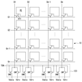
인셀 입력 센서 기술은 표시패널의 두께 증가 없이 표시패널에 입력 센서들을 설치할 수 있다. 인셀 입력 센서 기술은 표시패널의 픽셀들에 연결된 전극을 센서 전극으로 활용한다. 인셀 입력 센서 기술은 도 1과 같이 액정표시장치의 픽셀들(PXL)에 공통 전압을 공급하기 위한 공통 전극(COM)을 분할하여 입력 센서들의 센서 전극으로 활용할 수 있다. 센서 전극 각각은 다수의 픽셀들(PXL)과 중첩된다. 센서 전극들에는 공통 전압(Vcom)과 센서 구동 신호(Vdrv)를 선택적으로 인가하기 위해 센서 배선들(SL)이 연결된다. 인셀 입력 센서 기술은 한 프레임을 화상데이터 기입 기간과 센서 구동 기간으로 시분할하고, 화상데이터 기입 기간 동안 센서 전극들에 픽셀의 기준 전압인 공통 전압(Vcom)을 공급하고, 센서 구동 기간 동안 센서 전극들에 센서 구동 신호(Vdrv)를 공급한다.In-cell input sensor technology allows input sensors to be placed on the display panel without increasing the thickness of the display panel. The Insel input sensor technology utilizes the electrode connected to the pixels of the display panel as the sensor electrode. 1, a common electrode COM for supplying a common voltage to pixels PXL of a liquid crystal display can be divided into a sensor electrode of input sensors. Each of the sensor electrodes overlaps with a plurality of pixels PXL. Sensor wirings SL are connected to the sensor electrodes to selectively apply the common voltage Vcom and the sensor driving signal Vdrv. The in-cell input sensor technology divides one frame into an image data writing period and a sensor driving period, supplies a common voltage Vcom, which is a reference voltage of a pixel, to sensor electrodes during an image data writing period, And supplies the sensor driving signal Vdrv to the sensor driver.
이러한 종래 인셀 입력 센서 기술은 센싱을 위해 별도의 센서 배선들이 필요하고, 센서 전극과 센서 배선을 연결하기 위한 콘택홀 공정이 필요하여 공정이 복잡해지는 단점이 있다.In this conventional inserting input sensor technology, separate sensor wiring is required for sensing, and a contact hole process for connecting the sensor electrode and the sensor wiring is required, which complicates the process.
또한, 종래 인셀 입력 센서 기술은 터치 입력뿐만 아니라 지문 입력까지 센싱할 수 있도록 고밀도 전극 패턴의 센서 전극들이 필요하다. 따라서, 종래 인셀 입력 센서 기술은 도 2와 같이 고밀도 전극 패턴에 대응하여 n*m 개의 센싱 채널들이 필요한데, 제한된 면적 내에서 센싱 채널들을 늘리는 데에는 물리적으로 한계가 있다.In addition, the conventional inserting input sensor technology requires sensor electrodes having a high density electrode pattern so as to sense not only a touch input but also a fingerprint input. Therefore, in the conventional in-cell input sensor technology, as shown in FIG. 2, n * m sensing channels are required corresponding to a high-density electrode pattern. However, there is a physical limit to increase sensing channels within a limited area.
따라서, 본 발명의 목적은 간소한 공정으로 인셀 입력 센서 기술을 구현할 수 있도록 한 표시 장치와 그 구동방법을 제공하는 데 있다.Accordingly, it is an object of the present invention to provide a display device and a method of driving the same that can realize an inserting input sensor technology by a simple process.
상기 목적을 달성하기 위하여, 본 발명에 따른 표시장치는 표시패널과, 센싱 인에이블 신호를 생성하여 상기 1 스캔 타임 내에서 센서 구동 기간과 화상데이터 기입 기간을 정의하는 타이밍 콘틀롤러와, 센서 구동신호를 출력하는 센서 구동부와, 입력 영상의 디지털 비디오 데이터를 데이터 전압으로 변환하여 출력하는 데이터 구동부와, 스위치 어레이를 포함한다. 여기서, 표시패널에는 화소 전극을 갖는 다수의 픽셀들이 구비되고, 상기 화소 전극이 게이트라인으로부터 입력되는 스캔 신호의 1 스캔 타임 동안 데이터라인에 연결된다. 그리고, 스위치 어레이는 상기 센싱 인에이블 신호에 따라 스위칭되어, 상기 센서 구동 기간 동안 상기 센서 구동부의 출력을 상기 데이터라인에 공급하고, 상기 화상데이터 기입 기간 동안 상기 데이터 구동부의 출력을 상기 데이터라인에 공급한다.According to an aspect of the present invention, there is provided a display device including a display panel, a timing controller for generating a sensing enable signal to define a sensor driving period and an image data writing period within the one scan time, A data driver for converting the digital video data of the input video into a data voltage and outputting the data voltage, and a switch array. Here, the display panel includes a plurality of pixels having pixel electrodes, and the pixel electrodes are connected to the data lines for one scan time of the scan signals input from the gate lines. The switch array is switched according to the sensing enable signal to supply the output of the sensor driver to the data line during the sensor driving period and supplies the output of the data driving unit to the data line during the image data writing period do.
상기 센서 구동 기간 동안 상기 화소 전극에는 상기 센서 구동신호가 인가되고, 상기 센서 구동부는 상기 센서 구동 기간 동안 상기 데이터라인을 통해 읽어 들인 상기 화소 전극의 정전 용량 변화를 바탕으로 터치 입력 또는 지문 입력을 센싱한다.The sensor driving signal is applied to the pixel electrode during the sensor driving period and the sensor driving unit senses a touch input or a fingerprint input based on the capacitance change of the pixel electrode read through the data line during the sensor driving period do.
상기 표시패널은 미리 설정된 지문 센싱 영역과, 상기 지문 센싱 영역 이외의 터치 센싱 영역을 포함한다.The display panel includes a preset fingerprint sensing area and a touch sensing area other than the fingerprint sensing area.
상기 터치 센싱 영역을 대상으로 하여 터치 입력을 센싱하는 경우, 상기 센서 구동부는 복수의 데이터라인들로부터 입력되는 상기 화소 전극의 정전 용량 변화를 통합(Integration) 한다.When the touch input is sensed with respect to the touch sensing area, the sensor driver integrates the electrostatic capacitance changes of the pixel electrodes inputted from the plurality of data lines.
상기 지문 센싱 영역을 대상으로 하여 지문 입력을 센싱하는 경우, 상기 센서 구동부는 각 데이터라인으로부터 입력되는 상기 화소 전극의 정전 용량 변화를 개별 센싱한다.When sensing a fingerprint input with respect to the fingerprint sensing area, the sensor driver individually senses a capacitance change of the pixel electrode input from each data line.
상기 지문 센싱 영역에 속하는 픽셀들에는 특정 계조의 동일한 데이터 전압이 공급된다.Pixels belonging to the fingerprint sensing region are supplied with the same data voltage of a specific gradation.
상기 지문 센싱 영역에 속하는 픽셀들에는 데이터 전압의 공급이 차단된다.The supply of the data voltage to the pixels belonging to the fingerprint sensing area is interrupted.
상기 1 스캔 타임 내에서 상기 센서 구동 기간이 상기 화상데이터 기입 기간에 비해 앞선다.The sensor driving period is ahead of the image data writing period within the one scan time.
또한, 본 발명에 따른 표시장치의 구동방법은 화소 전극을 갖는 다수의 픽셀들이 구비되고, 상기 화소 전극이 게이트라인으로부터 입력되는 스캔 신호의 1 스캔 타임 동안 데이터라인에 연결되는 표시패널을 포함한 표시장치의 구동방법으로서, 상기 1 스캔 타임 내에서 센서 구동 기간과 화상데이터 기입 기간을 정의하기 위해 센싱 인에이블 신호를 생성하는 단계와, 센서 구동신호를 출력하는 단계와, 입력 영상의 디지털 비디오 데이터를 데이터 전압으로 변환하여 출력하는 단계와, 상기 센싱 인에이블 신호를 기초로 하여, 상기 센서 구동 기간 동안 상기 센서 구동신호를 상기 데이터라인에 공급하고, 상기 화상데이터 기입 기간 동안 상기 데이터 전압을 상기 데이터라인에 공급하는 단계를 포함한다.A method of driving a display device according to the present invention is a method of driving a display device including a plurality of pixels having pixel electrodes and a display panel including a display panel in which the pixel electrodes are connected to data lines for one scan time of a scan signal input from a gate line, The method comprising the steps of: generating a sensing enable signal to define a sensor driving period and an image data writing period within the one scan time; outputting a sensor driving signal; And supplying the sensor driving signal to the data line during the sensor driving period based on the sensing enable signal and outputting the data voltage to the data line during the image data writing period, .
본 발명은 인셀 입력 센서를 각 픽셀의 화소 전극으로 구현하고 데이터라인으로 기존의 센서 배선 역할을 대체케 함으로써, 입력 센서와 센서 배선 형성 공정, 및 그들을 연결하기 위한 콘택홀 공정을 스킵하여 입력 센서 공정을 획기적으로 간소화할 수 있다.The present invention realizes an insulator input sensor as a pixel electrode of each pixel and replaces the existing sensor wiring role with a data line, thereby skipping a contact hole forming process for connecting an input sensor and a sensor wiring, Can be dramatically simplified.
도 1은 종래 인셀 입력 센서 기술에서 센서 전극과 센서 배선을 보여주는 도면.
도 2는 종래 인셀 입력 센서 기술에서의 센싱 채널들을 보여주는 도면.
도 3은 본 발명의 실시예에 따라 픽셀의 화소 전극을 센서 전극으로 활용하는 표시장치를 보여주는 도면.
도 4는 1 스캔 타임 내에서 화상데이터 기입 기간과 센서 구동 기간을 정의하는 센싱 인에이블 신호를 보여주는 도면.
도 5는 데이터라인을 센서 배선으로 활용하기 위한 스위치 어레이를 보여주는 도면.
도 6은 센서 구동 기간 동안 센서 구동부와 스위치 어레이의 동작을 보여주는 도면.
도 7은 화상데이터 기입 기간 동안 데이터 구동부와 스위치 어레이의 동작을 보여주는 도면.
도 8은 데이터라인을 센서 구동부에 연결하기 위한 제1 스위치의 온 타임과, 데이터라인을 데이터 구동부에 연결하기 위한 제2 스위치의 온 타임이 스캔 신호에 동기되는 것을 보여주는 도면.
도 9는 특정 스캔 타임 내에서 터치 센싱 동작과 화상데이터 기입 동작을 자세히 보여주는 도면.
도 10은 특정 스캔 타임 내에서 지문 센싱 동작과 화상데이터 기입 동작을 자세히 보여주는 도면.
도 11은 지문 센싱 영역을 대상으로 화상데이터 기입 동작이 중지되는 일 예를 보여주는 도면.
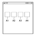
도 12 및 도 13은 지문 센싱 영역을 설정하는 일 예를 보여주는 도면들.1 is a view showing a sensor electrode and a sensor wiring in a conventional inserting input sensor technology.
2 is a view showing sensing channels in a conventional inserting input sensor technology.
3 is a view illustrating a display device utilizing a pixel electrode of a pixel as a sensor electrode according to an embodiment of the present invention.
4 is a diagram showing a sensing enable signal for defining an image data writing period and a sensor driving period within one scan time;
5 is a view showing a switch array for utilizing a data line as a sensor wiring.
6 is a view showing the operation of the sensor driver and the switch array during the sensor driving period.
7 is a view showing the operation of the data driver and the switch array during the image data writing period.
8 is a view showing that the on time of the first switch for connecting the data line to the sensor driver and the on time of the second switch for connecting the data line to the data driver are synchronized with the scan signal.
FIG. 9 is a view showing details of a touch sensing operation and an image data write operation within a specific scan time; FIG.
FIG. 10 is a view showing details of a fingerprint sensing operation and an image data writing operation within a specific scan time; FIG.
11 is a diagram showing an example in which an image data write operation is stopped with respect to a fingerprint sensing area;
12 and 13 are views showing an example of setting a fingerprint sensing area.
이하 첨부된 도면을 참조하여 본 발명에 따른 바람직한 실시예들을 상세히 설명한다. 명세서 전체에 걸쳐서 동일한 참조번호들은 실질적으로 동일한 구성요소들을 의미한다. 이하의 설명에서, 본 발명과 관련된 공지 기능 혹은 구성에 대한 구체적인 설명이 본 발명의 요지를 불필요하게 흐릴 수 있다고 판단되는 경우, 그 상세한 설명을 생략한다. DETAILED DESCRIPTION OF THE PREFERRED EMBODIMENTS Reference will now be made in detail to the preferred embodiments of the present invention, examples of which are illustrated in the accompanying drawings. Like reference numerals throughout the specification denote substantially identical components. In the following description, a detailed description of known functions and configurations incorporated herein will be omitted when it may make the subject matter of the present invention rather unclear.
본 발명에 따른 표시장치는 액정표시소자(Liquid Crystal Display, LCD), 전계방출 표시소자(Field Emission Display : FED), 플라즈마 디스플레이 패널(Plasma Display Panel, PDP), 유기발광 다이오드 표시소자(Organic Light Emitting Display, OLED), 전기영동 표시소자(Electrophoresis, EPD) 등의 평판 표시소자를 기반으로 구현될 수 있다. 이하의 실시예에서, 평판 표시소자는 액정표시소자를 중심으로 설명되지만, 본 발명의 표시장치는 액정표시소자에 한정되지 않는다. The display device according to the present invention may be applied to a liquid crystal display (LCD), a field emission display (FED), a plasma display panel (PDP), an organic light emitting diode A display, an OLED, and an electrophoresis (EPD) display device. In the following embodiments, the flat panel display element will be described mainly on the liquid crystal display element, but the display device of the present invention is not limited to the liquid crystal display element.
도 3은 본 발명의 실시예에 따라 픽셀의 화소 전극을 센서 전극으로 활용하는 표시장치를 보여준다. 도 4는 1 스캔 타임 내에서 화상데이터 기입 기간과 센서 구동 기간을 정의하는 센싱 인에이블 신호를 보여준다. 도 5는 데이터라인을 센서 배선으로 활용하기 위한 스위치 어레이를 보여준다. 도 6은 센서 구동 기간 동안 센서 구동부와 스위치 어레이의 동작을 보여준다. 도 7은 화상데이터 기입 기간 동안 데이터 구동부와 스위치 어레이의 동작을 보여준다. 그리고, 도 8은 데이터라인을 센서 구동부에 연결하기 위한 제1 스위치의 온 타임과, 데이터라인을 데이터 구동부에 연결하기 위한 제2 스위치의 온 타임이 스캔 신호에 동기되는 것을 보여준다.3 illustrates a display device that utilizes a pixel electrode of a pixel as a sensor electrode according to an embodiment of the present invention. FIG. 4 shows a sensing enable signal for defining the image data writing period and the sensor driving period within one scan time. 5 shows a switch array for utilizing a data line as a sensor wiring. 6 shows the operation of the sensor driver and the switch array during the sensor driving period. 7 shows the operation of the data driver and the switch array during the image data writing period. 8 shows that the ON time of the first switch for connecting the data line to the sensor driver and the ON time of the second switch for connecting the data line to the data driver are synchronized with the scan signal.
도 3 내지 도 8을 참조하면, 본 발명의 실시예에 따른 표시장치는 표시패널(10), 데이터 구동회로(12), 게이트 구동회로(14), 타이밍 콘트롤러(16), 및 호스트 시스템(19)을 포함한다.3 to 8, a display device according to an embodiment of the present invention includes a
표시패널(10)은 두 장의 기판들과, 그들 사이에 형성된 액정층을 포함한다. 액정층의 액정 분자들은 화소 전극(1,PE)에 인가되는 입력 영상의 데이터전압과, 공통전극(2)에 인가되는 공통 전압(Vcom)의 전위차로 발생되는 전계에 의해 구동된다. The
픽셀들 각각은 데이터 라인들(D1~Dm)과 게이트 라인들(G1~Gn)의 교차부들에 형성된 픽셀 TFT들(Thin Film Transistor), 픽셀 TFT를 통해 데이터 라인에 연결되는 화소 전극(1,PE), 공통 전압(Vcom)이 인가되는 공통전극(2), 화소 전극(1,PE)에 접속되어 액정셀의 전압을 유지시키기 위한 스토리지 커패시터(Storage Capacitor, Cst) 등을 포함한다. Each of the pixels includes pixel TFTs (Thin Film Transistors) formed at intersections of the data lines D1 to Dm and the gate lines G1 to Gn,
표시패널(10)의 상부 기판에는 블랙매트릭스, 컬러필터 등이 형성될 수 있다. 표시패널(10)의 하부 기판은 COT(Color filter On TFT) 구조로 구현될 수 있다. 이 경우에, 컬러필터는 표시패널(10)의 하부 기판에 형성될 수 있다. 표시패널(10)의 상부 기판과 하부 기판 각각에는 편광판이 부착되고 액정과 접하는 내면에 액정의 프리틸트각을 설정하기 위한 배향막이 형성된다. 표시패널(10)의 상부 기판과 하부 기판 사이에는 액정층의 셀갭(Cell gap)을 유지하기 위한 컬럼 스페이서가 형성된다. A black matrix, a color filter, or the like may be formed on the upper substrate of the
표시패널(10)의 배면 아래에는 백라이트 유닛이 배치될 수 있다. 백라이트 유닛은 에지형(edge type) 또는 직하형(Direct type) 백라이트 유닛으로 구현되어 표시패널(10)에 빛을 조사한다. 표시패널(10)은 TN(Twisted Nematic) 모드, VA(Vertical Alignment) 모드, IPS(In Plane Switching) 모드, FFS(Fringe Field Switching) 모드 등 공지된 어떠한 액정 모드로도 구현될 수 있다. 유기발광 다이오드 표시장치와 같은 자발광 표시장치에서 백라이트 유닛은 필요 없다.A backlight unit may be disposed under the rear surface of the
표시패널(10)의 픽셀 어레이는 인셀 입력 센서들을 내장한다. 인셀 입력 센서는 정전 용량 방식의 터치 센서와 지문 센서를 포함한다. 입력 센서 공정이 간소화되도록, 인셀 입력 센서는 각 픽셀의 화소 전극(1,PE)으로 구현된다. 데이터라인은 픽셀 TFT를 통해 화소 전극(1,PE)에 연결되며 기존의 센서 배선 역할을 대체한다. 본 발명에서는 별도의 센서 배선이 필요 없고, 따라서 센서 배선과 센서 전극을 전기적으로 연결하기 위한 콘택홀 공정도 필요 없다. 본 발명은 데이터 라인들을 통해 화소 전극들(1,PE)의 정전 용량 변화를 센싱하기 때문에 별도로 센싱 채널들이 추가되지 않는다.The pixel array of the
본 발명의 표시장치는 센서 구동 기간(Tt)과 화상데이터 기입 기간(Td)으로 시분할 구동된다. 픽셀 어레이의 화소 전극들(1,PE)에는 화상데이터 기입 기간(Td) 동안 입력 영상의 데이터전압(Vdata)이 기입된다. 센서 구동 기간(Tt) 동안, 화소 전극들(1,PE)에는 센서 구동 신호(Vdrv)가 인가되어 화소 전극들(1,PE)에 대한 터치 입력 또는 지문 입력이 센싱 된다.The display device of the present invention is time-division driven in the sensor driving period Tt and the image data writing period Td. The data voltage (Vdata) of the input image is written to the pixel electrodes (1, PE) of the pixel array during the image data writing period (Td). The sensor driving signal Vdrv is applied to the
인셀 입력 센서로 기능하는 화소 전극들(1,PE)에는 정전 용량이 연결된다. 정전 용량은 화소 전극(1,PE)에 걸리는 기생 용량을 포함한다. 화소 전극(1,PE)에 손가락과 같은 도전체가 접촉되면 정전 용량의 전하량이 변한다. 이러한 화소 전극(1,PE)의 정전 용량 변화량을 통해 터치 입력 또는 지문 입력이 감지된다.Electrostatic capacitance is connected to the pixel electrodes (1, PE) functioning as the in-cell input sensor. The capacitance includes the parasitic capacitance which is applied to the pixel electrodes (1, PE). When a conductor such as a finger touches the pixel electrode (1, PE), the amount of charge of the capacitance changes. A touch input or a fingerprint input is detected through the capacitance change amount of the pixel electrode (1, PE).
표시패널(10)은 미리 설정된 지문 센싱 영역과, 이 지문 센싱 영역 이외의 터치 센싱 영역을 포함한다. 지문 센싱 영역을 설정하는 예들에 대해서는 도 12 및 도 13을 참조하여 후술한다.The
타이밍 콘트롤러(16)는 호스트 시스템(19)으로부터 입력되는 수직 동기신호(Vsync), 수평 동기신호(Hsync), 데이터 인에이블 신호(Data Enable, DE), 메인 클럭(MCLK) 등의 타이밍신호를 입력받아 데이터 구동회로(12)와 게이트 구동회로(14)의 동작 타이밍을 동기시킨다. 스캔 타이밍 제어신호는 게이트 스타트 펄스(Gate Start Pulse, GSP), 게이트 쉬프트 클럭(Gate Shift Clock, GSC), 게이트 출력 인에이블신호(Gate Output Enable, GOE) 등을 포함한다. 데이터 타이밍 제어신호는 소스 샘플링 클럭(Source Sampling Clock, SSC), 극성제어신호(Polarity, POL), 소스 출력 인에이블신호(Source Output Enable, SOE) 등을 포함한다.The
타이밍 콘트롤러(16)는 도 4와 같은 센싱 인에이블 신호(TEN)를 생성하여 1 스캔 타임(1H) 내에서 센서 구동 기간(Tt)과 화상데이터 기입 기간(Td)을 정의한다. 센싱 인에이블 신호(TEN)는 센서 구동 기간(Tt) 동안에 제1 로직 레벨(L1)을 가지며, 화상데이터 기입 기간(Td) 동안에 제2 로직 레벨(L2)을 가진다. 1 스캔 타임(1H)은 표시패널(10)의 1 수평 픽셀 라인에 배치된 픽셀들에 대한 센싱 및 화상데이터 기입에 소요되는 시간으로 정의된다.The
호스트 시스템(19)은 디지털 비디오 데이터(RGB)와 함께 타이밍 신호들(Vsync, Hsync, DE, MCLK)을 타이밍 콘트롤러(16)로 전송하며, 데이터 구동회로(12)의 센서 구동부(121)로부터 입력되는 센싱 정보(XY)와 연계된 응용 프로그램을 실행할 수 있다.The
데이터 구동회로(12)는 센서 구동부(121)와, 데이터 구동부(122)와, 스위치 어레이(123)를 포함한다. 센서 구동부(121)와 데이터 구동부(122)와 스위치 어레이(123)는 센싱 인에이블 신호(TEN)에 동기하여 동작한다.The
센서 구동부(121)는 센서 구동 기간(Tt) 동안 센서 구동신호(Vdrv)를 출력하고, 센서 구동 기간(Tt) 동안 데이터라인을 통해 읽어 들인 화소전극(PE)의 정전 용량 변화를 바탕으로 터치 입력 또는 지문 입력을 센싱한다.The
데이터 구동부(122)는 화상데이터 기입 기간(Td) 동안 입력 영상의 디지털 비디오 데이터(RGB)를 데이터전압(Vdata)으로 변환하여 출력한다. The
스위치 어레이(123)는 도 5와 같이 센싱 인에이블 신호(TEN)에 따라 스위칭되는 다수의 제1 스위치들(SWT)과 다수의 제2 스위치들(SWD)을 포함하여, 센서 구동 기간(Tt) 동안 센서 구동부(121)의 출력을 데이터라인들(D1~Dm)에 공급하고, 화상데이터 기입 기간(Td) 동안 데이터 구동부(122)의 출력을 데이터라인들(D1~Dm)에 공급한다.The
제1 스위치들(SWT)은 센싱 인에이블 신호(TEN)의 제1 로직 레벨(L1)에 따라 턴 온 되어, 도 6과 같이 센서 구동부(121)로부터 입력되는 센서 구동신호(Vdrv)를 데이터라인들(D1~Dm)에 공급한다. 이 센서 구동신호(Vdrv)는 데이터라인들(D1~Dm)을 통해 화소전극들(PE)에 인가된다. 제1 스위치들(SWT)은 N 타입 트랜지스터로 구현될 수 있다. The first switches SWT are turned on according to the first logic level L1 of the sensing enable signal TEN to output the sensor driving signal Vdrv input from the
제2 스위치들(SWD)은 센싱 인에이블 신호(TEN)의 제2 로직 레벨(L2)에 따라 턴 온 되어, 도 7과 같이 데이터 구동부(122)로부터 입력되는 데이터 전압(Vdata)을 데이터라인들(D1~Dm)에 공급한다. 이 데이터 전압(Vdata)은 데이터라인들(D1~Dm)을 통해 화소전극들(PE)에 인가된다. 제2 스위치들(SWD)은 P 타입 트랜지스터로 구현될 수 있다.The second switches SWD are turned on according to the second logic level L2 of the sensing enable signal TEN to turn on the data voltage Vdata input from the
게이트 구동회로(14)는 도 8과 같이 1 스캔 타임(1H)에 대응되는 스캔 신호(SP)를 생성하여 게이트라인들(G1~Gn)에 라인 순차 방식으로 공급한다. 1 스캔 타임(1H) 내에서 센서 구동 기간(Tt)이 화상데이터 기입 기간(Td)에 비해 앞서며, 그에 따라 제1 스위치들(SWT)이 먼저 턴 온 되고 난 후, 제2 스위치들(SWD)이 턴 온 된다. 터치 센싱 또는 지문 센싱은 표시패널(10)에 기입된 화상데이터가 충분히 세츄레이션 되고 난 다음에 수행되는 것이 노이즈 회피 면에서 유리하다. 만약, 1 스캔 타임(1H) 내에서 화상데이터 기입 직후에 입력 센서를 구동시키면 과도 상태의 화상 데이터가 터치 또는 지문 센싱에 영향을 미쳐 센싱의 정확도를 떨어뜨릴 수 있다. 본 발명은 화상데이터 기입 시점으로부터 대략 1 프레임 이후에 입력 센서를 구동시키기 때문에 이러한 문제점을 미연에 방지할 수 있다.The
도 9는 특정 스캔 타임 내에서 터치 센싱 동작과 화상데이터 기입 동작을 자세히 보여준다.FIG. 9 shows details of the touch sensing operation and the image data write operation within a specific scan time.
도 9를 참조하면, x(x는 양의 정수) 번째 스캔 타임(1H) 동안 터치 센싱 영역을 대상으로 한 터치 센싱 동작과 화상데이터 기입 동작이 순차적으로 예시된다. Referring to FIG. 9, a touch sensing operation and an image data write operation for a touch sensing region during x (x is a positive integer) scan time (1H) are sequentially illustrated.
x 번째 스캔 타임(1H)의 센서 구동 기간(Tt) 동안, 센서 구동부(121)는 센서 구동신호(Vdrv)를 생성하여 제1 스위치들(SWT)과 데이터라인들(D1~Dm)을 통해 터치 센싱 영역에 속하는 화소전극들(PE)에 인가한다. 그리고, 이와 동시에 그 화소전극들(PE)로부터 입력되는 전하를 누적하여 센싱 전압(Vsen)을 생성한다. 하나의 화소전극(PE)로부터 입력되는 전하량은 매우 작으므로 터치 입력을 정확히 판단하기에 충분치 않다. 따라서, 센서 구동부(121)는 터치 센싱 영역을 대상으로 하여 터치 입력을 센싱하는 경우, 적어도 2개 이상의 데이터라인들로부터 입력되는 화소전극(PE)의 정전 용량 변화를 통합(Integration)할 수 있다. 이를 위해, 센서 구동부(121)는 다수의 데이터라인들로부터 입력되는 센싱값들을 통합할 수 있는 적분기로 구현될 수 있다. During the sensor driving period Tt of the
x 번째 스캔 타임(1H)의 화상데이터 기입 기간(Td) 동안, 데이터 구동부(122)는 데이터전압(Vdata_R,Vdata_G,Vdata_B)을 생성하여 제2 스위치들(SWD)과 데이터라인들(D1~Dm)을 통해 터치 센싱 영역에 속하는 화소전극들(PE)에 인가한다. the
도 10은 특정 스캔 타임 내에서 지문 센싱 동작과 화상데이터 기입 동작을 자세히 보여준다.10 shows details of the fingerprint sensing operation and the image data writing operation within a specific scan time.
도 10을 참조하면, x 번째 스캔 타임(1H) 동안 지문 센싱 영역을 대상으로 한 지문 센싱 동작과 화상데이터 기입 동작이 순차적으로 예시된다. Referring to FIG. 10, a fingerprint sensing operation and an image data writing operation are sequentially performed for the fingerprint sensing area during the x-th scan time (1H).
x 번째 스캔 타임(1H)의 센서 구동 기간(Tt) 동안, 센서 구동부(121)는 센서 구동신호(Vdrv)를 생성하여 제1 스위치들(SWT)과 데이터라인들(D1~Dm)을 통해 지문 센싱 영역에 속하는 화소전극들(PE)에 인가한다. 그리고, 이와 동시에 그 화소전극들(PE)로부터 입력되는 전하를 누적하여 센싱 전압(Vsen)을 생성한다. 이때, 지문 감지를 위해서는 세밀한 센싱이 필요하므로, 센서 구동부(121)는 지문 센싱 영역을 대상으로 하여 지문 입력을 센싱하는 경우, 각 데이터라인으로부터 입력되는 화소전극(PE)의 정전 용량 변화를 개별 센싱하여 센싱값들(Vsen1,Vsen2,Vsen3)을 획득한다. During the sensor driving period Tt of the
x 번째 스캔 타임(1H)의 화상데이터 기입 기간(Td) 동안, 데이터 구동부(122)는 특정 계조의 데이터전압(Vdata)을 생성하여 제2 스위치들(SWD)과 데이터라인들(D1~Dm)을 통해 지문 센싱 영역에 속하는 화소전극들(PE)에 공통으로 인가할 수 있다. 지문 센싱 영역은 지문 센싱시 손가락 등에 의해 덮혀지는 영역이므로, 지문 센싱 동안 어떠한 영상이 표시되어도 무방하기 때문이다.the
한편, 지문 센싱 영역에 속하는 픽셀들에는 데이터 전압의 공급이 차단될 수도 있다. 이를 위해, 도 11과 같이 화상 데이터 기입을 위한 제2 스위치들(SWD)은 1 스캔 타임(1H) 내내 턴 오프 상태를 유지할 수 있다. 타이밍 콘트롤러는 센싱 인에이블 신호(TEN) 이외에 추가적인 제어신호(미도시)를 더 생성하여 지문 센싱 영역에 속하는 픽셀들을 구동하는 제2 스위치들(SWD)의 동작을 턴 오프 시킬 수 있다.On the other hand, the supply of the data voltage may be interrupted to the pixels belonging to the fingerprint sensing area. For this purpose, as shown in FIG. 11, the second switches SWD for writing image data can maintain the turn-off state within one scan time (1H). The timing controller may generate an additional control signal (not shown) in addition to the sensing enable signal TEN to turn off the operation of the second switches SWD driving the pixels belonging to the fingerprint sensing area.
도 12 및 도 13은 지문 센싱 영역을 설정하는 일 예들을 보여준다.12 and 13 show examples of setting the fingerprint sensing area.
도 12를 참조하면, 지문 센싱 영역은 터치 지점의 위치 정보를 기반으로 자동으로 설정될 수 있다. 보안이 필요한 폴더 접근, 어플 실행, 및 콘텐츠 사용시, 사용자가 원하는 아이콘을 터치하면, 호스트 시스템은 터치 지점의 위치 정보를 취득하고, 취득된 위치를 포함한 특정 영역(D)을 지문 센싱 영역으로 설정할 수 있다. 도 12에서, D는 표시패널의 화면 상에 디스플레이되는 보안 폴더, 보안 어플, 보안 콘텐츠 중 어느 하나로서, 그 위치가 미리 지정되어 있다.Referring to FIG. 12, the fingerprint sensing area can be automatically set based on the position information of the touch point. When accessing a folder requiring security, executing an application, and using a content, the host system obtains position information of the touch point and sets a specific area (D) including the acquired position as a fingerprint sensing area have. In FIG. 12, D denotes any one of a security folder, a security application, and a secure content displayed on the screen of the display panel, and its location is previously specified.
한편, 도 13과 같이 터치 지점과 무관하게, 표시패널의 화면 상에 지문 센싱 영역들(A1~A4)이 미리 설정될 수도 있다.13, the fingerprint sensing areas A1 to A4 may be preset on the screen of the display panel regardless of the touch point.
상술한 바와 같이, 본 발명은 인셀 입력 센서를 각 픽셀의 화소 전극으로 구현하고 데이터라인으로 기존의 센서 배선 역할을 대체케 함으로써, 입력 센서와 센서 배선 형성 공정, 및 그들을 연결하기 위한 콘택홀 공정을 스킵하여 입력 센서 공정을 획기적으로 간소화할 수 있다. As described above, the present invention realizes an input sensor, a sensor wiring forming process, and a contact hole process for connecting them by implementing an inserting input sensor as a pixel electrode of each pixel and replacing the existing sensor wiring role with a data line. It is possible to dramatically simplify the input sensor process.
이상 설명한 내용을 통해 당업자라면 본 발명의 기술사상을 일탈하지 아니하는 범위에서 다양한 변경 및 수정이 가능함을 알 수 있을 것이다. 따라서, 본 발명의 기술적 범위는 명세서의 상세한 설명에 기재된 내용으로 한정되는 것이 아니라 특허 청구의 범위에 의해 정하여져야만 할 것이다.It will be apparent to those skilled in the art that various modifications and variations can be made in the present invention without departing from the spirit or scope of the invention. Therefore, the technical scope of the present invention should not be limited to the contents described in the detailed description of the specification, but should be defined by the claims.
10 : 표시패널
12 : 데이터 구동회로
14 : 게이트 구동회로
16 : 타이밍 콘트롤러
121 : 센서 구동부
122 : 데이터 구동부
123 : 스위치 어레이
SWT : 제1 스위치
SWD : 제2 스위치10: display panel 12: data driving circuit
14: Gate driving circuit 16: Timing controller
121: Sensor driver 122: Data driver
123: switch array SWT: first switch
SWD: second switch
Claims (16)
센싱 인에이블 신호를 생성하여 상기 1 스캔 타임 내에서 센서 구동 기간과 화상데이터 기입 기간을 정의하는 타이밍 콘트롤러;
센서 구동신호를 출력하는 센서 구동부;
입력 영상의 디지털 비디오 데이터를 데이터 전압으로 변환하여 출력하는 데이터 구동부; 및
상기 센싱 인에이블 신호에 따라 스위칭되어, 상기 센서 구동 기간 동안 상기 센서 구동부의 출력을 상기 데이터라인에 공급하고, 상기 화상데이터 기입 기간 동안 상기 데이터 구동부의 출력을 상기 데이터라인에 공급하는 스위치 어레이를 포함한 표시장치.A display panel having a plurality of pixels having pixel electrodes, the pixel electrodes being connected to a data line during one scan time of a scan signal input from a gate line;
A timing controller for generating a sensing enable signal and defining a sensor driving period and an image data writing period within the one scan time;
A sensor driver for outputting a sensor drive signal;
A data driver for converting digital video data of an input video into a data voltage and outputting the data voltage; And
And a switch array which is switched in accordance with the sensing enable signal and supplies the output of the sensor driver to the data line during the sensor driving period and supplies the output of the data driver during the image data writing period to the data line Display device.
상기 센서 구동 기간 동안 상기 화소 전극에는 상기 센서 구동신호가 인가되고,
상기 센서 구동부는 상기 센서 구동 기간 동안 상기 데이터라인을 통해 읽어 들인 상기 화소 전극의 정전 용량 변화를 바탕으로 터치 입력 또는 지문 입력을 센싱하는 표시장치.The method according to claim 1,
The sensor driving signal is applied to the pixel electrode during the sensor driving period,
Wherein the sensor driver senses a touch input or a fingerprint input based on a capacitance change of the pixel electrode read through the data line during the sensor driving period.
상기 표시패널은 미리 설정된 지문 센싱 영역과, 상기 지문 센싱 영역 이외의 터치 센싱 영역을 포함하는 표시장치.The method according to claim 1,
Wherein the display panel includes a preset fingerprint sensing area and a touch sensing area other than the fingerprint sensing area.
상기 터치 센싱 영역을 대상으로 하여 터치 입력을 센싱하는 경우, 상기 센서 구동부는 복수의 데이터라인들로부터 입력되는 상기 화소 전극의 정전 용량 변화를 통합(Integration)하는 표시장치.The method of claim 3,
Wherein the sensor driver integrates the capacitance change of the pixel electrode input from the plurality of data lines when the touch input is sensed with respect to the touch sensing area.
상기 지문 센싱 영역을 대상으로 하여 지문 입력을 센싱하는 경우, 상기 센서 구동부는 각 데이터라인으로부터 입력되는 상기 화소 전극의 정전 용량 변화를 개별 센싱하는 표시장치.The method of claim 3,
Wherein the sensor driver individually senses a capacitance change of the pixel electrode inputted from each data line when the fingerprint input is sensed in the fingerprint sensing area.
상기 지문 센싱 영역에 속하는 픽셀들에는 특정 계조의 동일한 데이터 전압이 공급되는 표시장치.The method of claim 3,
Wherein the same data voltage of a specific gray level is supplied to pixels belonging to the fingerprint sensing area.
상기 지문 센싱 영역에 속하는 픽셀들에는 데이터 전압의 공급이 차단되는 표시장치.The method of claim 3,
Wherein the supply of the data voltage to the pixels belonging to the fingerprint sensing area is interrupted.
상기 1 스캔 타임 내에서 상기 센서 구동 기간이 상기 화상데이터 기입 기간에 비해 앞서는 표시장치.The method according to claim 1,
Wherein the sensor driving period is ahead of the image data writing period within the one scan time.
상기 1 스캔 타임 내에서 센서 구동 기간과 화상데이터 기입 기간을 정의하기 위해 센싱 인에이블 신호를 생성하는 단계;
센서 구동신호를 출력하는 단계;
입력 영상의 디지털 비디오 데이터를 데이터 전압으로 변환하여 출력하는 단계; 및
상기 센싱 인에이블 신호를 기초로 하여, 상기 센서 구동 기간 동안 상기 센서 구동신호를 상기 데이터라인에 공급하고, 상기 화상데이터 기입 기간 동안 상기 데이터 전압을 상기 데이터라인에 공급하는 단계를 포함한 표시장치의 구동방법.There is provided a method of driving a display device including a display panel having a plurality of pixels having pixel electrodes and the pixel electrodes connected to data lines for one scan time of a scan signal input from a gate line,
Generating a sensing enable signal to define a sensor driving period and an image data writing period within the one scan time;
Outputting a sensor drive signal;
Converting digital video data of an input image into a data voltage and outputting the data voltage; And
And supplying the sensor driving signal to the data line during the sensor driving period based on the sensing enable signal and supplying the data voltage to the data line during the image data writing period Way.
상기 센서 구동 기간 동안 상기 화소 전극에 상기 센서 구동신호를 인가한 후, 상기 데이터라인을 통해 읽어 들인 상기 화소 전극의 정전 용량 변화를 바탕으로 터치 입력 또는 지문 입력을 센싱하는 단계를 더 포함하는 표시장치의 구동방법.10. The method of claim 9,
And sensing the touch input or the fingerprint input based on the capacitance change of the pixel electrode read through the data line after applying the sensor driving signal to the pixel electrode during the sensor driving period, .
상기 표시패널은 미리 설정된 지문 센싱 영역과, 상기 지문 센싱 영역 이외의 터치 센싱 영역을 포함하는 표시장치의 구동방법.10. The method of claim 9,
Wherein the display panel includes a preset fingerprint sensing area and a touch sensing area other than the fingerprint sensing area.
상기 터치 센싱 영역을 대상으로 하여 터치 입력을 센싱하는 경우, 복수의 데이터라인들로부터 입력되는 상기 화소 전극의 정전 용량 변화는 통합(Integration)되는 표시장치의 구동방법.12. The method of claim 11,
Wherein a capacitance change of the pixel electrode input from a plurality of data lines is integrated when sensing a touch input with respect to the touch sensing area.
상기 지문 센싱 영역을 대상으로 하여 지문 입력을 센싱하는 경우, 각 데이터라인으로부터 입력되는 상기 화소 전극의 정전 용량 변화는 개별 센싱되는 표시장치의 구동방법.12. The method of claim 11,
Wherein a change in capacitance of the pixel electrode input from each data line is individually sensed when sensing a fingerprint input with respect to the fingerprint sensing area.
상기 지문 센싱 영역에 속하는 픽셀들에는 특정 계조의 동일한 데이터 전압이 공급되는 표시장치의 구동방법.12. The method of claim 11,
Wherein the same data voltage of a specific gray level is supplied to the pixels belonging to the fingerprint sensing area.
상기 지문 센싱 영역에 속하는 픽셀들에는 데이터 전압의 공급이 차단되는 표시장치의 구동방법.12. The method of claim 11,
Wherein the supply of the data voltage to the pixels belonging to the fingerprint sensing region is interrupted.
상기 1 스캔 타임 내에서 상기 센서 구동 기간이 상기 화상데이터 기입 기간에 비해 앞서는 표시장치의 구동방법.10. The method of claim 9,
Wherein the sensor driving period is ahead of the image data writing period within the one scan time.
Priority Applications (1)
| Application Number | Priority Date | Filing Date | Title |
|---|---|---|---|
| KR1020150152679A KR102420490B1 (en) | 2015-10-30 | 2015-10-30 | Display Device And Driving Method Of The Same |
Applications Claiming Priority (1)
| Application Number | Priority Date | Filing Date | Title |
|---|---|---|---|
| KR1020150152679A KR102420490B1 (en) | 2015-10-30 | 2015-10-30 | Display Device And Driving Method Of The Same |
Publications (2)
| Publication Number | Publication Date |
|---|---|
| KR20170051794A true KR20170051794A (en) | 2017-05-12 |
| KR102420490B1 KR102420490B1 (en) | 2022-07-14 |
Family
ID=58740118
Family Applications (1)
| Application Number | Title | Priority Date | Filing Date |
|---|---|---|---|
| KR1020150152679A Active KR102420490B1 (en) | 2015-10-30 | 2015-10-30 | Display Device And Driving Method Of The Same |
Country Status (1)
| Country | Link |
|---|---|
| KR (1) | KR102420490B1 (en) |
Cited By (3)
| Publication number | Priority date | Publication date | Assignee | Title |
|---|---|---|---|---|
| CN107704145A (en) * | 2017-09-29 | 2018-02-16 | 武汉天马微电子有限公司 | Display panel, its control method and display device |
| KR20200057377A (en) * | 2018-11-16 | 2020-05-26 | 엘지디스플레이 주식회사 | Display device |
| KR20210081907A (en) * | 2019-12-24 | 2021-07-02 | 엘지디스플레이 주식회사 | Touch driver, touch display device, driving method of the touch display device |
Citations (9)
| Publication number | Priority date | Publication date | Assignee | Title |
|---|---|---|---|---|
| KR20120057403A (en) * | 2010-11-26 | 2012-06-05 | 엘지디스플레이 주식회사 | Liquid crystal display device with a built in touch screen and driving mehtod thereof |
| KR20120111678A (en) * | 2011-04-01 | 2012-10-10 | 엘지디스플레이 주식회사 | Touch sensor integrated type display device |
| KR20140032344A (en) * | 2012-06-29 | 2014-03-14 | 보에 테크놀로지 그룹 컴퍼니 리미티드 | Capacitive in-cell touch-screen panel, touch-positioning method, and display device |
| KR20140046888A (en) * | 2012-10-11 | 2014-04-21 | 크루셜텍 (주) | User terminal including a fingerprint recognition area in the touch screen |
| KR20140075543A (en) * | 2012-12-11 | 2014-06-19 | 엘지디스플레이 주식회사 | Display device with integrated touch screen and method for driving the same |
| KR20150015735A (en) * | 2013-08-01 | 2015-02-11 | 삼성디스플레이 주식회사 | Liquid crystal display device integrated touch sensor |
| KR20150028402A (en) * | 2013-09-05 | 2015-03-16 | 엘지디스플레이 주식회사 | In-cell touch liquid crystal display module |
| KR20150080164A (en) * | 2013-12-30 | 2015-07-09 | 엘지디스플레이 주식회사 | Touch panel dispaly device |
| KR20150124507A (en) * | 2014-04-28 | 2015-11-06 | 엘지디스플레이 주식회사 | Touch sensing device and driving method thereof |
-
2015
- 2015-10-30 KR KR1020150152679A patent/KR102420490B1/en active Active
Patent Citations (9)
| Publication number | Priority date | Publication date | Assignee | Title |
|---|---|---|---|---|
| KR20120057403A (en) * | 2010-11-26 | 2012-06-05 | 엘지디스플레이 주식회사 | Liquid crystal display device with a built in touch screen and driving mehtod thereof |
| KR20120111678A (en) * | 2011-04-01 | 2012-10-10 | 엘지디스플레이 주식회사 | Touch sensor integrated type display device |
| KR20140032344A (en) * | 2012-06-29 | 2014-03-14 | 보에 테크놀로지 그룹 컴퍼니 리미티드 | Capacitive in-cell touch-screen panel, touch-positioning method, and display device |
| KR20140046888A (en) * | 2012-10-11 | 2014-04-21 | 크루셜텍 (주) | User terminal including a fingerprint recognition area in the touch screen |
| KR20140075543A (en) * | 2012-12-11 | 2014-06-19 | 엘지디스플레이 주식회사 | Display device with integrated touch screen and method for driving the same |
| KR20150015735A (en) * | 2013-08-01 | 2015-02-11 | 삼성디스플레이 주식회사 | Liquid crystal display device integrated touch sensor |
| KR20150028402A (en) * | 2013-09-05 | 2015-03-16 | 엘지디스플레이 주식회사 | In-cell touch liquid crystal display module |
| KR20150080164A (en) * | 2013-12-30 | 2015-07-09 | 엘지디스플레이 주식회사 | Touch panel dispaly device |
| KR20150124507A (en) * | 2014-04-28 | 2015-11-06 | 엘지디스플레이 주식회사 | Touch sensing device and driving method thereof |
Cited By (4)
| Publication number | Priority date | Publication date | Assignee | Title |
|---|---|---|---|---|
| CN107704145A (en) * | 2017-09-29 | 2018-02-16 | 武汉天马微电子有限公司 | Display panel, its control method and display device |
| CN107704145B (en) * | 2017-09-29 | 2020-09-01 | 武汉天马微电子有限公司 | Display panel, control method thereof, and display device |
| KR20200057377A (en) * | 2018-11-16 | 2020-05-26 | 엘지디스플레이 주식회사 | Display device |
| KR20210081907A (en) * | 2019-12-24 | 2021-07-02 | 엘지디스플레이 주식회사 | Touch driver, touch display device, driving method of the touch display device |
Also Published As
| Publication number | Publication date |
|---|---|
| KR102420490B1 (en) | 2022-07-14 |
Similar Documents
| Publication | Publication Date | Title |
|---|---|---|
| KR101588983B1 (en) | Display device and driving device thereof | |
| US9262024B2 (en) | Liquid crystal display panel including touch sensor and liquid crystal display using the same | |
| KR102401354B1 (en) | Touch sensor integrated type display device | |
| US9459717B2 (en) | In-cell touch display device | |
| KR101424331B1 (en) | Touch sensing apparatus and driving method thereof | |
| JP6549921B2 (en) | Display unit with touch detection function | |
| KR101642257B1 (en) | Display device integrated with touch screen | |
| KR101633174B1 (en) | Touch sensing device and driving method thereof | |
| CN110858111B (en) | Integrated touch display device | |
| US10048797B2 (en) | Display device with data line precharging at boundary between touch driving period and display driving period | |
| KR101731174B1 (en) | Touch sensor integrated type display device | |
| KR20170081068A (en) | Touch sensor integrated type display device | |
| KR20130132061A (en) | Touch sensing apparatus | |
| KR102098681B1 (en) | In cell touch liquid crystal display device | |
| KR102559085B1 (en) | Display device having touch sensor and driving method of the same | |
| KR102390170B1 (en) | Display device and driving method thereof | |
| KR102420490B1 (en) | Display Device And Driving Method Of The Same | |
| KR20120034502A (en) | Flat panel display with a built-in touch sensor and driving method thereof | |
| KR20160093442A (en) | Touch panel and touch display device including the same | |
| KR102272952B1 (en) | Touch sensing device and driving method thereof | |
| KR20170081017A (en) | Finger sensor integrated type touch screen panel and driving method of the same | |
| KR102520692B1 (en) | Touch sensing system | |
| KR102541935B1 (en) | Device For Detecting User Input | |
| KR20130035009A (en) | Display having touch sensor | |
| KR102321830B1 (en) | Method For Driving Of Touch Display Device |
Legal Events
| Date | Code | Title | Description |
|---|---|---|---|
| PA0109 | Patent application |
Patent event code: PA01091R01D Comment text: Patent Application Patent event date: 20151030 |
|
| PG1501 | Laying open of application | ||
| A201 | Request for examination | ||
| PA0201 | Request for examination |
Patent event code: PA02012R01D Patent event date: 20200902 Comment text: Request for Examination of Application Patent event code: PA02011R01I Patent event date: 20151030 Comment text: Patent Application |
|
| E902 | Notification of reason for refusal | ||
| PE0902 | Notice of grounds for rejection |
Comment text: Notification of reason for refusal Patent event date: 20211217 Patent event code: PE09021S01D |
|
| E701 | Decision to grant or registration of patent right | ||
| PE0701 | Decision of registration |
Patent event code: PE07011S01D Comment text: Decision to Grant Registration Patent event date: 20220628 |
|
| GRNT | Written decision to grant | ||
| PR0701 | Registration of establishment |
Comment text: Registration of Establishment Patent event date: 20220708 Patent event code: PR07011E01D |
|
| PR1002 | Payment of registration fee |
Payment date: 20220711 End annual number: 3 Start annual number: 1 |
|
| PG1601 | Publication of registration | ||
| PR1001 | Payment of annual fee |
Payment date: 20250616 Start annual number: 4 End annual number: 4 |