KR20170052492A - 기판 탑재대 및 기판 처리 장치 - Google Patents
기판 탑재대 및 기판 처리 장치 Download PDFInfo
- Publication number
- KR20170052492A KR20170052492A KR1020160144410A KR20160144410A KR20170052492A KR 20170052492 A KR20170052492 A KR 20170052492A KR 1020160144410 A KR1020160144410 A KR 1020160144410A KR 20160144410 A KR20160144410 A KR 20160144410A KR 20170052492 A KR20170052492 A KR 20170052492A
- Authority
- KR
- South Korea
- Prior art keywords
- substrate
- elastic sheet
- processing
- mount
- temperature
- Prior art date
- Legal status (The legal status is an assumption and is not a legal conclusion. Google has not performed a legal analysis and makes no representation as to the accuracy of the status listed.)
- Granted
Links
Images



Classifications
-
- H01L21/3065—
-
- H—ELECTRICITY
- H10—SEMICONDUCTOR DEVICES; ELECTRIC SOLID-STATE DEVICES NOT OTHERWISE PROVIDED FOR
- H10P—GENERIC PROCESSES OR APPARATUS FOR THE MANUFACTURE OR TREATMENT OF DEVICES COVERED BY CLASS H10
- H10P50/00—Etching of wafers, substrates or parts of devices
- H10P50/20—Dry etching; Plasma etching; Reactive-ion etching
- H10P50/24—Dry etching; Plasma etching; Reactive-ion etching of semiconductor materials
- H10P50/242—Dry etching; Plasma etching; Reactive-ion etching of semiconductor materials of Group IV materials
-
- H—ELECTRICITY
- H10—SEMICONDUCTOR DEVICES; ELECTRIC SOLID-STATE DEVICES NOT OTHERWISE PROVIDED FOR
- H10P—GENERIC PROCESSES OR APPARATUS FOR THE MANUFACTURE OR TREATMENT OF DEVICES COVERED BY CLASS H10
- H10P72/00—Handling or holding of wafers, substrates or devices during manufacture or treatment thereof
- H10P72/04—Apparatus for manufacture or treatment
- H10P72/0431—Apparatus for thermal treatment
- H10P72/0432—Apparatus for thermal treatment mainly by conduction
-
- H—ELECTRICITY
- H01—ELECTRIC ELEMENTS
- H01J—ELECTRIC DISCHARGE TUBES OR DISCHARGE LAMPS
- H01J37/00—Discharge tubes with provision for introducing objects or material to be exposed to the discharge, e.g. for the purpose of examination or processing thereof
- H01J37/32—Gas-filled discharge tubes
- H01J37/32431—Constructional details of the reactor
- H01J37/32715—Workpiece holder
- H01J37/32724—Temperature
-
- H01L21/02315—
-
- H01L21/32136—
-
- H01L21/324—
-
- H01L21/67098—
-
- H01L21/67248—
-
- H01L21/6831—
-
- H01L21/6835—
-
- H—ELECTRICITY
- H10—SEMICONDUCTOR DEVICES; ELECTRIC SOLID-STATE DEVICES NOT OTHERWISE PROVIDED FOR
- H10P—GENERIC PROCESSES OR APPARATUS FOR THE MANUFACTURE OR TREATMENT OF DEVICES COVERED BY CLASS H10
- H10P14/00—Formation of materials, e.g. in the shape of layers or pillars
- H10P14/60—Formation of materials, e.g. in the shape of layers or pillars of insulating materials
- H10P14/65—Formation of materials, e.g. in the shape of layers or pillars of insulating materials characterised by treatments performed before or after the formation of the materials
- H10P14/6502—Formation of materials, e.g. in the shape of layers or pillars of insulating materials characterised by treatments performed before or after the formation of the materials of treatments performed before formation of the materials
- H10P14/6512—Formation of materials, e.g. in the shape of layers or pillars of insulating materials characterised by treatments performed before or after the formation of the materials of treatments performed before formation of the materials by exposure to a gas or vapour
- H10P14/6514—Formation of materials, e.g. in the shape of layers or pillars of insulating materials characterised by treatments performed before or after the formation of the materials of treatments performed before formation of the materials by exposure to a gas or vapour by exposure to a plasma
-
- H—ELECTRICITY
- H10—SEMICONDUCTOR DEVICES; ELECTRIC SOLID-STATE DEVICES NOT OTHERWISE PROVIDED FOR
- H10P—GENERIC PROCESSES OR APPARATUS FOR THE MANUFACTURE OR TREATMENT OF DEVICES COVERED BY CLASS H10
- H10P50/00—Etching of wafers, substrates or parts of devices
- H10P50/20—Dry etching; Plasma etching; Reactive-ion etching
- H10P50/26—Dry etching; Plasma etching; Reactive-ion etching of conductive or resistive materials
- H10P50/264—Dry etching; Plasma etching; Reactive-ion etching of conductive or resistive materials by chemical means
- H10P50/266—Dry etching; Plasma etching; Reactive-ion etching of conductive or resistive materials by chemical means by vapour etching only
- H10P50/267—Dry etching; Plasma etching; Reactive-ion etching of conductive or resistive materials by chemical means by vapour etching only using plasmas
-
- H—ELECTRICITY
- H10—SEMICONDUCTOR DEVICES; ELECTRIC SOLID-STATE DEVICES NOT OTHERWISE PROVIDED FOR
- H10P—GENERIC PROCESSES OR APPARATUS FOR THE MANUFACTURE OR TREATMENT OF DEVICES COVERED BY CLASS H10
- H10P72/00—Handling or holding of wafers, substrates or devices during manufacture or treatment thereof
- H10P72/04—Apparatus for manufacture or treatment
- H10P72/0431—Apparatus for thermal treatment
-
- H—ELECTRICITY
- H10—SEMICONDUCTOR DEVICES; ELECTRIC SOLID-STATE DEVICES NOT OTHERWISE PROVIDED FOR
- H10P—GENERIC PROCESSES OR APPARATUS FOR THE MANUFACTURE OR TREATMENT OF DEVICES COVERED BY CLASS H10
- H10P72/00—Handling or holding of wafers, substrates or devices during manufacture or treatment thereof
- H10P72/06—Apparatus for monitoring, sorting, marking, testing or measuring
- H10P72/0602—Temperature monitoring
-
- H—ELECTRICITY
- H10—SEMICONDUCTOR DEVICES; ELECTRIC SOLID-STATE DEVICES NOT OTHERWISE PROVIDED FOR
- H10P—GENERIC PROCESSES OR APPARATUS FOR THE MANUFACTURE OR TREATMENT OF DEVICES COVERED BY CLASS H10
- H10P72/00—Handling or holding of wafers, substrates or devices during manufacture or treatment thereof
- H10P72/70—Handling or holding of wafers, substrates or devices during manufacture or treatment thereof for supporting or gripping
- H10P72/72—Handling or holding of wafers, substrates or devices during manufacture or treatment thereof for supporting or gripping using electrostatic chucks
-
- H—ELECTRICITY
- H10—SEMICONDUCTOR DEVICES; ELECTRIC SOLID-STATE DEVICES NOT OTHERWISE PROVIDED FOR
- H10P—GENERIC PROCESSES OR APPARATUS FOR THE MANUFACTURE OR TREATMENT OF DEVICES COVERED BY CLASS H10
- H10P72/00—Handling or holding of wafers, substrates or devices during manufacture or treatment thereof
- H10P72/70—Handling or holding of wafers, substrates or devices during manufacture or treatment thereof for supporting or gripping
- H10P72/74—Handling or holding of wafers, substrates or devices during manufacture or treatment thereof for supporting or gripping using temporarily an auxiliary support
-
- H—ELECTRICITY
- H10—SEMICONDUCTOR DEVICES; ELECTRIC SOLID-STATE DEVICES NOT OTHERWISE PROVIDED FOR
- H10P—GENERIC PROCESSES OR APPARATUS FOR THE MANUFACTURE OR TREATMENT OF DEVICES COVERED BY CLASS H10
- H10P95/00—Generic processes or apparatus for manufacture or treatments not covered by the other groups of this subclass
- H10P95/90—Thermal treatments, e.g. annealing or sintering
-
- H—ELECTRICITY
- H01—ELECTRIC ELEMENTS
- H01J—ELECTRIC DISCHARGE TUBES OR DISCHARGE LAMPS
- H01J2237/00—Discharge tubes exposing object to beam, e.g. for analysis treatment, etching, imaging
- H01J2237/20—Positioning, supporting, modifying or maintaining the physical state of objects being observed or treated
- H01J2237/2001—Maintaining constant desired temperature
Landscapes
- Physics & Mathematics (AREA)
- Engineering & Computer Science (AREA)
- Plasma & Fusion (AREA)
- Chemical & Material Sciences (AREA)
- Analytical Chemistry (AREA)
- Container, Conveyance, Adherence, Positioning, Of Wafer (AREA)
- Drying Of Semiconductors (AREA)
Abstract
Description
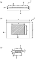
도 2는 탄성체 시트의 형상 및 눌림량을 설명하기 위한 도면,
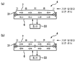
도 3은 본 발명의 제 1 실시형태에 있어서 제 1 부재 및 제 2 부재의 사이에 탄성체 시트를 개재하지 않을 때의 기판 탑재대 표면의 온도 분포예를 도시하는 모식도,
도 4는 본 발명의 제 1 실시형태에 있어서 제 1 부재 및 제 2 부재의 사이에 탄성체 시트를 개재시켰을 때의 기판 탑재대 표면의 온도 분포예를 도시하는 모식도,
도 5는 탄성체 시트를 마련하지 않는 경우와 마련한 경우에 대해, 기판 탑재대의 표면 온도의 시간 변화에 대해 실제로 측정한 결과를 나타내는 도면,
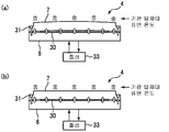
도 6은 본 발명의 제 2 실시형태에 따른 기판 탑재대를 도시하는 단면도,
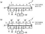
도 7은 본 발명의 제 2 실시예에 있어서 제 1 부재 및 제 2 부재의 사이에 탄성체 시트를 개재시키지 않을 때 및 개재시켰을 때의 기판 탑재대 표면의 온도 분포예를 도시하는 모식도.
4: 기판 탑재대 5: 절연 부재
6: 제 1 부재 7: 제 2 부재
8: 정전 척 9: 측벽 절연 부재
11: 샤워 헤드 15: 처리 가스 공급관
18: 처리 가스 공급원 19: 배기관
20: 배기 장치 21: 반입·반출구
25: 고주파 전원 30, 30': 탄성체 시트
31: 외측 나사 32: 냉매 유로
33: 칠러 37: 직류 전원
40: 제어부 41: 내측 나사
G: 기판
Claims (13)
- 처리 용기 내에서 피처리 기판에 처리를 실시하는 기판 처리 장치에서 기판을 탑재하는 기판 탑재대에 있어서,
베이스가 되는 금속제의 제 1 부재와,
상기 제 1 부재 상에 마련된 금속제의 제 2 부재와,
상기 제 2 부재의 표면에 마련된, 기판을 탑재하는 기판 탑재부와,
상기 제 1 부재에 마련된 온도 조절 수단과,
상기 제 1 부재 및 상기 제 2 부재의 사이에 개재되며, 유기 재료로 이루어지는 탄성체로 구성된 탄성체 시트와,
상기 탄성체 시트가 개재된 상태에서 상기 제 1 부재 및 상기 제 2 부재의 적어도 외주를 체결하는 체결 부재를 갖고,
상기 탄성체 시트는, 상기 체결 부재에 의해 상기 제 1 부재 및 상기 제 2 부재가 체결되었을 때에, 상기 제 1 부재 및 상기 제 2 부재의 사이에 형성되는 미소 간극을 메우는 것을 특징으로 하는
기판 탑재대. - 제 1 항에 있어서,
상기 제 1 부재 및 상기 제 2 부재는 이종(異種)의 금속으로 구성되어 있는 것을 특징으로 하는
기판 탑재대. - 제 1 항에 있어서,
상기 제 1 부재에 접속된, 고주파 전력을 공급하기 위한 고주파 전원을 추가로 갖는 것을 특징으로 하는
기판 탑재대. - 제 1 항에 있어서,
상기 온도 조절 수단은, 상기 제 1 부재의 내부에 마련된 온도 조절 매체 유로와, 온도 조절 매체 유로에 온도 조절 매체를 공급하는 온도 조절 매체 공급부를 갖는 것을 특징으로 하는
기판 탑재대. - 제 1 항에 있어서,
상기 기판 탑재부는 기판을 정전 흡착하기 위한 정전 척을 갖는 것을 특징으로 하는
기판 탑재대. - 제 1 항에 있어서,
상기 탄성체 시트는 영률이 1~40㎫인 것을 특징으로 하는
기판 탑재대. - 제 6 항에 있어서,
상기 탄성체 시트를 구성하는 재료가 실리콘 고무 또는 불소 고무인 것을 특징으로 하는
기판 탑재대. - 제 1 항에 있어서,
상기 기판은 직사각형 형상을 이루며, 상기 제 1 부재, 상기 제 2 부재 및 상기 탄성체 시트는 기판에 대응한 직사각형 형상을 이루는 것을 특징으로 하는
기판 탑재대. - 제 8 항에 있어서,
상기 제 1 부재 및 상기 제 2 부재의 장변에 대한 상기 탄성체 시트의 장변의 비율, 및 상기 제 1 부재 및 상기 제 2 부재의 단변에 대한 상기 탄성체 시트의 단변의 비율은 모두 0보다 크고 1보다 작은 것을 특징으로 하는
기판 탑재대. - 제 9 항에 있어서,
상기 제 1 부재 및 상기 제 2 부재의 장변에 대한 상기 탄성체 시트의 장변의 비율, 및 상기 제 1 부재 및 상기 제 2 부재의 단변에 대한 상기 탄성체 시트의 단변의 비율은 모두 0.3 이상, 0.9 이하인 것을 특징으로 하는
기판 탑재대. - 제 1 항에 있어서,
상기 탄성체 시트는, 초기의 두께를 t0으로 하고 상기 제 1 부재 및 상기 제 2 부재에 개재되어 눌린 두께를 t1로 한 경우에, t1/t0×100(%)으로 나타내는 눌림량이 50~70%인 것을 특징으로 하는
기판 탑재대. - 제 1 항에 있어서,
상기 제 1 부재 및 상기 제 2 부재는 이들의 외주부 및 내측 부분이 체결 부재에 의해 체결되고, 이들 체결 부재에 의해 체결되었을 때에 형성된 복수의 미소 간극에 각각 상기 탄성체 시트를 개재시키는 것을 특징으로 하는
기판 탑재대. - 피처리 기판에 대해 처리를 실시하기 위한 처리 용기와,
상기 처리 용기 내에서 기판을 탑재하는 제 1 항 내지 제 12 항 중 어느 한 항에 기재된 기판 탑재대와,
상기 처리 용기 내에 처리 가스를 공급하는 처리 가스 공급 기구와,
상기 처리 가스 공급 기구로부터 공급된 상기 처리 가스를 상기 처리 용기 내에 도입하는 처리 가스 도입부와,
상기 처리 용기 내를 배기하는 배기 기구를 구비하는 것을 특징으로 하는
기판 처리 장치.
Applications Claiming Priority (2)
| Application Number | Priority Date | Filing Date | Title |
|---|---|---|---|
| JP2015216551A JP6584289B2 (ja) | 2015-11-04 | 2015-11-04 | 基板載置台および基板処理装置 |
| JPJP-P-2015-216551 | 2015-11-04 |
Publications (2)
| Publication Number | Publication Date |
|---|---|
| KR20170052492A true KR20170052492A (ko) | 2017-05-12 |
| KR101928626B1 KR101928626B1 (ko) | 2018-12-12 |
Family
ID=58740285
Family Applications (1)
| Application Number | Title | Priority Date | Filing Date |
|---|---|---|---|
| KR1020160144410A Active KR101928626B1 (ko) | 2015-11-04 | 2016-11-01 | 기판 탑재대 및 기판 처리 장치 |
Country Status (4)
| Country | Link |
|---|---|
| JP (1) | JP6584289B2 (ko) |
| KR (1) | KR101928626B1 (ko) |
| CN (1) | CN107026102B (ko) |
| TW (1) | TWI705495B (ko) |
Cited By (1)
| Publication number | Priority date | Publication date | Assignee | Title |
|---|---|---|---|---|
| KR20200063055A (ko) * | 2018-11-27 | 2020-06-04 | 도쿄엘렉트론가부시키가이샤 | 플라스마 처리 장치 및 플라스마 처리 방법 |
Families Citing this family (6)
| Publication number | Priority date | Publication date | Assignee | Title |
|---|---|---|---|---|
| JP7090465B2 (ja) * | 2018-05-10 | 2022-06-24 | 東京エレクトロン株式会社 | 載置台及びプラズマ処理装置 |
| JP7133992B2 (ja) * | 2018-06-07 | 2022-09-09 | 東京エレクトロン株式会社 | 基板載置台及び基板処理装置 |
| US12542258B2 (en) | 2020-03-05 | 2026-02-03 | Mitsubishi Materials Corporation | Member for plasma processing apparatus, method for manufacturing same, and plasma processing apparatus |
| JP7301021B2 (ja) * | 2020-05-01 | 2023-06-30 | 東京エレクトロン株式会社 | 基板処理装置、載置台及び温度制御方法 |
| KR102700261B1 (ko) * | 2022-06-28 | 2024-08-28 | 엔지케이 인슐레이터 엘티디 | 웨이퍼 배치대 |
| WO2024232265A1 (ja) * | 2023-05-08 | 2024-11-14 | 東京エレクトロン株式会社 | 部材および部材の製造方法 |
Citations (4)
| Publication number | Priority date | Publication date | Assignee | Title |
|---|---|---|---|---|
| JP2001237222A (ja) * | 2000-02-22 | 2001-08-31 | Shibaura Mechatronics Corp | 真空処理装置 |
| KR20030081070A (ko) * | 2002-04-09 | 2003-10-17 | 마츠시타 덴끼 산교 가부시키가이샤 | 플라즈마 처리 방법 및 장치와 플라즈마 처리용 트레이 |
| KR20030082472A (ko) * | 2002-04-16 | 2003-10-22 | 아네르바 가부시키가이샤 | 정전 흡착 스테이지 및 기판 처리 장치 |
| JP2017001899A (ja) * | 2015-06-05 | 2017-01-05 | 旭硝子株式会社 | フロートガラス製造方法、及びフロートガラス製造装置 |
Family Cites Families (7)
| Publication number | Priority date | Publication date | Assignee | Title |
|---|---|---|---|---|
| US7431788B2 (en) * | 2005-07-19 | 2008-10-07 | Lam Research Corporation | Method of protecting a bond layer in a substrate support adapted for use in a plasma processing system |
| JP2007311613A (ja) * | 2006-05-19 | 2007-11-29 | Hitachi High-Technologies Corp | 試料台及びそれを備えたプラズマ処理装置 |
| CN101770971B (zh) * | 2008-12-31 | 2012-06-20 | 中芯国际集成电路制造(上海)有限公司 | 晶圆承载装置 |
| KR101219054B1 (ko) * | 2009-05-27 | 2013-01-18 | 도쿄엘렉트론가부시키가이샤 | 정전 흡착 전극 및 그 제조 방법, 그리고 기판 처리 장치 |
| US20120037068A1 (en) * | 2010-08-11 | 2012-02-16 | Applied Materials, Inc. | Composite substrates for direct heating and increased temperature uniformity |
| JP6010433B2 (ja) * | 2012-11-15 | 2016-10-19 | 東京エレクトロン株式会社 | 基板載置台および基板処理装置 |
| JP6296770B2 (ja) * | 2013-11-29 | 2018-03-20 | 日本特殊陶業株式会社 | 基板載置装置 |
-
2015
- 2015-11-04 JP JP2015216551A patent/JP6584289B2/ja active Active
-
2016
- 2016-10-24 TW TW105134301A patent/TWI705495B/zh active
- 2016-11-01 KR KR1020160144410A patent/KR101928626B1/ko active Active
- 2016-11-04 CN CN201610963595.XA patent/CN107026102B/zh active Active
Patent Citations (4)
| Publication number | Priority date | Publication date | Assignee | Title |
|---|---|---|---|---|
| JP2001237222A (ja) * | 2000-02-22 | 2001-08-31 | Shibaura Mechatronics Corp | 真空処理装置 |
| KR20030081070A (ko) * | 2002-04-09 | 2003-10-17 | 마츠시타 덴끼 산교 가부시키가이샤 | 플라즈마 처리 방법 및 장치와 플라즈마 처리용 트레이 |
| KR20030082472A (ko) * | 2002-04-16 | 2003-10-22 | 아네르바 가부시키가이샤 | 정전 흡착 스테이지 및 기판 처리 장치 |
| JP2017001899A (ja) * | 2015-06-05 | 2017-01-05 | 旭硝子株式会社 | フロートガラス製造方法、及びフロートガラス製造装置 |
Cited By (1)
| Publication number | Priority date | Publication date | Assignee | Title |
|---|---|---|---|---|
| KR20200063055A (ko) * | 2018-11-27 | 2020-06-04 | 도쿄엘렉트론가부시키가이샤 | 플라스마 처리 장치 및 플라스마 처리 방법 |
Also Published As
| Publication number | Publication date |
|---|---|
| JP6584289B2 (ja) | 2019-10-02 |
| CN107026102B (zh) | 2020-03-31 |
| JP2017092104A (ja) | 2017-05-25 |
| TW201730960A (zh) | 2017-09-01 |
| KR101928626B1 (ko) | 2018-12-12 |
| CN107026102A (zh) | 2017-08-08 |
| TWI705495B (zh) | 2020-09-21 |
Similar Documents
| Publication | Publication Date | Title |
|---|---|---|
| KR101928626B1 (ko) | 기판 탑재대 및 기판 처리 장치 | |
| US8282769B2 (en) | Shower head and plasma processing apparatus having same | |
| CN103107119B (zh) | 基板冷却系统、基板处理装置、静电吸盘及基板冷却方法 | |
| JP6345030B2 (ja) | プラズマ処理装置及びフォーカスリング | |
| CN108183058B (zh) | 载置台和等离子体处理装置 | |
| KR100929449B1 (ko) | 기판 처리 장치 및 포커스 링 | |
| US20030168439A1 (en) | Wafer stage for wafer processing apparatus and wafer processing method | |
| US20050000442A1 (en) | Upper electrode and plasma processing apparatus | |
| CN100431097C (zh) | 上部电极、等离子体处理装置和等离子体处理方法 | |
| TW200919622A (en) | Carrying bench and plasma treatment apparatus using the same | |
| JP7370228B2 (ja) | プラズマ処理装置 | |
| CN107086200A (zh) | 基板载置台和基板处理装置 | |
| JP5004436B2 (ja) | 静電吸着電極および処理装置 | |
| CN114373666B (zh) | 紧固构造、等离子体处理装置以及紧固方法 | |
| US8052364B2 (en) | Coupling member and plasma processing apparatus | |
| KR20160086272A (ko) | 냉각 구조물 및 평행 평판 에칭 장치 | |
| JP2001217304A (ja) | 基板ステージ、それを用いた基板処理装置および基板処理方法 | |
| JP2024105999A (ja) | 基板処理装置及び基板支持部 |
Legal Events
| Date | Code | Title | Description |
|---|---|---|---|
| A201 | Request for examination | ||
| PA0109 | Patent application |
St.27 status event code: A-0-1-A10-A12-nap-PA0109 |
|
| PA0201 | Request for examination |
St.27 status event code: A-1-2-D10-D11-exm-PA0201 |
|
| PG1501 | Laying open of application |
St.27 status event code: A-1-1-Q10-Q12-nap-PG1501 |
|
| D13-X000 | Search requested |
St.27 status event code: A-1-2-D10-D13-srh-X000 |
|
| D14-X000 | Search report completed |
St.27 status event code: A-1-2-D10-D14-srh-X000 |
|
| E902 | Notification of reason for refusal | ||
| PE0902 | Notice of grounds for rejection |
St.27 status event code: A-1-2-D10-D21-exm-PE0902 |
|
| AMND | Amendment | ||
| P11-X000 | Amendment of application requested |
St.27 status event code: A-2-2-P10-P11-nap-X000 |
|
| P13-X000 | Application amended |
St.27 status event code: A-2-2-P10-P13-nap-X000 |
|
| E601 | Decision to refuse application | ||
| PE0601 | Decision on rejection of patent |
St.27 status event code: N-2-6-B10-B15-exm-PE0601 |
|
| AMND | Amendment | ||
| E13-X000 | Pre-grant limitation requested |
St.27 status event code: A-2-3-E10-E13-lim-X000 |
|
| P11-X000 | Amendment of application requested |
St.27 status event code: A-2-2-P10-P11-nap-X000 |
|
| P13-X000 | Application amended |
St.27 status event code: A-2-2-P10-P13-nap-X000 |
|
| PX0901 | Re-examination |
St.27 status event code: A-2-3-E10-E12-rex-PX0901 |
|
| PX0701 | Decision of registration after re-examination |
St.27 status event code: A-3-4-F10-F13-rex-PX0701 |
|
| X701 | Decision to grant (after re-examination) | ||
| GRNT | Written decision to grant | ||
| PR0701 | Registration of establishment |
St.27 status event code: A-2-4-F10-F11-exm-PR0701 |
|
| PR1002 | Payment of registration fee |
St.27 status event code: A-2-2-U10-U11-oth-PR1002 Fee payment year number: 1 |
|
| PG1601 | Publication of registration |
St.27 status event code: A-4-4-Q10-Q13-nap-PG1601 |
|
| PR1001 | Payment of annual fee |
St.27 status event code: A-4-4-U10-U11-oth-PR1001 Fee payment year number: 4 |
|
| PR1001 | Payment of annual fee |
St.27 status event code: A-4-4-U10-U11-oth-PR1001 Fee payment year number: 5 |
|
| PR1001 | Payment of annual fee |
St.27 status event code: A-4-4-U10-U11-oth-PR1001 Fee payment year number: 6 |
|
| PR1001 | Payment of annual fee |
St.27 status event code: A-4-4-U10-U11-oth-PR1001 Fee payment year number: 7 |
|
| P22-X000 | Classification modified |
St.27 status event code: A-4-4-P10-P22-nap-X000 |