KR20170052760A - 표시장치 및 이의 제조 방법 - Google Patents
표시장치 및 이의 제조 방법 Download PDFInfo
- Publication number
- KR20170052760A KR20170052760A KR1020150154074A KR20150154074A KR20170052760A KR 20170052760 A KR20170052760 A KR 20170052760A KR 1020150154074 A KR1020150154074 A KR 1020150154074A KR 20150154074 A KR20150154074 A KR 20150154074A KR 20170052760 A KR20170052760 A KR 20170052760A
- Authority
- KR
- South Korea
- Prior art keywords
- guide plate
- light guide
- adhesive tape
- chassis
- fastening
- Prior art date
- Legal status (The legal status is an assumption and is not a legal conclusion. Google has not performed a legal analysis and makes no representation as to the accuracy of the status listed.)
- Granted
Links
- 239000002390 adhesive tape Substances 0.000 claims description 46
- 238000000034 method Methods 0.000 claims description 18
- 230000003287 optical effect Effects 0.000 claims description 12
- 230000008878 coupling Effects 0.000 claims description 11
- 238000010168 coupling process Methods 0.000 claims description 11
- 238000005859 coupling reaction Methods 0.000 claims description 11
- 238000004519 manufacturing process Methods 0.000 claims description 10
- 238000005452 bending Methods 0.000 claims description 9
- 239000000758 substrate Substances 0.000 description 20
- 101100372601 Saccharomyces cerevisiae (strain ATCC 204508 / S288c) POR2 gene Proteins 0.000 description 9
- 101100099673 Zea mays TIP2-3 gene Proteins 0.000 description 9
- 102100038779 Arfaptin-2 Human genes 0.000 description 8
- 101000809446 Homo sapiens Arfaptin-2 Proteins 0.000 description 8
- 239000010408 film Substances 0.000 description 7
- 239000010949 copper Substances 0.000 description 6
- 239000004973 liquid crystal related substance Substances 0.000 description 6
- 101100224481 Dictyostelium discoideum pole gene Proteins 0.000 description 5
- 101150110488 POL2 gene Proteins 0.000 description 5
- 230000010287 polarization Effects 0.000 description 4
- 239000010409 thin film Substances 0.000 description 4
- RYGMFSIKBFXOCR-UHFFFAOYSA-N Copper Chemical compound [Cu] RYGMFSIKBFXOCR-UHFFFAOYSA-N 0.000 description 3
- XEEYBQQBJWHFJM-UHFFFAOYSA-N Iron Chemical compound [Fe] XEEYBQQBJWHFJM-UHFFFAOYSA-N 0.000 description 3
- 101150046160 POL1 gene Proteins 0.000 description 3
- 101100117436 Thermus aquaticus polA gene Proteins 0.000 description 3
- 239000000853 adhesive Substances 0.000 description 3
- 230000001070 adhesive effect Effects 0.000 description 3
- 229910052782 aluminium Inorganic materials 0.000 description 3
- XAGFODPZIPBFFR-UHFFFAOYSA-N aluminium Chemical compound [Al] XAGFODPZIPBFFR-UHFFFAOYSA-N 0.000 description 3
- 150000001875 compounds Chemical class 0.000 description 3
- 229910052802 copper Inorganic materials 0.000 description 3
- 239000007769 metal material Substances 0.000 description 3
- 239000000203 mixture Substances 0.000 description 3
- 238000012986 modification Methods 0.000 description 3
- 230000004048 modification Effects 0.000 description 3
- 238000009792 diffusion process Methods 0.000 description 2
- 230000009977 dual effect Effects 0.000 description 2
- 230000000694 effects Effects 0.000 description 2
- 230000005684 electric field Effects 0.000 description 2
- 239000000463 material Substances 0.000 description 2
- 239000004020 conductor Substances 0.000 description 1
- 239000011521 glass Substances 0.000 description 1
- 238000001746 injection moulding Methods 0.000 description 1
- 239000011159 matrix material Substances 0.000 description 1
- 229920000642 polymer Polymers 0.000 description 1
- 238000002834 transmittance Methods 0.000 description 1
Images





Classifications
-
- G—PHYSICS
- G02—OPTICS
- G02B—OPTICAL ELEMENTS, SYSTEMS OR APPARATUS
- G02B6/00—Light guides; Structural details of arrangements comprising light guides and other optical elements, e.g. couplings
- G02B6/0001—Light guides; Structural details of arrangements comprising light guides and other optical elements, e.g. couplings specially adapted for lighting devices or systems
- G02B6/0011—Light guides; Structural details of arrangements comprising light guides and other optical elements, e.g. couplings specially adapted for lighting devices or systems the light guides being planar or of plate-like form
- G02B6/0081—Mechanical or electrical aspects of the light guide and light source in the lighting device peculiar to the adaptation to planar light guides, e.g. concerning packaging
- G02B6/0086—Positioning aspects
- G02B6/0088—Positioning aspects of the light guide or other optical sheets in the package
-
- G—PHYSICS
- G02—OPTICS
- G02F—OPTICAL DEVICES OR ARRANGEMENTS FOR THE CONTROL OF LIGHT BY MODIFICATION OF THE OPTICAL PROPERTIES OF THE MEDIA OF THE ELEMENTS INVOLVED THEREIN; NON-LINEAR OPTICS; FREQUENCY-CHANGING OF LIGHT; OPTICAL LOGIC ELEMENTS; OPTICAL ANALOGUE/DIGITAL CONVERTERS
- G02F1/00—Devices or arrangements for the control of the intensity, colour, phase, polarisation or direction of light arriving from an independent light source, e.g. switching, gating or modulating; Non-linear optics
- G02F1/01—Devices or arrangements for the control of the intensity, colour, phase, polarisation or direction of light arriving from an independent light source, e.g. switching, gating or modulating; Non-linear optics for the control of the intensity, phase, polarisation or colour
- G02F1/13—Devices or arrangements for the control of the intensity, colour, phase, polarisation or direction of light arriving from an independent light source, e.g. switching, gating or modulating; Non-linear optics for the control of the intensity, phase, polarisation or colour based on liquid crystals, e.g. single liquid crystal display cells
- G02F1/133—Constructional arrangements; Operation of liquid crystal cells; Circuit arrangements
- G02F1/1333—Constructional arrangements; Manufacturing methods
- G02F1/133308—Support structures for LCD panels, e.g. frames or bezels
-
- G—PHYSICS
- G02—OPTICS
- G02B—OPTICAL ELEMENTS, SYSTEMS OR APPARATUS
- G02B6/00—Light guides; Structural details of arrangements comprising light guides and other optical elements, e.g. couplings
- G02B6/0001—Light guides; Structural details of arrangements comprising light guides and other optical elements, e.g. couplings specially adapted for lighting devices or systems
- G02B6/0011—Light guides; Structural details of arrangements comprising light guides and other optical elements, e.g. couplings specially adapted for lighting devices or systems the light guides being planar or of plate-like form
- G02B6/0033—Means for improving the coupling-out of light from the light guide
- G02B6/005—Means for improving the coupling-out of light from the light guide provided by one optical element, or plurality thereof, placed on the light output side of the light guide
-
- G—PHYSICS
- G02—OPTICS
- G02B—OPTICAL ELEMENTS, SYSTEMS OR APPARATUS
- G02B6/00—Light guides; Structural details of arrangements comprising light guides and other optical elements, e.g. couplings
- G02B6/0001—Light guides; Structural details of arrangements comprising light guides and other optical elements, e.g. couplings specially adapted for lighting devices or systems
- G02B6/0011—Light guides; Structural details of arrangements comprising light guides and other optical elements, e.g. couplings specially adapted for lighting devices or systems the light guides being planar or of plate-like form
- G02B6/0081—Mechanical or electrical aspects of the light guide and light source in the lighting device peculiar to the adaptation to planar light guides, e.g. concerning packaging
- G02B6/0083—Details of electrical connections of light sources to drivers, circuit boards, or the like
-
- G—PHYSICS
- G02—OPTICS
- G02F—OPTICAL DEVICES OR ARRANGEMENTS FOR THE CONTROL OF LIGHT BY MODIFICATION OF THE OPTICAL PROPERTIES OF THE MEDIA OF THE ELEMENTS INVOLVED THEREIN; NON-LINEAR OPTICS; FREQUENCY-CHANGING OF LIGHT; OPTICAL LOGIC ELEMENTS; OPTICAL ANALOGUE/DIGITAL CONVERTERS
- G02F1/00—Devices or arrangements for the control of the intensity, colour, phase, polarisation or direction of light arriving from an independent light source, e.g. switching, gating or modulating; Non-linear optics
- G02F1/01—Devices or arrangements for the control of the intensity, colour, phase, polarisation or direction of light arriving from an independent light source, e.g. switching, gating or modulating; Non-linear optics for the control of the intensity, phase, polarisation or colour
- G02F1/13—Devices or arrangements for the control of the intensity, colour, phase, polarisation or direction of light arriving from an independent light source, e.g. switching, gating or modulating; Non-linear optics for the control of the intensity, phase, polarisation or colour based on liquid crystals, e.g. single liquid crystal display cells
- G02F1/133—Constructional arrangements; Operation of liquid crystal cells; Circuit arrangements
- G02F1/1333—Constructional arrangements; Manufacturing methods
- G02F1/133305—Flexible substrates, e.g. plastics, organic film
-
- G—PHYSICS
- G02—OPTICS
- G02F—OPTICAL DEVICES OR ARRANGEMENTS FOR THE CONTROL OF LIGHT BY MODIFICATION OF THE OPTICAL PROPERTIES OF THE MEDIA OF THE ELEMENTS INVOLVED THEREIN; NON-LINEAR OPTICS; FREQUENCY-CHANGING OF LIGHT; OPTICAL LOGIC ELEMENTS; OPTICAL ANALOGUE/DIGITAL CONVERTERS
- G02F1/00—Devices or arrangements for the control of the intensity, colour, phase, polarisation or direction of light arriving from an independent light source, e.g. switching, gating or modulating; Non-linear optics
- G02F1/01—Devices or arrangements for the control of the intensity, colour, phase, polarisation or direction of light arriving from an independent light source, e.g. switching, gating or modulating; Non-linear optics for the control of the intensity, phase, polarisation or colour
- G02F1/13—Devices or arrangements for the control of the intensity, colour, phase, polarisation or direction of light arriving from an independent light source, e.g. switching, gating or modulating; Non-linear optics for the control of the intensity, phase, polarisation or colour based on liquid crystals, e.g. single liquid crystal display cells
- G02F1/133—Constructional arrangements; Operation of liquid crystal cells; Circuit arrangements
- G02F1/1333—Constructional arrangements; Manufacturing methods
- G02F1/1335—Structural association of cells with optical devices, e.g. polarisers or reflectors
- G02F1/133509—Filters, e.g. light shielding masks
- G02F1/133512—Light shielding layers, e.g. black matrix
-
- G—PHYSICS
- G02—OPTICS
- G02F—OPTICAL DEVICES OR ARRANGEMENTS FOR THE CONTROL OF LIGHT BY MODIFICATION OF THE OPTICAL PROPERTIES OF THE MEDIA OF THE ELEMENTS INVOLVED THEREIN; NON-LINEAR OPTICS; FREQUENCY-CHANGING OF LIGHT; OPTICAL LOGIC ELEMENTS; OPTICAL ANALOGUE/DIGITAL CONVERTERS
- G02F1/00—Devices or arrangements for the control of the intensity, colour, phase, polarisation or direction of light arriving from an independent light source, e.g. switching, gating or modulating; Non-linear optics
- G02F1/01—Devices or arrangements for the control of the intensity, colour, phase, polarisation or direction of light arriving from an independent light source, e.g. switching, gating or modulating; Non-linear optics for the control of the intensity, phase, polarisation or colour
- G02F1/13—Devices or arrangements for the control of the intensity, colour, phase, polarisation or direction of light arriving from an independent light source, e.g. switching, gating or modulating; Non-linear optics for the control of the intensity, phase, polarisation or colour based on liquid crystals, e.g. single liquid crystal display cells
- G02F1/133—Constructional arrangements; Operation of liquid crystal cells; Circuit arrangements
- G02F1/1333—Constructional arrangements; Manufacturing methods
- G02F1/1335—Structural association of cells with optical devices, e.g. polarisers or reflectors
- G02F1/133524—Light-guides, e.g. fibre-optic bundles, louvered or jalousie light-guides
-
- G—PHYSICS
- G02—OPTICS
- G02F—OPTICAL DEVICES OR ARRANGEMENTS FOR THE CONTROL OF LIGHT BY MODIFICATION OF THE OPTICAL PROPERTIES OF THE MEDIA OF THE ELEMENTS INVOLVED THEREIN; NON-LINEAR OPTICS; FREQUENCY-CHANGING OF LIGHT; OPTICAL LOGIC ELEMENTS; OPTICAL ANALOGUE/DIGITAL CONVERTERS
- G02F1/00—Devices or arrangements for the control of the intensity, colour, phase, polarisation or direction of light arriving from an independent light source, e.g. switching, gating or modulating; Non-linear optics
- G02F1/01—Devices or arrangements for the control of the intensity, colour, phase, polarisation or direction of light arriving from an independent light source, e.g. switching, gating or modulating; Non-linear optics for the control of the intensity, phase, polarisation or colour
- G02F1/13—Devices or arrangements for the control of the intensity, colour, phase, polarisation or direction of light arriving from an independent light source, e.g. switching, gating or modulating; Non-linear optics for the control of the intensity, phase, polarisation or colour based on liquid crystals, e.g. single liquid crystal display cells
- G02F1/133—Constructional arrangements; Operation of liquid crystal cells; Circuit arrangements
- G02F1/1333—Constructional arrangements; Manufacturing methods
- G02F1/1335—Structural association of cells with optical devices, e.g. polarisers or reflectors
- G02F1/1336—Illuminating devices
- G02F1/133615—Edge-illuminating devices, i.e. illuminating from the side
-
- G—PHYSICS
- G02—OPTICS
- G02F—OPTICAL DEVICES OR ARRANGEMENTS FOR THE CONTROL OF LIGHT BY MODIFICATION OF THE OPTICAL PROPERTIES OF THE MEDIA OF THE ELEMENTS INVOLVED THEREIN; NON-LINEAR OPTICS; FREQUENCY-CHANGING OF LIGHT; OPTICAL LOGIC ELEMENTS; OPTICAL ANALOGUE/DIGITAL CONVERTERS
- G02F1/00—Devices or arrangements for the control of the intensity, colour, phase, polarisation or direction of light arriving from an independent light source, e.g. switching, gating or modulating; Non-linear optics
- G02F1/01—Devices or arrangements for the control of the intensity, colour, phase, polarisation or direction of light arriving from an independent light source, e.g. switching, gating or modulating; Non-linear optics for the control of the intensity, phase, polarisation or colour
- G02F1/13—Devices or arrangements for the control of the intensity, colour, phase, polarisation or direction of light arriving from an independent light source, e.g. switching, gating or modulating; Non-linear optics for the control of the intensity, phase, polarisation or colour based on liquid crystals, e.g. single liquid crystal display cells
- G02F1/133—Constructional arrangements; Operation of liquid crystal cells; Circuit arrangements
- G02F1/1333—Constructional arrangements; Manufacturing methods
- G02F1/133308—Support structures for LCD panels, e.g. frames or bezels
- G02F1/133314—Back frames
-
- G—PHYSICS
- G02—OPTICS
- G02F—OPTICAL DEVICES OR ARRANGEMENTS FOR THE CONTROL OF LIGHT BY MODIFICATION OF THE OPTICAL PROPERTIES OF THE MEDIA OF THE ELEMENTS INVOLVED THEREIN; NON-LINEAR OPTICS; FREQUENCY-CHANGING OF LIGHT; OPTICAL LOGIC ELEMENTS; OPTICAL ANALOGUE/DIGITAL CONVERTERS
- G02F1/00—Devices or arrangements for the control of the intensity, colour, phase, polarisation or direction of light arriving from an independent light source, e.g. switching, gating or modulating; Non-linear optics
- G02F1/01—Devices or arrangements for the control of the intensity, colour, phase, polarisation or direction of light arriving from an independent light source, e.g. switching, gating or modulating; Non-linear optics for the control of the intensity, phase, polarisation or colour
- G02F1/13—Devices or arrangements for the control of the intensity, colour, phase, polarisation or direction of light arriving from an independent light source, e.g. switching, gating or modulating; Non-linear optics for the control of the intensity, phase, polarisation or colour based on liquid crystals, e.g. single liquid crystal display cells
- G02F1/133—Constructional arrangements; Operation of liquid crystal cells; Circuit arrangements
- G02F1/1333—Constructional arrangements; Manufacturing methods
- G02F1/133308—Support structures for LCD panels, e.g. frames or bezels
- G02F1/133317—Intermediate frames, e.g. between backlight housing and front frame
-
- G02F2001/133317—
-
- G—PHYSICS
- G02—OPTICS
- G02F—OPTICAL DEVICES OR ARRANGEMENTS FOR THE CONTROL OF LIGHT BY MODIFICATION OF THE OPTICAL PROPERTIES OF THE MEDIA OF THE ELEMENTS INVOLVED THEREIN; NON-LINEAR OPTICS; FREQUENCY-CHANGING OF LIGHT; OPTICAL LOGIC ELEMENTS; OPTICAL ANALOGUE/DIGITAL CONVERTERS
- G02F2201/00—Constructional arrangements not provided for in groups G02F1/00 - G02F7/00
- G02F2201/56—Substrates having a particular shape, e.g. non-rectangular
-
- G—PHYSICS
- G02—OPTICS
- G02F—OPTICAL DEVICES OR ARRANGEMENTS FOR THE CONTROL OF LIGHT BY MODIFICATION OF THE OPTICAL PROPERTIES OF THE MEDIA OF THE ELEMENTS INVOLVED THEREIN; NON-LINEAR OPTICS; FREQUENCY-CHANGING OF LIGHT; OPTICAL LOGIC ELEMENTS; OPTICAL ANALOGUE/DIGITAL CONVERTERS
- G02F2202/00—Materials and properties
- G02F2202/28—Adhesive materials or arrangements
Landscapes
- Physics & Mathematics (AREA)
- Nonlinear Science (AREA)
- General Physics & Mathematics (AREA)
- Optics & Photonics (AREA)
- Mathematical Physics (AREA)
- Chemical & Material Sciences (AREA)
- Crystallography & Structural Chemistry (AREA)
- Liquid Crystal (AREA)
- Devices For Indicating Variable Information By Combining Individual Elements (AREA)
Abstract
Description
도 1b는 도 1a에 도시된 표시 장치의 조립 상태를 나타낸 단면도이다.
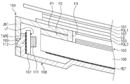
도 2는 도 1b에 도시된 도면을 설명하기 위한 확대도이다.
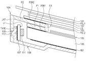
도 3은 본 발명의 다른 일 실시예의 표시 장치를 설명하기 위한 확대 단면도이다.
도 4는 본 발명의 다른 일 실시예의 표시 장치를 설명하기 위한 확대 단면도이다.
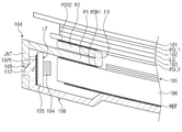
도 5는 본 발명의 다른 일 실시예의 표시 장치를 설명하기 위한 확대 단면도이다.
도 6는 본 발명의 다른 일 실시예의 표시 장치를 설명하기 위한 확대 단면도이다.
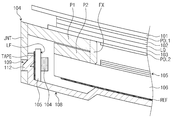
도 7는 본 발명의 다른 일 실시예의 표시 장치를 설명하기 위한 확대 단면도이다.
도 8은 본 발명의 일 실시예에 따른 표시 장치의 제조 방법의 순서도이다.
FX: 연결부 106: 도광판
104: 미들 샤시 108: 바텀 샤시
Claims (20)
- 광원;
상기 광원과 대향하는 입광면을 구비하는 도광판;
상기 도광판 상에 배치되는 미들 샤시; 및
상기 미들 샤시 상에 배치되는 표시 패널을 포함하고,
상기 미들 샤시는 제1 부, 상기 제1 부의 일단으로부터 연장되는 연결부, 및 상기 연결부로부터 연장되고 상기 제1 부의 적어도 일부분과 수직 방향으로 소정 간격 이격되고, 상기 수직 방향으로 중첩되는 제2 부를 포함하는 것을 특징으로 하는 표시 장치.
- 제1 항에 있어서,
상기 연결부는 상기 제1 부와 상기 제2 부 사이에 정의되는 만곡 기준선을 중심으로 휘어지는 것을 특징으로 하는 표시 장치.
- 제2 항에 있어서,
상기 광원은 상기 도광판의 일측에 배치되고,
상기 제1 부는 상기 광원과 상기 수직 방향으로 중첩되고, 상기 제2 부는 평면상으로 상기 광원과 이격된 것을 특징으로 하는 표시 장치.
- 제3 항에 있어서,
상기 광원이 실장되는 실장면을 포함하는 회로기판을 더 포함하고,
상기 제2 부는 일단은 상기 연결부에 연결되고, 평면상으로 보았을 때, 상기 제2 부의 타단은 상기 입광면으로부터 상기 수직 방향으로 연장되는 제1 가상면과 상기 실장면으로부터 상기 수직 방향으로 연장되는 제2 가상면 사이에 배치되는 것을 특징으로 하는 표시 장치.
- 제1 항에 있어서,
제1 접착 테이프 및 제2 접착 테이프를 더 포함하고,
상기 제1 부는 상기 제2 부의 상측에 배치되며,
상기 제1 접착 테이프의 일면은 상기 도광판에 부착되고, 상기 제1 접착 테이프의 타면은 상기 제2 부에 부착되고,
상기 제2 접착 테이프의 일면은 상기 표시 패널에 부착되고, 상기 제2 접착 테이프의 타면은 상기 제1 부에 부착되는 것을 특징으로 하는 표시 장치.
- 제1 항에 있어서,
상기 미들 샤시는 상기 제2 부로부터 연장되고 상기 제1 및 제2 부와 상기 수직 방향으로 중첩되는 제3 부를 더 포함하는 것을 특징으로 하는 표시 장치.
- 제6 항에 있어서,
상기 제2 부는 상기 제1 및 제3 부 사이에 개재되는 것을 특징으로 하는 표시 장치.
- 제7 항에 있어서,
상기 제1 부와 상기 제2 부를 연결하는 제1 연결부, 및 상기 제2 부와 상기 제3 부를 연결하는 제2 연결부를 더 포함하며,
상기 제1 연결부는 상기 제1 부와 상기 제2 부 사이에 정의되는 제1 기준선을 중심으로 휘어지고,
상기 제2 연결부는 상기 제2 부와 상기 제3 부 사이에 정의되는 제2 기준선을 중심으로 휘어지는 것을 특징으로 하는 표시 장치.
- 제1 항에 있어서,
상기 도광판 및 상기 광원을 수납하는 수납공간이 정의된 바텀 샤시를 더 포함하고,
상기 미들 샤시는 상기 제1 부의 타단으로부터 연장되고, 상기 바텀 샤시와 체결되는 체결부를 더 포함하는 것을 특징으로 하는 표시 장치.
- 제9 항에 있어서,
상기 체결부는 제1 체결부 및 상기 제1 체결부로부터 연장되며, 상기 제1 체결부의 적어도 일부분과 수평방향으로 중첩되는 제2 체결부를 포함하며,
상기 바텀 샤시는 제3 체결부 및 상기 제3 체결부로부터 연장되며, 상기 제3 체결부의 적어도 일부분과 상기 수평 방향으로 중첩되는 제4 체결부를 포함하며,
상기 제2 체결부는 상기 제4 체결부와 체결되는 것을 특징으로 하는 표시 장치.
- 제10 항에 있어서,
상기 광원이 실장되는 회로기판을 더 포함하며,
상기 회로기판은 상기 제3 체결부에 결합되는 것을 특징으로 하는 표시 장치.
- 제9 항에 있어서,
상기 제1 부의 두께와 상기 체결부의 두께는 서로 상이한 것을 특징으로 하는 표시 장치.
- 광원;
상기 광원과 대향하는 입광면을 구비하는 도광판;
상기 도광판 및 상기 광원을 수납하는 수납공간이 정의된 바텀 샤시; 및
상기 도광판 상에 배치되는 미들 샤시를 포함하고,
상기 미들 샤시는 제1 부, 상기 제1 부의 일단으로부터 연장되는 연결부, 상기 연결부로부터 연장되고 상기 제1 부의 적어도 일부분과 수직 방향으로 소정 간격 이격되고, 상기 수직 방향으로 중첩되는 제2 부, 및 상기 제1 부의 타측으로부터 연장되고, 상기 바텀 샤시와 체결되는 체결부를 포함하는 것을 특징으로 하는 백라이트 유닛.
- 제13 항에 있어서,
접착 테이프를 더 포함하며,
상기 제1 부는 상기 제2 부의 상측에 배치되며,
상기 접착 테이프의 일면은 상기 도광판에 부착되고, 상기 접착 테이프의 타면은 상기 제2 부에 부착되는 것을 특징으로 하는 백라이트 유닛.
- 제13 항에 있어서,
접착 테이프를 더 포함하며,
상기 제1 부는 상기 제2 부의 하측에 배치되며,
상기 접착 테이프의 일면은 상기 도광판에 부착되고, 상기 접착 테이프의 타면은 상기 제1 부에 부착되는 것을 특징으로 하는 백라이트 유닛.
- 제13 항에 있어서,
복수의 광학 시트를 더 포함하며,
상기 복수의 광학 시트는 상기 도광판 상측에 배치되고, 상기 제1 부 및 상기 제2 부와 평면상으로 보았을 때 이격되는 것을 특징으로 하는 백라이트 유닛.
- 제13 항에 있어서,
상기 미들 샤시는 상기 제2 부로부터 연장되고 상기 제1 및 제2 부와 상기 수직 방향으로 중첩되는 제3 부를 더 포함하는 것을 특징으로 하는 백라이트 유닛.
- 샤시 부재를 제공하는 단계;
상기 샤시 부재로부터 미들 샤시를 제작하는 단계; 및
상기 미들 샤시가 도광판의 일단 및 표시 패널의 일단과 수직 방향으로 중첩하도록 상기 도광판 및 상기 표시 패널을 상기 미들 샤시와 결합 시키는 단계를 포함하고,
상기 미들 샤시를 제작하는 단계는 상기 샤시 부재의 제1 및 제2 부가 상기 수직 방향으로 중첩되도록, 상기 제1 부 및 상기 제2 부를 연결하는 제1 연결부를 구부리는 단계를 포함하는 표시 장치 제조 방법.
- 제18 항에 있어서,
상기 제1 부가 상기 제2 부의 상측에 배치되고,
상기 미들 샤시와 결합 시키는 단계는
제1 접착 테이프의 일면은 도광판에 부착시키고, 상기 제1 접착 테이프의 타면은 상기 제2 부에 부착시키는 단계; 및
상기 제2 접착 테이프의 일면은 표시 패널에 부착시키고, 상기 제2 접착 테이프의 타면은 상기 제1 부에 부착시키는 단계를 포함하는 것을 특징으로 하는 표시 장치 제조 방법.
- 제18 항에 있어서,
상기 미들 샤시를 제작하는 단계는 제3 부가 상기 제1 부 및 상기 제2 부와 상기 수직방향으로 중첩되도록 상기 제2 부와 상기 제3 부를 연결하는 제2 연결부를 구부리는 단계를 더 포함하는 표시 장치 제조 방법.
Priority Applications (4)
| Application Number | Priority Date | Filing Date | Title |
|---|---|---|---|
| KR1020150154074A KR102451998B1 (ko) | 2015-11-03 | 2015-11-03 | 표시장치 및 이의 제조 방법 |
| US15/196,204 US10254470B2 (en) | 2015-11-03 | 2016-06-29 | Display device and method of manufacturing the same |
| CN201610957929.2A CN106842693B (zh) | 2015-11-03 | 2016-10-27 | 背光单元、显示设备及其制造方法 |
| US15/977,524 US20180259704A1 (en) | 2015-11-03 | 2018-05-11 | Display device |
Applications Claiming Priority (1)
| Application Number | Priority Date | Filing Date | Title |
|---|---|---|---|
| KR1020150154074A KR102451998B1 (ko) | 2015-11-03 | 2015-11-03 | 표시장치 및 이의 제조 방법 |
Publications (2)
| Publication Number | Publication Date |
|---|---|
| KR20170052760A true KR20170052760A (ko) | 2017-05-15 |
| KR102451998B1 KR102451998B1 (ko) | 2022-10-11 |
Family
ID=58634509
Family Applications (1)
| Application Number | Title | Priority Date | Filing Date |
|---|---|---|---|
| KR1020150154074A Active KR102451998B1 (ko) | 2015-11-03 | 2015-11-03 | 표시장치 및 이의 제조 방법 |
Country Status (3)
| Country | Link |
|---|---|
| US (1) | US10254470B2 (ko) |
| KR (1) | KR102451998B1 (ko) |
| CN (1) | CN106842693B (ko) |
Cited By (1)
| Publication number | Priority date | Publication date | Assignee | Title |
|---|---|---|---|---|
| KR20190108665A (ko) * | 2018-03-14 | 2019-09-25 | 삼성디스플레이 주식회사 | 표시 모듈 및 이를 포함하는 표시 장치 |
Families Citing this family (14)
| Publication number | Priority date | Publication date | Assignee | Title |
|---|---|---|---|---|
| JP6517724B2 (ja) * | 2016-04-08 | 2019-05-22 | ミネベアミツミ株式会社 | 面状照明装置 |
| KR101866314B1 (ko) * | 2016-07-12 | 2018-06-12 | (주)코텍 | 곡면형 디스플레이 |
| CN107390416A (zh) * | 2017-09-19 | 2017-11-24 | 合肥惠科金扬科技有限公司 | 显示模组、显示屏及电子产品 |
| KR20190034368A (ko) * | 2017-09-22 | 2019-04-02 | 삼성디스플레이 주식회사 | 백라이트 유닛 및 이를 포함하는 표시 장치 |
| TWM557369U (zh) * | 2017-11-09 | 2018-03-21 | 揚昇照明股份有限公司 | 反射式顯示裝置 |
| KR20190079727A (ko) * | 2017-12-27 | 2019-07-08 | 삼성디스플레이 주식회사 | 표시 장치 |
| CN110646963A (zh) * | 2018-06-26 | 2020-01-03 | 鸿富锦精密工业(深圳)有限公司 | 液晶显示模组及显示装置 |
| CN110646964A (zh) * | 2018-06-27 | 2020-01-03 | 夏普株式会社 | 液晶显示装置 |
| CN110673252B (zh) * | 2019-09-12 | 2021-09-03 | 惠州市华星光电技术有限公司 | 导光板及其显示装置 |
| WO2024065479A1 (zh) * | 2022-09-29 | 2024-04-04 | 京东方科技集团股份有限公司 | 背光模组、显示装置及触控显示装置 |
| CN120233573A (zh) * | 2023-12-29 | 2025-07-01 | 海信视像科技股份有限公司 | 显示装置 |
| CN120233571A (zh) * | 2023-12-29 | 2025-07-01 | 海信视像科技股份有限公司 | 显示装置 |
| WO2025139089A1 (zh) * | 2023-12-29 | 2025-07-03 | 海信视像科技股份有限公司 | 显示装置及背板的制备方法 |
| CN120233572A (zh) * | 2023-12-29 | 2025-07-01 | 海信视像科技股份有限公司 | 显示装置 |
Citations (3)
| Publication number | Priority date | Publication date | Assignee | Title |
|---|---|---|---|---|
| JP2012118498A (ja) * | 2010-12-03 | 2012-06-21 | Wistron Corp | フラットパネルディスプレイ |
| JP2012198434A (ja) * | 2011-03-22 | 2012-10-18 | Japan Display East Co Ltd | 液晶表示装置 |
| KR20150092408A (ko) * | 2014-02-04 | 2015-08-13 | 삼성디스플레이 주식회사 | 커브드 백라이트 어셈블리 및 이를 갖는 커브드 표시장치 |
Family Cites Families (16)
| Publication number | Priority date | Publication date | Assignee | Title |
|---|---|---|---|---|
| JP3511591B2 (ja) * | 1999-07-05 | 2004-03-29 | 株式会社アドバンスト・ディスプレイ | 液晶表示装置 |
| JP2003346535A (ja) * | 2002-03-20 | 2003-12-05 | Advanced Display Inc | 面状光源装置及び表示装置 |
| US7153018B2 (en) * | 2002-09-19 | 2006-12-26 | Matsushita Electric Industrial Co., Ltd. | Illumination unit and liquid crystal display comprising it |
| TWI348055B (en) * | 2005-10-18 | 2011-09-01 | Coretronic Corp | Plane light source apparatus |
| WO2008090646A1 (ja) * | 2007-01-22 | 2008-07-31 | Sharp Kabushiki Kaisha | バックライト装置、およびそれを用いた平面表示装置 |
| KR101014464B1 (ko) * | 2009-01-13 | 2011-02-14 | 엘지디스플레이 주식회사 | 액정표시장치 |
| JP5394492B2 (ja) * | 2009-07-29 | 2014-01-22 | アルプス電気株式会社 | 操作装置 |
| US9032371B2 (en) * | 2010-11-21 | 2015-05-12 | Verifyter Ab | Method and apparatus for automatic diagnosis of software failures |
| KR101926430B1 (ko) * | 2011-04-18 | 2018-12-10 | 엘지디스플레이 주식회사 | 디스플레이 장치 |
| JP2013003487A (ja) | 2011-06-21 | 2013-01-07 | Panasonic Liquid Crystal Display Co Ltd | 表示装置 |
| KR101909436B1 (ko) | 2012-08-10 | 2018-10-18 | 엘지디스플레이 주식회사 | 디스플레이 장치 및 그의 제조 방법 |
| TWI464501B (zh) * | 2012-08-28 | 2014-12-11 | Au Optronics Corp | 結構支架及面板顯示模組 |
| KR101966739B1 (ko) | 2012-11-09 | 2019-04-09 | 삼성전자주식회사 | 곡면 디스플레이 장치 |
| KR101472752B1 (ko) * | 2012-12-24 | 2014-12-15 | 엘지디스플레이 주식회사 | 액정표시장치 |
| KR102232166B1 (ko) * | 2014-03-06 | 2021-03-29 | 삼성디스플레이 주식회사 | 표시 장치 |
| US10371887B2 (en) * | 2014-09-26 | 2019-08-06 | Sakai Display Products Corporation | Display apparatus with U-shaped coupling member |
-
2015
- 2015-11-03 KR KR1020150154074A patent/KR102451998B1/ko active Active
-
2016
- 2016-06-29 US US15/196,204 patent/US10254470B2/en active Active
- 2016-10-27 CN CN201610957929.2A patent/CN106842693B/zh active Active
Patent Citations (3)
| Publication number | Priority date | Publication date | Assignee | Title |
|---|---|---|---|---|
| JP2012118498A (ja) * | 2010-12-03 | 2012-06-21 | Wistron Corp | フラットパネルディスプレイ |
| JP2012198434A (ja) * | 2011-03-22 | 2012-10-18 | Japan Display East Co Ltd | 液晶表示装置 |
| KR20150092408A (ko) * | 2014-02-04 | 2015-08-13 | 삼성디스플레이 주식회사 | 커브드 백라이트 어셈블리 및 이를 갖는 커브드 표시장치 |
Cited By (1)
| Publication number | Priority date | Publication date | Assignee | Title |
|---|---|---|---|---|
| KR20190108665A (ko) * | 2018-03-14 | 2019-09-25 | 삼성디스플레이 주식회사 | 표시 모듈 및 이를 포함하는 표시 장치 |
Also Published As
| Publication number | Publication date |
|---|---|
| KR102451998B1 (ko) | 2022-10-11 |
| CN106842693A (zh) | 2017-06-13 |
| US10254470B2 (en) | 2019-04-09 |
| CN106842693B (zh) | 2021-08-27 |
| US20170123144A1 (en) | 2017-05-04 |
Similar Documents
| Publication | Publication Date | Title |
|---|---|---|
| KR102451998B1 (ko) | 표시장치 및 이의 제조 방법 | |
| US8531624B2 (en) | LCD device | |
| US8134658B2 (en) | Liquid crystal display module | |
| KR100759736B1 (ko) | 액정 디스플레이 장치 | |
| US9291853B2 (en) | Display device | |
| US9467641B2 (en) | Television and electronic apparatus | |
| US20100020261A1 (en) | Liquid crystal display device | |
| US20070252922A1 (en) | Liquid crystal display device | |
| US9025104B2 (en) | Backboard structure, backlight module, liquid crystal display module | |
| EP2153273B1 (en) | Display device | |
| CN102193219B (zh) | 显示装置及其组装方法 | |
| KR102237372B1 (ko) | 연결 홀더 및 그를 포함하는 표시장치 | |
| US8780293B2 (en) | Liquid crystal display device, backlight module and frame unit thereof | |
| KR20180067797A (ko) | 전자 기기 | |
| US20130077343A1 (en) | Backlight unit and display apparatus having the same | |
| US10345510B2 (en) | Liquid crystal display | |
| CN104823101A (zh) | 液晶显示装置 | |
| JP7064264B2 (ja) | 表示装置 | |
| EP2755079A2 (en) | Display apparatus | |
| US10139544B2 (en) | Light guide plate, back plate, edge-lit type backlight module and display device | |
| KR101693045B1 (ko) | 액정표시장치 | |
| US9341876B2 (en) | Liquid crystal display device | |
| KR20180071614A (ko) | 액정표시장치 | |
| US9164304B2 (en) | Liquid crystal display assembly and electronic device | |
| US9395567B2 (en) | Display device and liquid crystal display device that prevent cracking of a display panel without increasing in size |
Legal Events
| Date | Code | Title | Description |
|---|---|---|---|
| PA0109 | Patent application |
Patent event code: PA01091R01D Comment text: Patent Application Patent event date: 20151103 |
|
| PG1501 | Laying open of application | ||
| A201 | Request for examination | ||
| PA0201 | Request for examination |
Patent event code: PA02012R01D Patent event date: 20201029 Comment text: Request for Examination of Application Patent event code: PA02011R01I Patent event date: 20151103 Comment text: Patent Application |
|
| E902 | Notification of reason for refusal | ||
| PE0902 | Notice of grounds for rejection |
Comment text: Notification of reason for refusal Patent event date: 20220119 Patent event code: PE09021S01D |
|
| E701 | Decision to grant or registration of patent right | ||
| PE0701 | Decision of registration |
Patent event code: PE07011S01D Comment text: Decision to Grant Registration Patent event date: 20220705 |
|
| GRNT | Written decision to grant | ||
| PR0701 | Registration of establishment |
Comment text: Registration of Establishment Patent event date: 20221004 Patent event code: PR07011E01D |
|
| PR1002 | Payment of registration fee |
Payment date: 20221005 End annual number: 3 Start annual number: 1 |
|
| PG1601 | Publication of registration |