KR20170052801A - 표시 장치 및 그 제조 방법 - Google Patents
표시 장치 및 그 제조 방법 Download PDFInfo
- Publication number
- KR20170052801A KR20170052801A KR1020150154552A KR20150154552A KR20170052801A KR 20170052801 A KR20170052801 A KR 20170052801A KR 1020150154552 A KR1020150154552 A KR 1020150154552A KR 20150154552 A KR20150154552 A KR 20150154552A KR 20170052801 A KR20170052801 A KR 20170052801A
- Authority
- KR
- South Korea
- Prior art keywords
- reflective layer
- color filter
- thin film
- disposed
- film transistor
- Prior art date
- Legal status (The legal status is an assumption and is not a legal conclusion. Google has not performed a legal analysis and makes no representation as to the accuracy of the status listed.)
- Granted
Links
Images









Classifications
-
- G—PHYSICS
- G02—OPTICS
- G02F—OPTICAL DEVICES OR ARRANGEMENTS FOR THE CONTROL OF LIGHT BY MODIFICATION OF THE OPTICAL PROPERTIES OF THE MEDIA OF THE ELEMENTS INVOLVED THEREIN; NON-LINEAR OPTICS; FREQUENCY-CHANGING OF LIGHT; OPTICAL LOGIC ELEMENTS; OPTICAL ANALOGUE/DIGITAL CONVERTERS
- G02F1/00—Devices or arrangements for the control of the intensity, colour, phase, polarisation or direction of light arriving from an independent light source, e.g. switching, gating or modulating; Non-linear optics
- G02F1/01—Devices or arrangements for the control of the intensity, colour, phase, polarisation or direction of light arriving from an independent light source, e.g. switching, gating or modulating; Non-linear optics for the control of the intensity, phase, polarisation or colour
- G02F1/13—Devices or arrangements for the control of the intensity, colour, phase, polarisation or direction of light arriving from an independent light source, e.g. switching, gating or modulating; Non-linear optics for the control of the intensity, phase, polarisation or colour based on liquid crystals, e.g. single liquid crystal display cells
- G02F1/133—Constructional arrangements; Operation of liquid crystal cells; Circuit arrangements
- G02F1/136—Liquid crystal cells structurally associated with a semi-conducting layer or substrate, e.g. cells forming part of an integrated circuit
- G02F1/1362—Active matrix addressed cells
- G02F1/1368—Active matrix addressed cells in which the switching element is a three-electrode device
-
- G—PHYSICS
- G02—OPTICS
- G02F—OPTICAL DEVICES OR ARRANGEMENTS FOR THE CONTROL OF LIGHT BY MODIFICATION OF THE OPTICAL PROPERTIES OF THE MEDIA OF THE ELEMENTS INVOLVED THEREIN; NON-LINEAR OPTICS; FREQUENCY-CHANGING OF LIGHT; OPTICAL LOGIC ELEMENTS; OPTICAL ANALOGUE/DIGITAL CONVERTERS
- G02F1/00—Devices or arrangements for the control of the intensity, colour, phase, polarisation or direction of light arriving from an independent light source, e.g. switching, gating or modulating; Non-linear optics
- G02F1/01—Devices or arrangements for the control of the intensity, colour, phase, polarisation or direction of light arriving from an independent light source, e.g. switching, gating or modulating; Non-linear optics for the control of the intensity, phase, polarisation or colour
- G02F1/13—Devices or arrangements for the control of the intensity, colour, phase, polarisation or direction of light arriving from an independent light source, e.g. switching, gating or modulating; Non-linear optics for the control of the intensity, phase, polarisation or colour based on liquid crystals, e.g. single liquid crystal display cells
- G02F1/133—Constructional arrangements; Operation of liquid crystal cells; Circuit arrangements
- G02F1/1333—Constructional arrangements; Manufacturing methods
- G02F1/1335—Structural association of cells with optical devices, e.g. polarisers or reflectors
- G02F1/133509—Filters, e.g. light shielding masks
- G02F1/133514—Colour filters
- G02F1/133516—Methods for their manufacture, e.g. printing, electro-deposition or photolithography
-
- G—PHYSICS
- G02—OPTICS
- G02F—OPTICAL DEVICES OR ARRANGEMENTS FOR THE CONTROL OF LIGHT BY MODIFICATION OF THE OPTICAL PROPERTIES OF THE MEDIA OF THE ELEMENTS INVOLVED THEREIN; NON-LINEAR OPTICS; FREQUENCY-CHANGING OF LIGHT; OPTICAL LOGIC ELEMENTS; OPTICAL ANALOGUE/DIGITAL CONVERTERS
- G02F1/00—Devices or arrangements for the control of the intensity, colour, phase, polarisation or direction of light arriving from an independent light source, e.g. switching, gating or modulating; Non-linear optics
- G02F1/01—Devices or arrangements for the control of the intensity, colour, phase, polarisation or direction of light arriving from an independent light source, e.g. switching, gating or modulating; Non-linear optics for the control of the intensity, phase, polarisation or colour
- G02F1/13—Devices or arrangements for the control of the intensity, colour, phase, polarisation or direction of light arriving from an independent light source, e.g. switching, gating or modulating; Non-linear optics for the control of the intensity, phase, polarisation or colour based on liquid crystals, e.g. single liquid crystal display cells
- G02F1/133—Constructional arrangements; Operation of liquid crystal cells; Circuit arrangements
- G02F1/1333—Constructional arrangements; Manufacturing methods
- G02F1/133345—Insulating layers
-
- G—PHYSICS
- G02—OPTICS
- G02F—OPTICAL DEVICES OR ARRANGEMENTS FOR THE CONTROL OF LIGHT BY MODIFICATION OF THE OPTICAL PROPERTIES OF THE MEDIA OF THE ELEMENTS INVOLVED THEREIN; NON-LINEAR OPTICS; FREQUENCY-CHANGING OF LIGHT; OPTICAL LOGIC ELEMENTS; OPTICAL ANALOGUE/DIGITAL CONVERTERS
- G02F1/00—Devices or arrangements for the control of the intensity, colour, phase, polarisation or direction of light arriving from an independent light source, e.g. switching, gating or modulating; Non-linear optics
- G02F1/01—Devices or arrangements for the control of the intensity, colour, phase, polarisation or direction of light arriving from an independent light source, e.g. switching, gating or modulating; Non-linear optics for the control of the intensity, phase, polarisation or colour
- G02F1/13—Devices or arrangements for the control of the intensity, colour, phase, polarisation or direction of light arriving from an independent light source, e.g. switching, gating or modulating; Non-linear optics for the control of the intensity, phase, polarisation or colour based on liquid crystals, e.g. single liquid crystal display cells
- G02F1/133—Constructional arrangements; Operation of liquid crystal cells; Circuit arrangements
- G02F1/1333—Constructional arrangements; Manufacturing methods
- G02F1/1335—Structural association of cells with optical devices, e.g. polarisers or reflectors
- G02F1/133509—Filters, e.g. light shielding masks
- G02F1/133512—Light shielding layers, e.g. black matrix
-
- G—PHYSICS
- G02—OPTICS
- G02F—OPTICAL DEVICES OR ARRANGEMENTS FOR THE CONTROL OF LIGHT BY MODIFICATION OF THE OPTICAL PROPERTIES OF THE MEDIA OF THE ELEMENTS INVOLVED THEREIN; NON-LINEAR OPTICS; FREQUENCY-CHANGING OF LIGHT; OPTICAL LOGIC ELEMENTS; OPTICAL ANALOGUE/DIGITAL CONVERTERS
- G02F1/00—Devices or arrangements for the control of the intensity, colour, phase, polarisation or direction of light arriving from an independent light source, e.g. switching, gating or modulating; Non-linear optics
- G02F1/01—Devices or arrangements for the control of the intensity, colour, phase, polarisation or direction of light arriving from an independent light source, e.g. switching, gating or modulating; Non-linear optics for the control of the intensity, phase, polarisation or colour
- G02F1/13—Devices or arrangements for the control of the intensity, colour, phase, polarisation or direction of light arriving from an independent light source, e.g. switching, gating or modulating; Non-linear optics for the control of the intensity, phase, polarisation or colour based on liquid crystals, e.g. single liquid crystal display cells
- G02F1/133—Constructional arrangements; Operation of liquid crystal cells; Circuit arrangements
- G02F1/1333—Constructional arrangements; Manufacturing methods
- G02F1/1335—Structural association of cells with optical devices, e.g. polarisers or reflectors
- G02F1/133509—Filters, e.g. light shielding masks
- G02F1/133514—Colour filters
-
- G—PHYSICS
- G02—OPTICS
- G02F—OPTICAL DEVICES OR ARRANGEMENTS FOR THE CONTROL OF LIGHT BY MODIFICATION OF THE OPTICAL PROPERTIES OF THE MEDIA OF THE ELEMENTS INVOLVED THEREIN; NON-LINEAR OPTICS; FREQUENCY-CHANGING OF LIGHT; OPTICAL LOGIC ELEMENTS; OPTICAL ANALOGUE/DIGITAL CONVERTERS
- G02F1/00—Devices or arrangements for the control of the intensity, colour, phase, polarisation or direction of light arriving from an independent light source, e.g. switching, gating or modulating; Non-linear optics
- G02F1/01—Devices or arrangements for the control of the intensity, colour, phase, polarisation or direction of light arriving from an independent light source, e.g. switching, gating or modulating; Non-linear optics for the control of the intensity, phase, polarisation or colour
- G02F1/13—Devices or arrangements for the control of the intensity, colour, phase, polarisation or direction of light arriving from an independent light source, e.g. switching, gating or modulating; Non-linear optics for the control of the intensity, phase, polarisation or colour based on liquid crystals, e.g. single liquid crystal display cells
- G02F1/133—Constructional arrangements; Operation of liquid crystal cells; Circuit arrangements
- G02F1/1333—Constructional arrangements; Manufacturing methods
- G02F1/1335—Structural association of cells with optical devices, e.g. polarisers or reflectors
- G02F1/133553—Reflecting elements
-
- G—PHYSICS
- G09—EDUCATION; CRYPTOGRAPHY; DISPLAY; ADVERTISING; SEALS
- G09G—ARRANGEMENTS OR CIRCUITS FOR CONTROL OF INDICATING DEVICES USING STATIC MEANS TO PRESENT VARIABLE INFORMATION
- G09G3/00—Control arrangements or circuits, of interest only in connection with visual indicators other than cathode-ray tubes
- G09G3/20—Control arrangements or circuits, of interest only in connection with visual indicators other than cathode-ray tubes for presentation of an assembly of a number of characters, e.g. a page, by composing the assembly by combination of individual elements arranged in a matrix no fixed position being assigned to or needed to be assigned to the individual characters or partial characters
- G09G3/34—Control arrangements or circuits, of interest only in connection with visual indicators other than cathode-ray tubes for presentation of an assembly of a number of characters, e.g. a page, by composing the assembly by combination of individual elements arranged in a matrix no fixed position being assigned to or needed to be assigned to the individual characters or partial characters by control of light from an independent source
- G09G3/36—Control arrangements or circuits, of interest only in connection with visual indicators other than cathode-ray tubes for presentation of an assembly of a number of characters, e.g. a page, by composing the assembly by combination of individual elements arranged in a matrix no fixed position being assigned to or needed to be assigned to the individual characters or partial characters by control of light from an independent source using liquid crystals
-
- H01L29/786—
-
- H—ELECTRICITY
- H10—SEMICONDUCTOR DEVICES; ELECTRIC SOLID-STATE DEVICES NOT OTHERWISE PROVIDED FOR
- H10D—INORGANIC ELECTRIC SEMICONDUCTOR DEVICES
- H10D30/00—Field-effect transistors [FET]
- H10D30/60—Insulated-gate field-effect transistors [IGFET]
- H10D30/67—Thin-film transistors [TFT]
- H10D30/6704—Thin-film transistors [TFT] having supplementary regions or layers in the thin films or in the insulated bulk substrates for controlling properties of the device
- H10D30/6713—Thin-film transistors [TFT] having supplementary regions or layers in the thin films or in the insulated bulk substrates for controlling properties of the device characterised by the properties of the source or drain regions, e.g. compositions or sectional shapes
-
- H—ELECTRICITY
- H10—SEMICONDUCTOR DEVICES; ELECTRIC SOLID-STATE DEVICES NOT OTHERWISE PROVIDED FOR
- H10D—INORGANIC ELECTRIC SEMICONDUCTOR DEVICES
- H10D30/00—Field-effect transistors [FET]
- H10D30/60—Insulated-gate field-effect transistors [IGFET]
- H10D30/67—Thin-film transistors [TFT]
- H10D30/6704—Thin-film transistors [TFT] having supplementary regions or layers in the thin films or in the insulated bulk substrates for controlling properties of the device
- H10D30/6723—Thin-film transistors [TFT] having supplementary regions or layers in the thin films or in the insulated bulk substrates for controlling properties of the device having light shields
-
- H—ELECTRICITY
- H10—SEMICONDUCTOR DEVICES; ELECTRIC SOLID-STATE DEVICES NOT OTHERWISE PROVIDED FOR
- H10D—INORGANIC ELECTRIC SEMICONDUCTOR DEVICES
- H10D30/00—Field-effect transistors [FET]
- H10D30/60—Insulated-gate field-effect transistors [IGFET]
- H10D30/67—Thin-film transistors [TFT]
- H10D30/6729—Thin-film transistors [TFT] characterised by the electrodes
- H10D30/673—Thin-film transistors [TFT] characterised by the electrodes characterised by the shapes, relative sizes or dispositions of the gate electrodes
- H10D30/6732—Bottom-gate only TFTs
-
- H—ELECTRICITY
- H10—SEMICONDUCTOR DEVICES; ELECTRIC SOLID-STATE DEVICES NOT OTHERWISE PROVIDED FOR
- H10D—INORGANIC ELECTRIC SEMICONDUCTOR DEVICES
- H10D30/00—Field-effect transistors [FET]
- H10D30/60—Insulated-gate field-effect transistors [IGFET]
- H10D30/67—Thin-film transistors [TFT]
- H10D30/674—Thin-film transistors [TFT] characterised by the active materials
- H10D30/6741—Group IV materials, e.g. germanium or silicon carbide
- H10D30/6743—Silicon
- H10D30/6746—Amorphous silicon
-
- H—ELECTRICITY
- H10—SEMICONDUCTOR DEVICES; ELECTRIC SOLID-STATE DEVICES NOT OTHERWISE PROVIDED FOR
- H10D—INORGANIC ELECTRIC SEMICONDUCTOR DEVICES
- H10D86/00—Integrated devices formed in or on insulating or conducting substrates, e.g. formed in silicon-on-insulator [SOI] substrates or on stainless steel or glass substrates
- H10D86/01—Manufacture or treatment
- H10D86/021—Manufacture or treatment of multiple TFTs
- H10D86/0212—Manufacture or treatment of multiple TFTs comprising manufacture, treatment or coating of substrates
-
- H—ELECTRICITY
- H10—SEMICONDUCTOR DEVICES; ELECTRIC SOLID-STATE DEVICES NOT OTHERWISE PROVIDED FOR
- H10D—INORGANIC ELECTRIC SEMICONDUCTOR DEVICES
- H10D86/00—Integrated devices formed in or on insulating or conducting substrates, e.g. formed in silicon-on-insulator [SOI] substrates or on stainless steel or glass substrates
- H10D86/40—Integrated devices formed in or on insulating or conducting substrates, e.g. formed in silicon-on-insulator [SOI] substrates or on stainless steel or glass substrates characterised by multiple TFTs
- H10D86/421—Integrated devices formed in or on insulating or conducting substrates, e.g. formed in silicon-on-insulator [SOI] substrates or on stainless steel or glass substrates characterised by multiple TFTs having a particular composition, shape or crystalline structure of the active layer
-
- H—ELECTRICITY
- H10—SEMICONDUCTOR DEVICES; ELECTRIC SOLID-STATE DEVICES NOT OTHERWISE PROVIDED FOR
- H10D—INORGANIC ELECTRIC SEMICONDUCTOR DEVICES
- H10D86/00—Integrated devices formed in or on insulating or conducting substrates, e.g. formed in silicon-on-insulator [SOI] substrates or on stainless steel or glass substrates
- H10D86/40—Integrated devices formed in or on insulating or conducting substrates, e.g. formed in silicon-on-insulator [SOI] substrates or on stainless steel or glass substrates characterised by multiple TFTs
- H10D86/441—Interconnections, e.g. scanning lines
-
- H—ELECTRICITY
- H10—SEMICONDUCTOR DEVICES; ELECTRIC SOLID-STATE DEVICES NOT OTHERWISE PROVIDED FOR
- H10D—INORGANIC ELECTRIC SEMICONDUCTOR DEVICES
- H10D86/00—Integrated devices formed in or on insulating or conducting substrates, e.g. formed in silicon-on-insulator [SOI] substrates or on stainless steel or glass substrates
- H10D86/40—Integrated devices formed in or on insulating or conducting substrates, e.g. formed in silicon-on-insulator [SOI] substrates or on stainless steel or glass substrates characterised by multiple TFTs
- H10D86/451—Integrated devices formed in or on insulating or conducting substrates, e.g. formed in silicon-on-insulator [SOI] substrates or on stainless steel or glass substrates characterised by multiple TFTs characterised by the compositions or shapes of the interlayer dielectrics
-
- H—ELECTRICITY
- H10—SEMICONDUCTOR DEVICES; ELECTRIC SOLID-STATE DEVICES NOT OTHERWISE PROVIDED FOR
- H10D—INORGANIC ELECTRIC SEMICONDUCTOR DEVICES
- H10D86/00—Integrated devices formed in or on insulating or conducting substrates, e.g. formed in silicon-on-insulator [SOI] substrates or on stainless steel or glass substrates
- H10D86/40—Integrated devices formed in or on insulating or conducting substrates, e.g. formed in silicon-on-insulator [SOI] substrates or on stainless steel or glass substrates characterised by multiple TFTs
- H10D86/60—Integrated devices formed in or on insulating or conducting substrates, e.g. formed in silicon-on-insulator [SOI] substrates or on stainless steel or glass substrates characterised by multiple TFTs wherein the TFTs are in active matrices
-
- G—PHYSICS
- G02—OPTICS
- G02F—OPTICAL DEVICES OR ARRANGEMENTS FOR THE CONTROL OF LIGHT BY MODIFICATION OF THE OPTICAL PROPERTIES OF THE MEDIA OF THE ELEMENTS INVOLVED THEREIN; NON-LINEAR OPTICS; FREQUENCY-CHANGING OF LIGHT; OPTICAL LOGIC ELEMENTS; OPTICAL ANALOGUE/DIGITAL CONVERTERS
- G02F1/00—Devices or arrangements for the control of the intensity, colour, phase, polarisation or direction of light arriving from an independent light source, e.g. switching, gating or modulating; Non-linear optics
- G02F1/01—Devices or arrangements for the control of the intensity, colour, phase, polarisation or direction of light arriving from an independent light source, e.g. switching, gating or modulating; Non-linear optics for the control of the intensity, phase, polarisation or colour
- G02F1/13—Devices or arrangements for the control of the intensity, colour, phase, polarisation or direction of light arriving from an independent light source, e.g. switching, gating or modulating; Non-linear optics for the control of the intensity, phase, polarisation or colour based on liquid crystals, e.g. single liquid crystal display cells
- G02F1/133—Constructional arrangements; Operation of liquid crystal cells; Circuit arrangements
- G02F1/136—Liquid crystal cells structurally associated with a semi-conducting layer or substrate, e.g. cells forming part of an integrated circuit
- G02F1/1362—Active matrix addressed cells
- G02F1/136209—Light shielding layers, e.g. black matrix, incorporated in the active matrix substrate, e.g. structurally associated with the switching element
-
- G—PHYSICS
- G02—OPTICS
- G02F—OPTICAL DEVICES OR ARRANGEMENTS FOR THE CONTROL OF LIGHT BY MODIFICATION OF THE OPTICAL PROPERTIES OF THE MEDIA OF THE ELEMENTS INVOLVED THEREIN; NON-LINEAR OPTICS; FREQUENCY-CHANGING OF LIGHT; OPTICAL LOGIC ELEMENTS; OPTICAL ANALOGUE/DIGITAL CONVERTERS
- G02F1/00—Devices or arrangements for the control of the intensity, colour, phase, polarisation or direction of light arriving from an independent light source, e.g. switching, gating or modulating; Non-linear optics
- G02F1/01—Devices or arrangements for the control of the intensity, colour, phase, polarisation or direction of light arriving from an independent light source, e.g. switching, gating or modulating; Non-linear optics for the control of the intensity, phase, polarisation or colour
- G02F1/13—Devices or arrangements for the control of the intensity, colour, phase, polarisation or direction of light arriving from an independent light source, e.g. switching, gating or modulating; Non-linear optics for the control of the intensity, phase, polarisation or colour based on liquid crystals, e.g. single liquid crystal display cells
- G02F1/133—Constructional arrangements; Operation of liquid crystal cells; Circuit arrangements
- G02F1/136—Liquid crystal cells structurally associated with a semi-conducting layer or substrate, e.g. cells forming part of an integrated circuit
- G02F1/1362—Active matrix addressed cells
- G02F1/136222—Colour filters incorporated in the active matrix substrate
-
- G—PHYSICS
- G02—OPTICS
- G02F—OPTICAL DEVICES OR ARRANGEMENTS FOR THE CONTROL OF LIGHT BY MODIFICATION OF THE OPTICAL PROPERTIES OF THE MEDIA OF THE ELEMENTS INVOLVED THEREIN; NON-LINEAR OPTICS; FREQUENCY-CHANGING OF LIGHT; OPTICAL LOGIC ELEMENTS; OPTICAL ANALOGUE/DIGITAL CONVERTERS
- G02F2201/00—Constructional arrangements not provided for in groups G02F1/00 - G02F7/00
- G02F2201/12—Constructional arrangements not provided for in groups G02F1/00 - G02F7/00 electrode
- G02F2201/123—Constructional arrangements not provided for in groups G02F1/00 - G02F7/00 electrode pixel
Landscapes
- Physics & Mathematics (AREA)
- Nonlinear Science (AREA)
- Chemical & Material Sciences (AREA)
- Crystallography & Structural Chemistry (AREA)
- General Physics & Mathematics (AREA)
- Optics & Photonics (AREA)
- Mathematical Physics (AREA)
- Engineering & Computer Science (AREA)
- Liquid Crystal (AREA)
- Microelectronics & Electronic Packaging (AREA)
- Computer Hardware Design (AREA)
- Theoretical Computer Science (AREA)
- Manufacturing & Machinery (AREA)
Abstract
Description
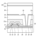
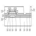
도 2는 도 1의 Ⅰ-Ⅰ'를 따라 절단한 단면도이다.
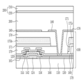
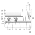
도 3은 본 발명의 다른 일실시예에 따른 표시 장치를 개략적으로 나타낸 단면도이다.
도 4는 본 발명의 다른 실시예에 따른 표시 장치를 개략적으로 나타낸 평면도이다.
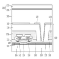
도 5 및 6은 도 4의 Ⅱ-Ⅱ'를 따라 절단한 단면도이다
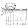
도 7a 내지 도 7e는 본 발명의 일실시예에 따른 표시 장치 제조 방법을 나타낸 단면도이다.
도 8은 본 발명의 다른 실시예에 따른 표시 장치 제조 방법을 나타낸 단면도이다.
도 9a 내지 9f는 본 발명의 다른 실시예에 따른 표시 장치의 제조 방법을 나타낸 단면도이다.
171: 반사층, 175: 색필터,
178: 제 1 절연막, 179: 제 2 절연막
Claims (15)
- 제 1 기판;
상기 제 1 기판 상에 배치되는 박막 트랜지스터;
상기 박막 트랜지스터 상에 배치되는 보호막;
상기 보호막 상에 배치되는 반사층;
상기 반사층 상에 배치되는 색필터;
상기 색필터 상에 배치되는 제 1 절연막;
상기 제 1 절연막 상에 배치되는 화소 전극; 및
상기 제 1 기판과 대향하는 제 2 기판과 상기 제 1 기판과 상기 제 2 기판 사이에 배치되는 액정층을 포함하며,
상기 반사층은 평면 상에서 색필터와 실질적으로 동일한 형상을 갖는 표시 장치.
- 제 1 항에 있어서,
상기 박막 트랜지스터 및 상기 반사층 사이에 배치되는 제 2 절연막을 더 포함하는 표시 장치.
- 제 1 항에 있어서,
상기 색필터 및 상기 반사층은 상기 박막 트랜지스터와 중첩되지 않는 표시 장치.
- 제 3 항에 있어서,
상기 제 1 절연막 상에 배치되며, 상기 박막 트랜지스터와 중첩되는 차광부재를 더 포함하는 표시 장치.
- 제 1 항에 있어서,
상기 색필터 및 상기 반사층은 상기 박막 트랜지스터의 일부와 중첩되는 표시 장치.
- 제 5 항에 있어서,
상기 제 1 절연막 상에 배치되며, 상기 박막 트랜지스터와 중첩되는 차광부재를 더 포함하는 표시 장치.
- 제 1 항에 있어서,
상기 반사층은 알루미늄(Al), 알루미늄 합금(Al alloy), 은(Ag), 은-몰리브덴(AMO : Ag-Mo)으로 이루어진 군에서 선택된 적어도 하나를 포함하는 표시 장치.
- 제 1 기판 상에 박막 트랜지스터를 형성하는 단계;
상기 제 1 기판상에 반사층 재료막을 형성하는 단계;
상기 반사층 재료막 상에 색필터를 형성하는 단계;
상기 색필터를 마스크로 상기 반사층 재료막을 패터닝하여 반사층을 형성하는 단계;
상기 색필터 상에 제 1 절연막을 형성하는 단계; 및
상기 제 1 절연막 상에 화소 전극을 형성하는 단계를 포함하는 표시 장치의 제조 방법.
- 제 8 항에 있어서,
상기 반사층 재료막을 패터닝하는 단계는 습식 식각하는 단계를 포함하는 표시 장치의 제조 방법.
- 제 8 항에 있어서,
상기 색필터 및 반사층을 형성하는 단계는 상기 색필터 및 반사층이 상기 박막 트랜지스터와 중첩되도록 패턴을 형성하는 표시 장치의 제조 방법
- 제 8 항에 있어서,
상기 색필터 및 반사층을 형성하는 단계는 상기 색필터 및 반사층이 상기 박막 트랜지스터의 일부와 중첩되도록 패턴을 형성하는 표시 장치의 제조 방법.
- 제 11 항에 있어서,
상기 제 1 절연막 상에 상기 박막 트랜지스터와 중첩되는 차광부재를 형성하는 단계를 더 포함하는 표시 장치의 제조 방법.
- 제 8 항에 있어서,
상기 색필터 및 반사층을 형성하는 단계는 상기 색필터 및 반사층이 상기 박막 트랜지스터와 중첩되지 않도록 패턴을 형성하는 표시 장치의 제조 방법.
- 제 13 항에 있어서,
상기 제 1 절연막 상에 상기 박막 트랜지스터와 중첩되는 차광부재를 형성하는 단계를 더 포함하는 표시 장치의 제조 방법.
- 제 8 항에 있어서,
상기 박막 트랜지스터 및 상기 반사층 사이에 제 2 절연막을 형성하는 단계를 더 포함하는 표시 장치의 제조 방법.
Priority Applications (2)
| Application Number | Priority Date | Filing Date | Title |
|---|---|---|---|
| KR1020150154552A KR102503756B1 (ko) | 2015-11-04 | 2015-11-04 | 표시 장치 및 그 제조 방법 |
| US15/252,268 US10345669B2 (en) | 2015-11-04 | 2016-08-31 | Display device and method of manufacturing the same |
Applications Claiming Priority (1)
| Application Number | Priority Date | Filing Date | Title |
|---|---|---|---|
| KR1020150154552A KR102503756B1 (ko) | 2015-11-04 | 2015-11-04 | 표시 장치 및 그 제조 방법 |
Publications (2)
| Publication Number | Publication Date |
|---|---|
| KR20170052801A true KR20170052801A (ko) | 2017-05-15 |
| KR102503756B1 KR102503756B1 (ko) | 2023-02-27 |
Family
ID=58634629
Family Applications (1)
| Application Number | Title | Priority Date | Filing Date |
|---|---|---|---|
| KR1020150154552A Active KR102503756B1 (ko) | 2015-11-04 | 2015-11-04 | 표시 장치 및 그 제조 방법 |
Country Status (2)
| Country | Link |
|---|---|
| US (1) | US10345669B2 (ko) |
| KR (1) | KR102503756B1 (ko) |
Families Citing this family (6)
| Publication number | Priority date | Publication date | Assignee | Title |
|---|---|---|---|---|
| CN205428907U (zh) * | 2016-02-17 | 2016-08-03 | 京东方科技集团股份有限公司 | 层堆叠结构、阵列基板和显示装置 |
| KR102416575B1 (ko) * | 2017-07-04 | 2022-07-11 | 삼성디스플레이 주식회사 | 표시 장치 |
| CN107329342A (zh) * | 2017-08-28 | 2017-11-07 | 京东方科技集团股份有限公司 | 阵列基板及制造方法、显示面板及制造方法、显示装置 |
| CN107507853B (zh) * | 2017-08-31 | 2021-10-26 | 上海天马微电子有限公司 | 一种有机发光显示面板、其制作方法及显示装置 |
| CN109545835B (zh) * | 2018-12-13 | 2021-02-09 | 京东方科技集团股份有限公司 | 显示基板及其制备方法、显示装置 |
| CN112764262A (zh) * | 2021-02-09 | 2021-05-07 | 捷开通讯(深圳)有限公司 | 液晶显示面板和液晶显示装置 |
Citations (5)
| Publication number | Priority date | Publication date | Assignee | Title |
|---|---|---|---|---|
| JP2001215493A (ja) * | 2000-01-31 | 2001-08-10 | Citizen Watch Co Ltd | 反射型液晶表示装置及びその製造方法 |
| US20020113927A1 (en) * | 2001-02-22 | 2002-08-22 | Kyoung-Su Ha | Transflective liquid crystal display device and manufacturing method for the same |
| KR20030057207A (ko) * | 2001-12-28 | 2003-07-04 | 엘지.필립스 엘시디 주식회사 | 반사형 액정 표시 장치 및 그의 제조 방법 |
| US20140159020A1 (en) * | 2012-12-12 | 2014-06-12 | Boe Technology Group Co., Ltd. | Array substrate and manufacturing method thereof |
| US20140291667A1 (en) * | 2013-03-27 | 2014-10-02 | Semiconductor Energy Laboratory Co., Ltd. | Display device and electronic device |
Family Cites Families (5)
| Publication number | Priority date | Publication date | Assignee | Title |
|---|---|---|---|---|
| KR100957588B1 (ko) | 2003-04-01 | 2010-05-13 | 삼성전자주식회사 | 반투과형 액정표시장치 및 그 제조 방법 |
| EP3229066A1 (en) * | 2005-12-05 | 2017-10-11 | Semiconductor Energy Laboratory Co., Ltd. | Transflective liquid crystal display with a horizontal electric field configuration |
| KR20140004289A (ko) | 2012-06-29 | 2014-01-13 | 한국전자통신연구원 | 반사형 액정표시장치 및 그의 제조방법 |
| US9575353B2 (en) * | 2013-04-10 | 2017-02-21 | Samsung Display Co., Ltd. | Liquid crystal display |
| TWI642170B (zh) | 2013-10-18 | 2018-11-21 | 半導體能源研究所股份有限公司 | 顯示裝置及電子裝置 |
-
2015
- 2015-11-04 KR KR1020150154552A patent/KR102503756B1/ko active Active
-
2016
- 2016-08-31 US US15/252,268 patent/US10345669B2/en active Active
Patent Citations (5)
| Publication number | Priority date | Publication date | Assignee | Title |
|---|---|---|---|---|
| JP2001215493A (ja) * | 2000-01-31 | 2001-08-10 | Citizen Watch Co Ltd | 反射型液晶表示装置及びその製造方法 |
| US20020113927A1 (en) * | 2001-02-22 | 2002-08-22 | Kyoung-Su Ha | Transflective liquid crystal display device and manufacturing method for the same |
| KR20030057207A (ko) * | 2001-12-28 | 2003-07-04 | 엘지.필립스 엘시디 주식회사 | 반사형 액정 표시 장치 및 그의 제조 방법 |
| US20140159020A1 (en) * | 2012-12-12 | 2014-06-12 | Boe Technology Group Co., Ltd. | Array substrate and manufacturing method thereof |
| US20140291667A1 (en) * | 2013-03-27 | 2014-10-02 | Semiconductor Energy Laboratory Co., Ltd. | Display device and electronic device |
Also Published As
| Publication number | Publication date |
|---|---|
| US20170123248A1 (en) | 2017-05-04 |
| KR102503756B1 (ko) | 2023-02-27 |
| US10345669B2 (en) | 2019-07-09 |
Similar Documents
| Publication | Publication Date | Title |
|---|---|---|
| US9989813B2 (en) | Display device and method of manufacturing the same | |
| CN107272287B (zh) | 显示装置 | |
| KR102492032B1 (ko) | 표시 장치 및 이의 제조 방법 | |
| US9853060B2 (en) | Thin film transistor substrate and method of manufacturing the same | |
| JP6792356B2 (ja) | マスク及びこれを利用した表示装置 | |
| KR102503756B1 (ko) | 표시 장치 및 그 제조 방법 | |
| KR20170054598A (ko) | 표시 장치 및 이의 제조 방법 | |
| KR20170117261A (ko) | 액정 표시 장치 및 이의 제조 방법 | |
| KR20180003662A (ko) | 표시 장치 | |
| US10133129B2 (en) | Display substrate and liquid crystal display device comprising the same | |
| CN103534643B (zh) | 液晶显示装置以及其制造方法 | |
| KR20160128518A (ko) | 표시장치 및 그 제조방법 | |
| KR20150030326A (ko) | 박막 트랜지스터 표시판, 액정 표시 장치 및 박막 트랜지스터 표시판의 제조방법 | |
| US10108059B2 (en) | Display substrate, liquid crystal display comprising the same, and method of manufacturing the same | |
| CN107526220A (zh) | 显示装置及其制造方法 | |
| US9709842B2 (en) | Mask of display device and display device fabricated with the mask | |
| KR101988926B1 (ko) | 프린지 필드 스위칭 모드 액정표시장치용 어레이 기판 및 이의 제조 방법 | |
| US10156751B2 (en) | Display device | |
| KR102315207B1 (ko) | 표시 장치 및 그 제조 방법 | |
| KR102370474B1 (ko) | 표시 장치 및 이의 제조 방법 | |
| US11762252B2 (en) | Liquid crystal display device and method for manufacturing same | |
| KR102545697B1 (ko) | 액정 표시 장치 및 이의 제조 방법 | |
| KR20040026978A (ko) | 리페어 구조를 가지는 액정표시장치용 어레이 기판 |
Legal Events
| Date | Code | Title | Description |
|---|---|---|---|
| PA0109 | Patent application |
Patent event code: PA01091R01D Comment text: Patent Application Patent event date: 20151104 |
|
| PG1501 | Laying open of application | ||
| A201 | Request for examination | ||
| PA0201 | Request for examination |
Patent event code: PA02012R01D Patent event date: 20200918 Comment text: Request for Examination of Application Patent event code: PA02011R01I Patent event date: 20151104 Comment text: Patent Application |
|
| E902 | Notification of reason for refusal | ||
| PE0902 | Notice of grounds for rejection |
Comment text: Notification of reason for refusal Patent event date: 20220518 Patent event code: PE09021S01D |
|
| E701 | Decision to grant or registration of patent right | ||
| PE0701 | Decision of registration |
Patent event code: PE07011S01D Comment text: Decision to Grant Registration Patent event date: 20221128 |
|
| GRNT | Written decision to grant | ||
| PR0701 | Registration of establishment |
Comment text: Registration of Establishment Patent event date: 20230221 Patent event code: PR07011E01D |
|
| PR1002 | Payment of registration fee |
Payment date: 20230222 End annual number: 3 Start annual number: 1 |
|
| PG1601 | Publication of registration |