KR20170053775A - 프로브 스테이션 - Google Patents
프로브 스테이션 Download PDFInfo
- Publication number
- KR20170053775A KR20170053775A KR1020150155757A KR20150155757A KR20170053775A KR 20170053775 A KR20170053775 A KR 20170053775A KR 1020150155757 A KR1020150155757 A KR 1020150155757A KR 20150155757 A KR20150155757 A KR 20150155757A KR 20170053775 A KR20170053775 A KR 20170053775A
- Authority
- KR
- South Korea
- Prior art keywords
- pad
- cassette
- wafer
- polishing
- probes
- Prior art date
- Legal status (The legal status is an assumption and is not a legal conclusion. Google has not performed a legal analysis and makes no representation as to the accuracy of the status listed.)
- Granted
Links
Images


Classifications
-
- G—PHYSICS
- G01—MEASURING; TESTING
- G01R—MEASURING ELECTRIC VARIABLES; MEASURING MAGNETIC VARIABLES
- G01R31/00—Arrangements for testing electric properties; Arrangements for locating electric faults; Arrangements for electrical testing characterised by what is being tested not provided for elsewhere
- G01R31/28—Testing of electronic circuits, e.g. by signal tracer
- G01R31/2851—Testing of integrated circuits [IC]
- G01R31/2886—Features relating to contacting the IC under test, e.g. probe heads; chucks
- G01R31/2887—Features relating to contacting the IC under test, e.g. probe heads; chucks involving moving the probe head or the IC under test; docking stations
-
- G—PHYSICS
- G01—MEASURING; TESTING
- G01R—MEASURING ELECTRIC VARIABLES; MEASURING MAGNETIC VARIABLES
- G01R1/00—Details of instruments or arrangements of the types included in groups G01R5/00 - G01R13/00 and G01R31/00
- G01R1/02—General constructional details
- G01R1/06—Measuring leads; Measuring probes
- G01R1/067—Measuring probes
-
- G—PHYSICS
- G01—MEASURING; TESTING
- G01R—MEASURING ELECTRIC VARIABLES; MEASURING MAGNETIC VARIABLES
- G01R1/00—Details of instruments or arrangements of the types included in groups G01R5/00 - G01R13/00 and G01R31/00
- G01R1/02—General constructional details
- G01R1/06—Measuring leads; Measuring probes
- G01R1/067—Measuring probes
- G01R1/073—Multiple probes
- G01R1/07307—Multiple probes with individual probe elements, e.g. needles, cantilever beams or bump contacts, fixed in relation to each other, e.g. bed of nails fixture or probe card
- G01R1/07364—Multiple probes with individual probe elements, e.g. needles, cantilever beams or bump contacts, fixed in relation to each other, e.g. bed of nails fixture or probe card with provisions for altering position, number or connection of probe tips; Adapting to differences in pitch
- G01R1/07371—Multiple probes with individual probe elements, e.g. needles, cantilever beams or bump contacts, fixed in relation to each other, e.g. bed of nails fixture or probe card with provisions for altering position, number or connection of probe tips; Adapting to differences in pitch using an intermediate card or back card with apertures through which the probes pass
-
- G—PHYSICS
- G01—MEASURING; TESTING
- G01R—MEASURING ELECTRIC VARIABLES; MEASURING MAGNETIC VARIABLES
- G01R31/00—Arrangements for testing electric properties; Arrangements for locating electric faults; Arrangements for electrical testing characterised by what is being tested not provided for elsewhere
- G01R31/28—Testing of electronic circuits, e.g. by signal tracer
- G01R31/2851—Testing of integrated circuits [IC]
- G01R31/2855—Environmental, reliability or burn-in testing
- G01R31/286—External aspects, e.g. related to chambers, contacting devices or handlers
- G01R31/2863—Contacting devices, e.g. sockets, burn-in boards or mounting fixtures
-
- G—PHYSICS
- G01—MEASURING; TESTING
- G01R—MEASURING ELECTRIC VARIABLES; MEASURING MAGNETIC VARIABLES
- G01R31/00—Arrangements for testing electric properties; Arrangements for locating electric faults; Arrangements for electrical testing characterised by what is being tested not provided for elsewhere
- G01R31/28—Testing of electronic circuits, e.g. by signal tracer
- G01R31/2851—Testing of integrated circuits [IC]
- G01R31/2884—Testing of integrated circuits [IC] using dedicated test connectors, test elements or test circuits on the IC under test
-
- G—PHYSICS
- G01—MEASURING; TESTING
- G01R—MEASURING ELECTRIC VARIABLES; MEASURING MAGNETIC VARIABLES
- G01R31/00—Arrangements for testing electric properties; Arrangements for locating electric faults; Arrangements for electrical testing characterised by what is being tested not provided for elsewhere
- G01R31/28—Testing of electronic circuits, e.g. by signal tracer
- G01R31/2851—Testing of integrated circuits [IC]
- G01R31/2886—Features relating to contacting the IC under test, e.g. probe heads; chucks
- G01R31/2889—Interfaces, e.g. between probe and tester
Landscapes
- Engineering & Computer Science (AREA)
- Physics & Mathematics (AREA)
- General Physics & Mathematics (AREA)
- Computer Hardware Design (AREA)
- Microelectronics & Electronic Packaging (AREA)
- General Engineering & Computer Science (AREA)
- Environmental & Geological Engineering (AREA)
- Testing Or Measuring Of Semiconductors Or The Like (AREA)
Abstract
Description
도 2는 도 1에 도시된 프로브 스테이션을 설명하기 위한 평면도이다.
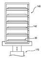
도 3은 도 1에 도시된 패드 카세트를 설명하기 위한 개략적은 구성도이다.
120 : 웨이퍼 척 130 : 패드 서포트 부재
140 : 패드 카세트 150 : 패드 이송 부재
160 : 척 스테이지 유닛 170 : 카세트 구동부
Claims (5)
- 반도체 소자들이 형성된 웨이퍼를 지지하기 위한 웨이퍼 척;
상기 웨이퍼 척의 상측에 배치되고, 상기 반도체 소자들에 접촉되어 전기적 검사 신호를 인가하기 위한 복수의 탐침을 구비하는 프로브 카드;
상기 탐침들로부터 이물질을 제거하기 위한 복수의 연마 패드를 복층 형태로 수납하는 패드 카세트;
상기 연마 패드들 중 하나가 탑재되는 패드 서포트 부재; 및
상기 패드 카세트와 상기 패드 서포트 부재 간에 상기 연마 패드들을 이송하기 위한 패드 이송 부재를 포함하고,
상기 프로브 카드는 상기 연마 패드들 중 상기 패드 서포트 부재에 탑재된 연마 패드에 의해 상기 탐침들의 이물이 제거되는 것을 특징으로 하는 것을 특징으로 하는 프로브 스테이션. - 제1항에 있어서,
상기 패드 카세트가 탑재되며, 상기 패드 이송 부재가 상기 패드 카세트에 상기 연마 패드를 반입 및 반출하기 용이하도록 상기 패드 카세트를 수직 방향으로 이동시키는 카세트 구동부를 더 포함하는 것을 특징으로 하는 프로브 스테이션. - 제1항에 있어서,
상기 웨이퍼 척과 상기 패드 서포트 부재의 아래에 배치되고, 상기 웨이퍼 척과 상기 패드 서포트 부재를 수직 및 수평 방향으로 이동시키는 척 스테이지 유닛을 더 포함하는 것을 특징으로 하는 프로브 스테이션. - 제3항에 있어서,
상기 웨이퍼에 대한 전기적 검사를 수행하기 위한 공정 공간을 제공하고, 상기 공정 공간에 상기 척 스테이지, 상기 프로브 카드, 상기 패드 카세트, 및 상기 패드 이송 부재가 배치되는 검사 챔버를 더 포함하는 것을 특징으로 하는 프로브 스테이션. - 제1항에 있어서,
상기 패드 카세트는 상기 패드 서포트 부재에 탑재되기 위해 대기중인 연마 패드들과 상기 탐침들의 이물을 제거하는데 사용된 후 외부로 반출하기 위해 대기중인 연마 패드들을 수납하는 것을 특징으로 하는 프로브 스테이션.
Priority Applications (1)
| Application Number | Priority Date | Filing Date | Title |
|---|---|---|---|
| KR1020150155757A KR102503282B1 (ko) | 2015-11-06 | 2015-11-06 | 프로브 스테이션 |
Applications Claiming Priority (1)
| Application Number | Priority Date | Filing Date | Title |
|---|---|---|---|
| KR1020150155757A KR102503282B1 (ko) | 2015-11-06 | 2015-11-06 | 프로브 스테이션 |
Publications (2)
| Publication Number | Publication Date |
|---|---|
| KR20170053775A true KR20170053775A (ko) | 2017-05-17 |
| KR102503282B1 KR102503282B1 (ko) | 2023-02-24 |
Family
ID=59048706
Family Applications (1)
| Application Number | Title | Priority Date | Filing Date |
|---|---|---|---|
| KR1020150155757A Active KR102503282B1 (ko) | 2015-11-06 | 2015-11-06 | 프로브 스테이션 |
Country Status (1)
| Country | Link |
|---|---|
| KR (1) | KR102503282B1 (ko) |
Cited By (2)
| Publication number | Priority date | Publication date | Assignee | Title |
|---|---|---|---|---|
| KR20200065660A (ko) | 2018-11-30 | 2020-06-09 | 세메스 주식회사 | 프로브 카드의 탐침 세정 방법 |
| KR20220054195A (ko) * | 2020-10-23 | 2022-05-02 | 도쿄엘렉트론가부시키가이샤 | 검사 장치 및 프로브의 연마 방법 |
Citations (4)
| Publication number | Priority date | Publication date | Assignee | Title |
|---|---|---|---|---|
| JP2007227840A (ja) * | 2006-02-27 | 2007-09-06 | Hitachi High-Tech De Technology Co Ltd | プローブ針のクリーニング装置 |
| KR20100056725A (ko) | 2008-11-20 | 2010-05-28 | 주식회사 쎄믹스 | 웨이퍼 프로브 스테이션 |
| KR20100085877A (ko) * | 2009-01-21 | 2010-07-29 | 도쿄엘렉트론가부시키가이샤 | 프로브 장치 |
| KR20150087808A (ko) | 2014-01-22 | 2015-07-30 | 도쿄엘렉트론가부시키가이샤 | 프로버 및 프로브 카드의 니들 선단 연마 장치 |
-
2015
- 2015-11-06 KR KR1020150155757A patent/KR102503282B1/ko active Active
Patent Citations (4)
| Publication number | Priority date | Publication date | Assignee | Title |
|---|---|---|---|---|
| JP2007227840A (ja) * | 2006-02-27 | 2007-09-06 | Hitachi High-Tech De Technology Co Ltd | プローブ針のクリーニング装置 |
| KR20100056725A (ko) | 2008-11-20 | 2010-05-28 | 주식회사 쎄믹스 | 웨이퍼 프로브 스테이션 |
| KR20100085877A (ko) * | 2009-01-21 | 2010-07-29 | 도쿄엘렉트론가부시키가이샤 | 프로브 장치 |
| KR20150087808A (ko) | 2014-01-22 | 2015-07-30 | 도쿄엘렉트론가부시키가이샤 | 프로버 및 프로브 카드의 니들 선단 연마 장치 |
Cited By (3)
| Publication number | Priority date | Publication date | Assignee | Title |
|---|---|---|---|---|
| KR20200065660A (ko) | 2018-11-30 | 2020-06-09 | 세메스 주식회사 | 프로브 카드의 탐침 세정 방법 |
| KR20220054195A (ko) * | 2020-10-23 | 2022-05-02 | 도쿄엘렉트론가부시키가이샤 | 검사 장치 및 프로브의 연마 방법 |
| US12259419B2 (en) | 2020-10-23 | 2025-03-25 | Tokyo Electron Limited | Test device and probe polishing method |
Also Published As
| Publication number | Publication date |
|---|---|
| KR102503282B1 (ko) | 2023-02-24 |
Similar Documents
| Publication | Publication Date | Title |
|---|---|---|
| US9671452B2 (en) | Substrate inspection apparatus and probe card transferring method | |
| KR101208773B1 (ko) | 프로브의 연마 방법 및 프로브 장치 | |
| KR101331353B1 (ko) | 프로브 카드를 세척하기 위한 방법 및 장치 | |
| US20120242359A1 (en) | Probe card detecting apparatus, wafer position alignment apparatus and wafer position alignment method | |
| KR102654604B1 (ko) | 프로브 스테이션 | |
| JPH0559841U (ja) | プロービング装置及び半導体ウエハ検査システム | |
| JP2008227148A (ja) | 半導体ウエハの試験方法およびその装置 | |
| KR20170058070A (ko) | 검사 장치용 기판 세정 모듈 및 이를 구비하는 프로브 스테이션 | |
| KR20160096021A (ko) | 박리 장치, 박리 시스템, 박리 방법 및 컴퓨터 판독 가능 정보 기억 매체 | |
| TWI880075B (zh) | 整合式cmp系統及拋光基板的方法 | |
| KR102430478B1 (ko) | 웨이퍼 검사 방법 | |
| CN102274828B (zh) | 用于测试分选机的开放装置 | |
| JP2010202392A (ja) | Icオートハンドラ | |
| KR102503282B1 (ko) | 프로브 스테이션 | |
| KR20200053587A (ko) | 검사 시스템 및 검사 방법 | |
| KR20080062673A (ko) | 웨이퍼 검사장치 및 방법 | |
| KR20170064750A (ko) | 프로브 스테이션 | |
| JPH05136219A (ja) | 検査装置 | |
| KR20170000127A (ko) | 프로브 스테이션에서 웨이퍼를 정렬하는 방법 | |
| TWI507700B (zh) | 探針台 | |
| KR102362249B1 (ko) | 프로브 스테이션 | |
| KR102699746B1 (ko) | 프로브 카드의 탐침 세정 방법 | |
| KR20150019262A (ko) | 반도체 패키지의 검사 방법 | |
| JP2006317346A (ja) | プロービングシステム及びプローバ | |
| KR102000024B1 (ko) | 검사 방법 및 기판 처리 장치 |
Legal Events
| Date | Code | Title | Description |
|---|---|---|---|
| PA0109 | Patent application |
Patent event code: PA01091R01D Comment text: Patent Application Patent event date: 20151106 |
|
| PG1501 | Laying open of application | ||
| A201 | Request for examination | ||
| PA0201 | Request for examination |
Patent event code: PA02012R01D Patent event date: 20201104 Comment text: Request for Examination of Application Patent event code: PA02011R01I Patent event date: 20151106 Comment text: Patent Application |
|
| E902 | Notification of reason for refusal | ||
| PE0902 | Notice of grounds for rejection |
Comment text: Notification of reason for refusal Patent event date: 20220719 Patent event code: PE09021S01D |
|
| E701 | Decision to grant or registration of patent right | ||
| PE0701 | Decision of registration |
Patent event code: PE07011S01D Comment text: Decision to Grant Registration Patent event date: 20230130 |
|
| GRNT | Written decision to grant | ||
| PR0701 | Registration of establishment |
Comment text: Registration of Establishment Patent event date: 20230220 Patent event code: PR07011E01D |
|
| PR1002 | Payment of registration fee |
Payment date: 20230221 End annual number: 3 Start annual number: 1 |
|
| PG1601 | Publication of registration |