KR20170053949A - 코일 부품 및 그 제조 방법 - Google Patents
코일 부품 및 그 제조 방법 Download PDFInfo
- Publication number
- KR20170053949A KR20170053949A KR1020150156523A KR20150156523A KR20170053949A KR 20170053949 A KR20170053949 A KR 20170053949A KR 1020150156523 A KR1020150156523 A KR 1020150156523A KR 20150156523 A KR20150156523 A KR 20150156523A KR 20170053949 A KR20170053949 A KR 20170053949A
- Authority
- KR
- South Korea
- Prior art keywords
- coil
- disposed
- seed layer
- layer
- pattern
- Prior art date
- Legal status (The legal status is an assumption and is not a legal conclusion. Google has not performed a legal analysis and makes no representation as to the accuracy of the status listed.)
- Granted
Links
Images





Classifications
-
- H—ELECTRICITY
- H01—ELECTRIC ELEMENTS
- H01F—MAGNETS; INDUCTANCES; TRANSFORMERS; SELECTION OF MATERIALS FOR THEIR MAGNETIC PROPERTIES
- H01F17/00—Fixed inductances of the signal type
- H01F17/0006—Printed inductances
- H01F17/0013—Printed inductances with stacked layers
-
- H—ELECTRICITY
- H01—ELECTRIC ELEMENTS
- H01F—MAGNETS; INDUCTANCES; TRANSFORMERS; SELECTION OF MATERIALS FOR THEIR MAGNETIC PROPERTIES
- H01F27/00—Details of transformers or inductances, in general
- H01F27/28—Coils; Windings; Conductive connections
- H01F27/2804—Printed windings
-
- H—ELECTRICITY
- H01—ELECTRIC ELEMENTS
- H01F—MAGNETS; INDUCTANCES; TRANSFORMERS; SELECTION OF MATERIALS FOR THEIR MAGNETIC PROPERTIES
- H01F41/00—Apparatus or processes specially adapted for manufacturing or assembling magnets, inductances or transformers; Apparatus or processes specially adapted for manufacturing materials characterised by their magnetic properties
- H01F41/02—Apparatus or processes specially adapted for manufacturing or assembling magnets, inductances or transformers; Apparatus or processes specially adapted for manufacturing materials characterised by their magnetic properties for manufacturing cores, coils, or magnets
- H01F41/04—Apparatus or processes specially adapted for manufacturing or assembling magnets, inductances or transformers; Apparatus or processes specially adapted for manufacturing materials characterised by their magnetic properties for manufacturing cores, coils, or magnets for manufacturing coils
- H01F41/041—Printed circuit coils
-
- H—ELECTRICITY
- H01—ELECTRIC ELEMENTS
- H01F—MAGNETS; INDUCTANCES; TRANSFORMERS; SELECTION OF MATERIALS FOR THEIR MAGNETIC PROPERTIES
- H01F41/00—Apparatus or processes specially adapted for manufacturing or assembling magnets, inductances or transformers; Apparatus or processes specially adapted for manufacturing materials characterised by their magnetic properties
- H01F41/02—Apparatus or processes specially adapted for manufacturing or assembling magnets, inductances or transformers; Apparatus or processes specially adapted for manufacturing materials characterised by their magnetic properties for manufacturing cores, coils, or magnets
- H01F41/04—Apparatus or processes specially adapted for manufacturing or assembling magnets, inductances or transformers; Apparatus or processes specially adapted for manufacturing materials characterised by their magnetic properties for manufacturing cores, coils, or magnets for manufacturing coils
- H01F41/041—Printed circuit coils
- H01F41/042—Printed circuit coils by thin film techniques
-
- H—ELECTRICITY
- H05—ELECTRIC TECHNIQUES NOT OTHERWISE PROVIDED FOR
- H05K—PRINTED CIRCUITS; CASINGS OR CONSTRUCTIONAL DETAILS OF ELECTRIC APPARATUS; MANUFACTURE OF ASSEMBLAGES OF ELECTRICAL COMPONENTS
- H05K1/00—Printed circuits
- H05K1/16—Printed circuits incorporating printed electric components, e.g. printed resistors, capacitors or inductors
- H05K1/165—Printed circuits incorporating printed electric components, e.g. printed resistors, capacitors or inductors incorporating printed inductors
-
- H—ELECTRICITY
- H05—ELECTRIC TECHNIQUES NOT OTHERWISE PROVIDED FOR
- H05K—PRINTED CIRCUITS; CASINGS OR CONSTRUCTIONAL DETAILS OF ELECTRIC APPARATUS; MANUFACTURE OF ASSEMBLAGES OF ELECTRICAL COMPONENTS
- H05K3/00—Apparatus or processes for manufacturing printed circuits
- H05K3/10—Apparatus or processes for manufacturing printed circuits in which conductive material is applied to the insulating support in such a manner as to form the desired conductive pattern
- H05K3/18—Apparatus or processes for manufacturing printed circuits in which conductive material is applied to the insulating support in such a manner as to form the desired conductive pattern using precipitation techniques to apply the conductive material
-
- H—ELECTRICITY
- H01—ELECTRIC ELEMENTS
- H01F—MAGNETS; INDUCTANCES; TRANSFORMERS; SELECTION OF MATERIALS FOR THEIR MAGNETIC PROPERTIES
- H01F17/00—Fixed inductances of the signal type
- H01F2017/0093—Common mode choke coil
-
- H—ELECTRICITY
- H01—ELECTRIC ELEMENTS
- H01F—MAGNETS; INDUCTANCES; TRANSFORMERS; SELECTION OF MATERIALS FOR THEIR MAGNETIC PROPERTIES
- H01F27/00—Details of transformers or inductances, in general
- H01F27/28—Coils; Windings; Conductive connections
- H01F27/2804—Printed windings
- H01F2027/2809—Printed windings on stacked layers
-
- H—ELECTRICITY
- H01—ELECTRIC ELEMENTS
- H01F—MAGNETS; INDUCTANCES; TRANSFORMERS; SELECTION OF MATERIALS FOR THEIR MAGNETIC PROPERTIES
- H01F27/00—Details of transformers or inductances, in general
- H01F27/24—Magnetic cores
- H01F27/26—Fastening parts of the core together; Fastening or mounting the core on casing or support
- H01F27/266—Fastening or mounting the core on casing or support
-
- H—ELECTRICITY
- H01—ELECTRIC ELEMENTS
- H01F—MAGNETS; INDUCTANCES; TRANSFORMERS; SELECTION OF MATERIALS FOR THEIR MAGNETIC PROPERTIES
- H01F27/00—Details of transformers or inductances, in general
- H01F27/28—Coils; Windings; Conductive connections
- H01F27/29—Terminals; Tapping arrangements for signal inductances
- H01F27/292—Surface mounted devices
Landscapes
- Engineering & Computer Science (AREA)
- Power Engineering (AREA)
- Manufacturing & Machinery (AREA)
- Microelectronics & Electronic Packaging (AREA)
- Coils Or Transformers For Communication (AREA)
- Manufacturing Cores, Coils, And Magnets (AREA)
Abstract
Description
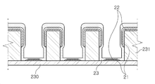
도 2는 도 1의 코일 부품의 개략적인 I-I' 면 절단 단면도이다.
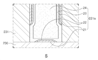
도 3은 도 2의 코일 부품의 S 영역의 개략적인 확대 단면도이다.
도 4a 내지 도 4d는 코일 부품의 개략적인 제조 공정 일례를 도시한다.
200: 코일부 210, 220: 코일 패턴
230: 기판 231: 절연층
211a, 211b, 221a, 221b: 코일 패턴
212a, 212b, 222a, 222b: 비아 연결용 패턴
232a. 232b: 비아 패턴
213a, 213b, 223a, 223b: 인출 단자
301a, 301b, 302a, 302b: 외부 전극
21, 22: 제1 시드층 23: 제2 시드층
24: 금속층
Claims (14)
- 기판과 상기 기판 상에 배치된 코일부를 포함하는 코일 부품에 있어서,
상기 코일부는 오프닝 패턴을 갖는 절연층과 그 내부에 배치된 코일 패턴을 포함하며,
상기 코일 패턴은,
상기 오프닝 패턴 내부의 측면의 일부와 하면의 일부에 배치된 제1 시드층과 상기 제1 시드층을 덮도록 배치된 제2 시드층 및 상기 제2 시드층 상에 배치된 금속층을 포함하는 코일 부품.
- 제1항에 있어서,
상기 제1 시드층은 복수의 층으로 배치된 코일 부품.
- 제2항에 있어서,
상기 제1 시드층은 티타늄(Ti), 몰리브덴(Mo), 텅스텐(W) 및 탄탈(Ta) 중의 어느 하나 이상을 포함하는 층과 그 상부에 배치되는 구리(Cu)를 포함하는 층으로 구성된 코일 부품.
- 제1항에 있어서,
상기 코일 패턴은 적어도 3층 이상의 구리를 포함하는 층으로 구성된 코일 부품.
- 제1항에 있어서,
상기 제2 시드층은 무전해 도금으로 형성된 코일 부품.
- 제1항에 있어서,
상기 제2 시드층은 상기 오프닝 패턴 내부의 측면과 하면 전부를 덮도록 배치된 코일 부품.
- 제1항에 있어서,
상기 금속층은 구리를 포함하며, 전해 도금으로 형성된 코일 부품.
- 기판과 상기 기판 상에 배치된 코일부를 포함하는 코일 부품에 있어서,
상기 코일부는 오프닝 패턴을 갖는 절연층과 그 내부에 배치된 코일 패턴을 포함하며,
상기 오프닝 패턴 내부의 측면의 일부와 하면의 일부에는 적어도 3층 이상의 구리를 포함하는 층이 배치된 코일 부품.
- 제8항에 있어서,
상기 오프닝 패턴 내부에서 적어도 3층 이상의 구리를 포함하는 층이 배치된 영역 이외의 영역에는 무전해 도금층과 그 상부에 전해 도금층이 배치된 코일 부품.
- 제9항에 있어서,
상기 무전해 도금층은 구리(Cu)를 포함하는 코일 부품.
- 제8항에 있어서,
상기 코일 패턴은,
상기 오프닝 패턴 내부의 측면의 일부와 하면의 일부에 배치된 제1 시드층과 상기 제1 시드층을 덮도록 배치된 제2 시드층 및 상기 제2 시드층 상에 배치된 금속층을 포함하는,
코일 부품.
- 제11항에 있어서,
상기 제1 시드층은 복수의 층으로 배치된 코일 부품.
- 제11항에 있어서,
상기 제1 시드층은 티타늄(Ti), 몰리브덴(Mo), 텅스텐(W) 및 탄탈(Ta) 중의 어느 하나 이상을 포함하는 층과 그 상부에 배치되는 구리(Cu)를 포함하는 층으로 구성된 코일 부품.
- 제8항에 있어서,
상기 오프닝 패턴의 하면인 상기 기판의 노출부에는 구리를 포함하는 층이 서로 다른 수로 배치된 영역이 존재하는 코일 부품.
Priority Applications (3)
| Application Number | Priority Date | Filing Date | Title |
|---|---|---|---|
| KR1020150156523A KR102130673B1 (ko) | 2015-11-09 | 2015-11-09 | 코일 부품 및 그 제조 방법 |
| US15/200,666 US20170133145A1 (en) | 2015-11-09 | 2016-07-01 | Coil component and method of manufacturing the same |
| JP2016134850A JP7099788B2 (ja) | 2015-11-09 | 2016-07-07 | コイル部品及びその製造方法 |
Applications Claiming Priority (1)
| Application Number | Priority Date | Filing Date | Title |
|---|---|---|---|
| KR1020150156523A KR102130673B1 (ko) | 2015-11-09 | 2015-11-09 | 코일 부품 및 그 제조 방법 |
Publications (2)
| Publication Number | Publication Date |
|---|---|
| KR20170053949A true KR20170053949A (ko) | 2017-05-17 |
| KR102130673B1 KR102130673B1 (ko) | 2020-07-06 |
Family
ID=58667831
Family Applications (1)
| Application Number | Title | Priority Date | Filing Date |
|---|---|---|---|
| KR1020150156523A Active KR102130673B1 (ko) | 2015-11-09 | 2015-11-09 | 코일 부품 및 그 제조 방법 |
Country Status (3)
| Country | Link |
|---|---|
| US (1) | US20170133145A1 (ko) |
| JP (1) | JP7099788B2 (ko) |
| KR (1) | KR102130673B1 (ko) |
Cited By (1)
| Publication number | Priority date | Publication date | Assignee | Title |
|---|---|---|---|---|
| KR20190008636A (ko) * | 2017-07-17 | 2019-01-25 | 삼성전기주식회사 | 코일 부품 및 그 제조방법 |
Families Citing this family (10)
| Publication number | Priority date | Publication date | Assignee | Title |
|---|---|---|---|---|
| US10897148B2 (en) | 2016-09-23 | 2021-01-19 | Apple Inc. | Wireless charging mats with multi-layer transmitter coil arrangements |
| CN109152317B (zh) * | 2018-08-17 | 2021-04-02 | 无锡蓝沛新材料科技股份有限公司 | 一种高性能屏蔽片、制备方法及其线圈模组 |
| JP7338037B2 (ja) * | 2019-08-20 | 2023-09-04 | ステムコ カンパニー リミテッド | コイル装置 |
| JP7014859B2 (ja) | 2019-08-20 | 2022-02-01 | サムソン エレクトロ-メカニックス カンパニーリミテッド. | コイル部品およびコイル部品の製造方法 |
| JP7456134B2 (ja) * | 2019-12-03 | 2024-03-27 | Tdk株式会社 | コイル部品 |
| WO2021118932A1 (en) * | 2019-12-09 | 2021-06-17 | Instant Energy Llc | Adhesive backed induction charging device |
| JP7467910B2 (ja) * | 2019-12-24 | 2024-04-16 | Tdk株式会社 | コイル部品 |
| JP2023016157A (ja) * | 2021-07-21 | 2023-02-02 | Tdk株式会社 | コイル部品 |
| CN118044341A (zh) * | 2022-06-14 | 2024-05-14 | 住友电气工业株式会社 | 印刷布线板 |
| JP2024031535A (ja) * | 2022-08-26 | 2024-03-07 | Tdk株式会社 | コイル部品 |
Citations (3)
| Publication number | Priority date | Publication date | Assignee | Title |
|---|---|---|---|---|
| JPH09270355A (ja) * | 1996-03-29 | 1997-10-14 | Tokin Corp | 電子部品及びその製造方法 |
| KR20130049207A (ko) * | 2010-10-21 | 2013-05-13 | 티디케이가부시기가이샤 | 코일 부품 및 그 제조 방법 |
| KR20140137306A (ko) * | 2013-05-22 | 2014-12-02 | 티디케이가부시기가이샤 | 코일 부품 및 그 제조방법 |
Family Cites Families (18)
| Publication number | Priority date | Publication date | Assignee | Title |
|---|---|---|---|---|
| JP3217319B2 (ja) * | 1998-12-11 | 2001-10-09 | 松下電器産業株式会社 | 半導体装置の製造方法 |
| KR100499557B1 (ko) * | 2001-06-11 | 2005-07-07 | 주식회사 하이닉스반도체 | 반도체소자의 배선 형성방법 |
| KR100689665B1 (ko) * | 2003-11-06 | 2007-03-08 | 삼성전자주식회사 | 시스템 온 칩용 인덕터의 제조 방법 |
| JP2005191408A (ja) * | 2003-12-26 | 2005-07-14 | Matsushita Electric Ind Co Ltd | コイル導電体とその製造方法およびこれを用いた電子部品 |
| KR20050115143A (ko) * | 2004-06-03 | 2005-12-07 | 매그나칩 반도체 유한회사 | 반도체 소자의 인덕터 제조방법 |
| US20090236744A1 (en) * | 2005-03-02 | 2009-09-24 | Takao Kinoshita | Semiconductor device and method of producing the same |
| JP3816091B1 (ja) * | 2005-03-02 | 2006-08-30 | シャープ株式会社 | 半導体装置及びその製造方法 |
| US7920042B2 (en) * | 2007-09-10 | 2011-04-05 | Enpirion, Inc. | Micromagnetic device and method of forming the same |
| US20090160592A1 (en) * | 2007-12-20 | 2009-06-25 | Hopper Peter J | Helical core on-chip power inductor |
| US8513771B2 (en) * | 2010-06-07 | 2013-08-20 | Infineon Technologies Ag | Semiconductor package with integrated inductor |
| JP5381956B2 (ja) * | 2010-10-21 | 2014-01-08 | Tdk株式会社 | コイル部品 |
| KR101514499B1 (ko) * | 2012-03-15 | 2015-04-22 | 삼성전기주식회사 | 공통모드필터 제조방법 및 공통모드필터 |
| US9009951B2 (en) * | 2012-04-24 | 2015-04-21 | Cyntec Co., Ltd. | Method of fabricating an electromagnetic component |
| EP2916334A1 (en) * | 2012-10-30 | 2015-09-09 | Leap Co. Ltd. | Coil element production method |
| JP6312997B2 (ja) * | 2013-07-31 | 2018-04-18 | 新光電気工業株式会社 | コイル基板及びその製造方法、インダクタ |
| US9773588B2 (en) * | 2014-05-16 | 2017-09-26 | Rohm Co., Ltd. | Chip parts |
| WO2016013649A1 (ja) * | 2014-07-25 | 2016-01-28 | 株式会社村田製作所 | 電子部品及びその製造方法 |
| KR20160144672A (ko) * | 2015-06-09 | 2016-12-19 | 주식회사 에스에프에이반도체 | 보이스 코일 제조방법 |
-
2015
- 2015-11-09 KR KR1020150156523A patent/KR102130673B1/ko active Active
-
2016
- 2016-07-01 US US15/200,666 patent/US20170133145A1/en not_active Abandoned
- 2016-07-07 JP JP2016134850A patent/JP7099788B2/ja active Active
Patent Citations (3)
| Publication number | Priority date | Publication date | Assignee | Title |
|---|---|---|---|---|
| JPH09270355A (ja) * | 1996-03-29 | 1997-10-14 | Tokin Corp | 電子部品及びその製造方法 |
| KR20130049207A (ko) * | 2010-10-21 | 2013-05-13 | 티디케이가부시기가이샤 | 코일 부품 및 그 제조 방법 |
| KR20140137306A (ko) * | 2013-05-22 | 2014-12-02 | 티디케이가부시기가이샤 | 코일 부품 및 그 제조방법 |
Cited By (1)
| Publication number | Priority date | Publication date | Assignee | Title |
|---|---|---|---|---|
| KR20190008636A (ko) * | 2017-07-17 | 2019-01-25 | 삼성전기주식회사 | 코일 부품 및 그 제조방법 |
Also Published As
| Publication number | Publication date |
|---|---|
| US20170133145A1 (en) | 2017-05-11 |
| JP7099788B2 (ja) | 2022-07-12 |
| KR102130673B1 (ko) | 2020-07-06 |
| JP2017092444A (ja) | 2017-05-25 |
Similar Documents
| Publication | Publication Date | Title |
|---|---|---|
| KR102130673B1 (ko) | 코일 부품 및 그 제조 방법 | |
| KR102145314B1 (ko) | 코일 부품 및 그 제조 방법 | |
| KR101762028B1 (ko) | 코일부품 및 그 제조방법 | |
| US7375977B2 (en) | Multilayered electronic component | |
| US11735353B2 (en) | Inductor component and method of manufacturing same | |
| CN101763933B (zh) | 电子元件及电子元件的制造方法 | |
| JP5381956B2 (ja) | コイル部品 | |
| JP5614479B2 (ja) | コイル部品の製造方法 | |
| KR102138888B1 (ko) | 코일 부품 및 그 제조 방법 | |
| JP7306219B2 (ja) | インダクタアレイ部品およびインダクタアレイ部品内蔵基板 | |
| WO2012053439A1 (ja) | コイル部品及びその製造方法 | |
| JP6766740B2 (ja) | プリント配線基板およびスイッチングレギュレータ | |
| KR20160019266A (ko) | 칩 전자부품 및 그 실장기판 | |
| JP6569916B2 (ja) | コイル電子部品 | |
| US10629365B2 (en) | Inductor array component and board for mounting the same | |
| JP2018190828A (ja) | コイル部品 | |
| KR20160136048A (ko) | 칩 전자부품 및 그 실장기판 | |
| JP6828568B2 (ja) | コイル部品 | |
| KR102618476B1 (ko) | 코일 장치 | |
| JP2016225611A (ja) | チップインダクター | |
| JP5126338B2 (ja) | トランス部品 | |
| JP7253520B2 (ja) | インダクタ部品 | |
| KR102145308B1 (ko) | 코일 부품 및 그 제조방법 | |
| JP2018170315A (ja) | コイル部品 | |
| CN100576379C (zh) | 多层布线基板形成用具有不同材质部的片材及其形成方法 |
Legal Events
| Date | Code | Title | Description |
|---|---|---|---|
| PA0109 | Patent application |
Patent event code: PA01091R01D Comment text: Patent Application Patent event date: 20151109 |
|
| PG1501 | Laying open of application | ||
| A201 | Request for examination | ||
| PA0201 | Request for examination |
Patent event code: PA02012R01D Patent event date: 20181128 Comment text: Request for Examination of Application Patent event code: PA02011R01I Patent event date: 20151109 Comment text: Patent Application |
|
| E902 | Notification of reason for refusal | ||
| PE0902 | Notice of grounds for rejection |
Comment text: Notification of reason for refusal Patent event date: 20190930 Patent event code: PE09021S01D |
|
| E701 | Decision to grant or registration of patent right | ||
| PE0701 | Decision of registration |
Patent event code: PE07011S01D Comment text: Decision to Grant Registration Patent event date: 20200421 |
|
| GRNT | Written decision to grant | ||
| PR0701 | Registration of establishment |
Comment text: Registration of Establishment Patent event date: 20200630 Patent event code: PR07011E01D |
|
| PR1002 | Payment of registration fee |
Payment date: 20200701 End annual number: 3 Start annual number: 1 |
|
| PG1601 | Publication of registration | ||
| PR1001 | Payment of annual fee |
Payment date: 20250526 Start annual number: 6 End annual number: 6 |