KR20170054360A - 반도체 장치 - Google Patents
반도체 장치 Download PDFInfo
- Publication number
- KR20170054360A KR20170054360A KR1020170057208A KR20170057208A KR20170054360A KR 20170054360 A KR20170054360 A KR 20170054360A KR 1020170057208 A KR1020170057208 A KR 1020170057208A KR 20170057208 A KR20170057208 A KR 20170057208A KR 20170054360 A KR20170054360 A KR 20170054360A
- Authority
- KR
- South Korea
- Prior art keywords
- transistor
- wiring
- signal
- potential
- gate
- Prior art date
- Legal status (The legal status is an assumption and is not a legal conclusion. Google has not performed a legal analysis and makes no representation as to the accuracy of the status listed.)
- Granted
Links
Images








Classifications
-
- H—ELECTRICITY
- H10—SEMICONDUCTOR DEVICES; ELECTRIC SOLID-STATE DEVICES NOT OTHERWISE PROVIDED FOR
- H10D—INORGANIC ELECTRIC SEMICONDUCTOR DEVICES
- H10D86/00—Integrated devices formed in or on insulating or conducting substrates, e.g. formed in silicon-on-insulator [SOI] substrates or on stainless steel or glass substrates
- H10D86/40—Integrated devices formed in or on insulating or conducting substrates, e.g. formed in silicon-on-insulator [SOI] substrates or on stainless steel or glass substrates characterised by multiple TFTs
-
- G—PHYSICS
- G09—EDUCATION; CRYPTOGRAPHY; DISPLAY; ADVERTISING; SEALS
- G09G—ARRANGEMENTS OR CIRCUITS FOR CONTROL OF INDICATING DEVICES USING STATIC MEANS TO PRESENT VARIABLE INFORMATION
- G09G3/00—Control arrangements or circuits, of interest only in connection with visual indicators other than cathode-ray tubes
- G09G3/20—Control arrangements or circuits, of interest only in connection with visual indicators other than cathode-ray tubes for presentation of an assembly of a number of characters, e.g. a page, by composing the assembly by combination of individual elements arranged in a matrix no fixed position being assigned to or needed to be assigned to the individual characters or partial characters
- G09G3/34—Control arrangements or circuits, of interest only in connection with visual indicators other than cathode-ray tubes for presentation of an assembly of a number of characters, e.g. a page, by composing the assembly by combination of individual elements arranged in a matrix no fixed position being assigned to or needed to be assigned to the individual characters or partial characters by control of light from an independent source
- G09G3/36—Control arrangements or circuits, of interest only in connection with visual indicators other than cathode-ray tubes for presentation of an assembly of a number of characters, e.g. a page, by composing the assembly by combination of individual elements arranged in a matrix no fixed position being assigned to or needed to be assigned to the individual characters or partial characters by control of light from an independent source using liquid crystals
-
- G—PHYSICS
- G09—EDUCATION; CRYPTOGRAPHY; DISPLAY; ADVERTISING; SEALS
- G09G—ARRANGEMENTS OR CIRCUITS FOR CONTROL OF INDICATING DEVICES USING STATIC MEANS TO PRESENT VARIABLE INFORMATION
- G09G3/00—Control arrangements or circuits, of interest only in connection with visual indicators other than cathode-ray tubes
- G09G3/20—Control arrangements or circuits, of interest only in connection with visual indicators other than cathode-ray tubes for presentation of an assembly of a number of characters, e.g. a page, by composing the assembly by combination of individual elements arranged in a matrix no fixed position being assigned to or needed to be assigned to the individual characters or partial characters
-
- G—PHYSICS
- G09—EDUCATION; CRYPTOGRAPHY; DISPLAY; ADVERTISING; SEALS
- G09G—ARRANGEMENTS OR CIRCUITS FOR CONTROL OF INDICATING DEVICES USING STATIC MEANS TO PRESENT VARIABLE INFORMATION
- G09G3/00—Control arrangements or circuits, of interest only in connection with visual indicators other than cathode-ray tubes
- G09G3/20—Control arrangements or circuits, of interest only in connection with visual indicators other than cathode-ray tubes for presentation of an assembly of a number of characters, e.g. a page, by composing the assembly by combination of individual elements arranged in a matrix no fixed position being assigned to or needed to be assigned to the individual characters or partial characters
- G09G3/22—Control arrangements or circuits, of interest only in connection with visual indicators other than cathode-ray tubes for presentation of an assembly of a number of characters, e.g. a page, by composing the assembly by combination of individual elements arranged in a matrix no fixed position being assigned to or needed to be assigned to the individual characters or partial characters using controlled light sources
- G09G3/30—Control arrangements or circuits, of interest only in connection with visual indicators other than cathode-ray tubes for presentation of an assembly of a number of characters, e.g. a page, by composing the assembly by combination of individual elements arranged in a matrix no fixed position being assigned to or needed to be assigned to the individual characters or partial characters using controlled light sources using electroluminescent panels
-
- G—PHYSICS
- G09—EDUCATION; CRYPTOGRAPHY; DISPLAY; ADVERTISING; SEALS
- G09G—ARRANGEMENTS OR CIRCUITS FOR CONTROL OF INDICATING DEVICES USING STATIC MEANS TO PRESENT VARIABLE INFORMATION
- G09G3/00—Control arrangements or circuits, of interest only in connection with visual indicators other than cathode-ray tubes
- G09G3/20—Control arrangements or circuits, of interest only in connection with visual indicators other than cathode-ray tubes for presentation of an assembly of a number of characters, e.g. a page, by composing the assembly by combination of individual elements arranged in a matrix no fixed position being assigned to or needed to be assigned to the individual characters or partial characters
- G09G3/34—Control arrangements or circuits, of interest only in connection with visual indicators other than cathode-ray tubes for presentation of an assembly of a number of characters, e.g. a page, by composing the assembly by combination of individual elements arranged in a matrix no fixed position being assigned to or needed to be assigned to the individual characters or partial characters by control of light from an independent source
- G09G3/36—Control arrangements or circuits, of interest only in connection with visual indicators other than cathode-ray tubes for presentation of an assembly of a number of characters, e.g. a page, by composing the assembly by combination of individual elements arranged in a matrix no fixed position being assigned to or needed to be assigned to the individual characters or partial characters by control of light from an independent source using liquid crystals
- G09G3/3611—Control of matrices with row and column drivers
- G09G3/3685—Details of drivers for data electrodes
- G09G3/3688—Details of drivers for data electrodes suitable for active matrices only
-
- G—PHYSICS
- G11—INFORMATION STORAGE
- G11C—STATIC STORES
- G11C19/00—Digital stores in which the information is moved stepwise, e.g. shift registers
- G11C19/18—Digital stores in which the information is moved stepwise, e.g. shift registers using capacitors as main elements of the stages
- G11C19/182—Digital stores in which the information is moved stepwise, e.g. shift registers using capacitors as main elements of the stages in combination with semiconductor elements, e.g. bipolar transistors, diodes
- G11C19/184—Digital stores in which the information is moved stepwise, e.g. shift registers using capacitors as main elements of the stages in combination with semiconductor elements, e.g. bipolar transistors, diodes with field-effect transistors, e.g. MOS-FET
-
- G—PHYSICS
- G11—INFORMATION STORAGE
- G11C—STATIC STORES
- G11C19/00—Digital stores in which the information is moved stepwise, e.g. shift registers
- G11C19/28—Digital stores in which the information is moved stepwise, e.g. shift registers using semiconductor elements
-
- H01L27/1214—
-
- H—ELECTRICITY
- H03—ELECTRONIC CIRCUITRY
- H03K—PULSE TECHNIQUE
- H03K17/00—Electronic switching or gating, i.e. not by contact-making and –breaking
- H03K17/06—Modifications for ensuring a fully conducting state
-
- H—ELECTRICITY
- H03—ELECTRONIC CIRCUITRY
- H03K—PULSE TECHNIQUE
- H03K17/00—Electronic switching or gating, i.e. not by contact-making and –breaking
- H03K17/08—Modifications for protecting switching circuit against overcurrent or overvoltage
- H03K17/081—Modifications for protecting switching circuit against overcurrent or overvoltage without feedback from the output circuit to the control circuit
- H03K17/08104—Modifications for protecting switching circuit against overcurrent or overvoltage without feedback from the output circuit to the control circuit in field-effect transistor switches
-
- H—ELECTRICITY
- H03—ELECTRONIC CIRCUITRY
- H03K—PULSE TECHNIQUE
- H03K19/00—Logic circuits, i.e. having at least two inputs acting on one output; Inverting circuits
- H03K19/01—Modifications for accelerating switching
- H03K19/017—Modifications for accelerating switching in field-effect transistor circuits
- H03K19/01707—Modifications for accelerating switching in field-effect transistor circuits in asynchronous circuits
- H03K19/01714—Modifications for accelerating switching in field-effect transistor circuits in asynchronous circuits by bootstrapping, i.e. by positive feed-back
-
- H—ELECTRICITY
- H03—ELECTRONIC CIRCUITRY
- H03K—PULSE TECHNIQUE
- H03K19/00—Logic circuits, i.e. having at least two inputs acting on one output; Inverting circuits
- H03K19/0175—Coupling arrangements; Interface arrangements
- H03K19/0185—Coupling arrangements; Interface arrangements using field effect transistors only
- H03K19/018507—Interface arrangements
- H03K19/018521—Interface arrangements of complementary type, e.g. CMOS
-
- H—ELECTRICITY
- H03—ELECTRONIC CIRCUITRY
- H03K—PULSE TECHNIQUE
- H03K3/00—Circuits for generating electric pulses; Monostable, bistable or multistable circuits
- H03K3/02—Generators characterised by the type of circuit or by the means used for producing pulses
- H03K3/353—Generators characterised by the type of circuit or by the means used for producing pulses by the use, as active elements, of field-effect transistors with internal or external positive feedback
- H03K3/356—Bistable circuits
-
- H—ELECTRICITY
- H10—SEMICONDUCTOR DEVICES; ELECTRIC SOLID-STATE DEVICES NOT OTHERWISE PROVIDED FOR
- H10D—INORGANIC ELECTRIC SEMICONDUCTOR DEVICES
- H10D86/00—Integrated devices formed in or on insulating or conducting substrates, e.g. formed in silicon-on-insulator [SOI] substrates or on stainless steel or glass substrates
- H10D86/01—Manufacture or treatment
- H10D86/021—Manufacture or treatment of multiple TFTs
-
- H—ELECTRICITY
- H10—SEMICONDUCTOR DEVICES; ELECTRIC SOLID-STATE DEVICES NOT OTHERWISE PROVIDED FOR
- H10D—INORGANIC ELECTRIC SEMICONDUCTOR DEVICES
- H10D86/00—Integrated devices formed in or on insulating or conducting substrates, e.g. formed in silicon-on-insulator [SOI] substrates or on stainless steel or glass substrates
- H10D86/40—Integrated devices formed in or on insulating or conducting substrates, e.g. formed in silicon-on-insulator [SOI] substrates or on stainless steel or glass substrates characterised by multiple TFTs
- H10D86/421—Integrated devices formed in or on insulating or conducting substrates, e.g. formed in silicon-on-insulator [SOI] substrates or on stainless steel or glass substrates characterised by multiple TFTs having a particular composition, shape or crystalline structure of the active layer
- H10D86/423—Integrated devices formed in or on insulating or conducting substrates, e.g. formed in silicon-on-insulator [SOI] substrates or on stainless steel or glass substrates characterised by multiple TFTs having a particular composition, shape or crystalline structure of the active layer comprising semiconductor materials not belonging to the Group IV, e.g. InGaZnO
-
- H—ELECTRICITY
- H10—SEMICONDUCTOR DEVICES; ELECTRIC SOLID-STATE DEVICES NOT OTHERWISE PROVIDED FOR
- H10D—INORGANIC ELECTRIC SEMICONDUCTOR DEVICES
- H10D86/00—Integrated devices formed in or on insulating or conducting substrates, e.g. formed in silicon-on-insulator [SOI] substrates or on stainless steel or glass substrates
- H10D86/40—Integrated devices formed in or on insulating or conducting substrates, e.g. formed in silicon-on-insulator [SOI] substrates or on stainless steel or glass substrates characterised by multiple TFTs
- H10D86/441—Interconnections, e.g. scanning lines
-
- H—ELECTRICITY
- H10—SEMICONDUCTOR DEVICES; ELECTRIC SOLID-STATE DEVICES NOT OTHERWISE PROVIDED FOR
- H10D—INORGANIC ELECTRIC SEMICONDUCTOR DEVICES
- H10D86/00—Integrated devices formed in or on insulating or conducting substrates, e.g. formed in silicon-on-insulator [SOI] substrates or on stainless steel or glass substrates
- H10D86/40—Integrated devices formed in or on insulating or conducting substrates, e.g. formed in silicon-on-insulator [SOI] substrates or on stainless steel or glass substrates characterised by multiple TFTs
- H10D86/481—Integrated devices formed in or on insulating or conducting substrates, e.g. formed in silicon-on-insulator [SOI] substrates or on stainless steel or glass substrates characterised by multiple TFTs integrated with passive devices, e.g. auxiliary capacitors
-
- H—ELECTRICITY
- H10—SEMICONDUCTOR DEVICES; ELECTRIC SOLID-STATE DEVICES NOT OTHERWISE PROVIDED FOR
- H10D—INORGANIC ELECTRIC SEMICONDUCTOR DEVICES
- H10D86/00—Integrated devices formed in or on insulating or conducting substrates, e.g. formed in silicon-on-insulator [SOI] substrates or on stainless steel or glass substrates
- H10D86/40—Integrated devices formed in or on insulating or conducting substrates, e.g. formed in silicon-on-insulator [SOI] substrates or on stainless steel or glass substrates characterised by multiple TFTs
- H10D86/60—Integrated devices formed in or on insulating or conducting substrates, e.g. formed in silicon-on-insulator [SOI] substrates or on stainless steel or glass substrates characterised by multiple TFTs wherein the TFTs are in active matrices
-
- G—PHYSICS
- G02—OPTICS
- G02F—OPTICAL DEVICES OR ARRANGEMENTS FOR THE CONTROL OF LIGHT BY MODIFICATION OF THE OPTICAL PROPERTIES OF THE MEDIA OF THE ELEMENTS INVOLVED THEREIN; NON-LINEAR OPTICS; FREQUENCY-CHANGING OF LIGHT; OPTICAL LOGIC ELEMENTS; OPTICAL ANALOGUE/DIGITAL CONVERTERS
- G02F1/00—Devices or arrangements for the control of the intensity, colour, phase, polarisation or direction of light arriving from an independent light source, e.g. switching, gating or modulating; Non-linear optics
- G02F1/01—Devices or arrangements for the control of the intensity, colour, phase, polarisation or direction of light arriving from an independent light source, e.g. switching, gating or modulating; Non-linear optics for the control of the intensity, phase, polarisation or colour
- G02F1/13—Devices or arrangements for the control of the intensity, colour, phase, polarisation or direction of light arriving from an independent light source, e.g. switching, gating or modulating; Non-linear optics for the control of the intensity, phase, polarisation or colour based on liquid crystals, e.g. single liquid crystal display cells
- G02F1/133—Constructional arrangements; Operation of liquid crystal cells; Circuit arrangements
- G02F1/136—Liquid crystal cells structurally associated with a semi-conducting layer or substrate, e.g. cells forming part of an integrated circuit
- G02F1/1362—Active matrix addressed cells
- G02F1/1368—Active matrix addressed cells in which the switching element is a three-electrode device
-
- G—PHYSICS
- G02—OPTICS
- G02F—OPTICAL DEVICES OR ARRANGEMENTS FOR THE CONTROL OF LIGHT BY MODIFICATION OF THE OPTICAL PROPERTIES OF THE MEDIA OF THE ELEMENTS INVOLVED THEREIN; NON-LINEAR OPTICS; FREQUENCY-CHANGING OF LIGHT; OPTICAL LOGIC ELEMENTS; OPTICAL ANALOGUE/DIGITAL CONVERTERS
- G02F1/00—Devices or arrangements for the control of the intensity, colour, phase, polarisation or direction of light arriving from an independent light source, e.g. switching, gating or modulating; Non-linear optics
- G02F1/01—Devices or arrangements for the control of the intensity, colour, phase, polarisation or direction of light arriving from an independent light source, e.g. switching, gating or modulating; Non-linear optics for the control of the intensity, phase, polarisation or colour
- G02F1/165—Devices or arrangements for the control of the intensity, colour, phase, polarisation or direction of light arriving from an independent light source, e.g. switching, gating or modulating; Non-linear optics for the control of the intensity, phase, polarisation or colour based on translational movement of particles in a fluid under the influence of an applied field
- G02F1/166—Devices or arrangements for the control of the intensity, colour, phase, polarisation or direction of light arriving from an independent light source, e.g. switching, gating or modulating; Non-linear optics for the control of the intensity, phase, polarisation or colour based on translational movement of particles in a fluid under the influence of an applied field characterised by the electro-optical or magneto-optical effect
- G02F1/167—Devices or arrangements for the control of the intensity, colour, phase, polarisation or direction of light arriving from an independent light source, e.g. switching, gating or modulating; Non-linear optics for the control of the intensity, phase, polarisation or colour based on translational movement of particles in a fluid under the influence of an applied field characterised by the electro-optical or magneto-optical effect by electrophoresis
-
- G—PHYSICS
- G09—EDUCATION; CRYPTOGRAPHY; DISPLAY; ADVERTISING; SEALS
- G09G—ARRANGEMENTS OR CIRCUITS FOR CONTROL OF INDICATING DEVICES USING STATIC MEANS TO PRESENT VARIABLE INFORMATION
- G09G2300/00—Aspects of the constitution of display devices
- G09G2300/04—Structural and physical details of display devices
- G09G2300/0421—Structural details of the set of electrodes
- G09G2300/0426—Layout of electrodes and connections
-
- G—PHYSICS
- G09—EDUCATION; CRYPTOGRAPHY; DISPLAY; ADVERTISING; SEALS
- G09G—ARRANGEMENTS OR CIRCUITS FOR CONTROL OF INDICATING DEVICES USING STATIC MEANS TO PRESENT VARIABLE INFORMATION
- G09G2300/00—Aspects of the constitution of display devices
- G09G2300/08—Active matrix structure, i.e. with use of active elements, inclusive of non-linear two terminal elements, in the pixels together with light emitting or modulating elements
- G09G2300/0809—Several active elements per pixel in active matrix panels
- G09G2300/0819—Several active elements per pixel in active matrix panels used for counteracting undesired variations, e.g. feedback or autozeroing
-
- G—PHYSICS
- G09—EDUCATION; CRYPTOGRAPHY; DISPLAY; ADVERTISING; SEALS
- G09G—ARRANGEMENTS OR CIRCUITS FOR CONTROL OF INDICATING DEVICES USING STATIC MEANS TO PRESENT VARIABLE INFORMATION
- G09G2300/00—Aspects of the constitution of display devices
- G09G2300/08—Active matrix structure, i.e. with use of active elements, inclusive of non-linear two terminal elements, in the pixels together with light emitting or modulating elements
- G09G2300/0876—Supplementary capacities in pixels having special driving circuits and electrodes instead of being connected to common electrode or ground; Use of additional capacitively coupled compensation electrodes
-
- G—PHYSICS
- G09—EDUCATION; CRYPTOGRAPHY; DISPLAY; ADVERTISING; SEALS
- G09G—ARRANGEMENTS OR CIRCUITS FOR CONTROL OF INDICATING DEVICES USING STATIC MEANS TO PRESENT VARIABLE INFORMATION
- G09G2310/00—Command of the display device
- G09G2310/02—Addressing, scanning or driving the display screen or processing steps related thereto
- G09G2310/0264—Details of driving circuits
- G09G2310/0286—Details of a shift registers arranged for use in a driving circuit
-
- G—PHYSICS
- G09—EDUCATION; CRYPTOGRAPHY; DISPLAY; ADVERTISING; SEALS
- G09G—ARRANGEMENTS OR CIRCUITS FOR CONTROL OF INDICATING DEVICES USING STATIC MEANS TO PRESENT VARIABLE INFORMATION
- G09G2320/00—Control of display operating conditions
- G09G2320/04—Maintaining the quality of display appearance
- G09G2320/043—Preventing or counteracting the effects of ageing
-
- G—PHYSICS
- G09—EDUCATION; CRYPTOGRAPHY; DISPLAY; ADVERTISING; SEALS
- G09G—ARRANGEMENTS OR CIRCUITS FOR CONTROL OF INDICATING DEVICES USING STATIC MEANS TO PRESENT VARIABLE INFORMATION
- G09G2330/00—Aspects of power supply; Aspects of display protection and defect management
- G09G2330/02—Details of power systems and of start or stop of display operation
- G09G2330/021—Power management, e.g. power saving
-
- G—PHYSICS
- G09—EDUCATION; CRYPTOGRAPHY; DISPLAY; ADVERTISING; SEALS
- G09G—ARRANGEMENTS OR CIRCUITS FOR CONTROL OF INDICATING DEVICES USING STATIC MEANS TO PRESENT VARIABLE INFORMATION
- G09G3/00—Control arrangements or circuits, of interest only in connection with visual indicators other than cathode-ray tubes
- G09G3/20—Control arrangements or circuits, of interest only in connection with visual indicators other than cathode-ray tubes for presentation of an assembly of a number of characters, e.g. a page, by composing the assembly by combination of individual elements arranged in a matrix no fixed position being assigned to or needed to be assigned to the individual characters or partial characters
- G09G3/22—Control arrangements or circuits, of interest only in connection with visual indicators other than cathode-ray tubes for presentation of an assembly of a number of characters, e.g. a page, by composing the assembly by combination of individual elements arranged in a matrix no fixed position being assigned to or needed to be assigned to the individual characters or partial characters using controlled light sources
- G09G3/30—Control arrangements or circuits, of interest only in connection with visual indicators other than cathode-ray tubes for presentation of an assembly of a number of characters, e.g. a page, by composing the assembly by combination of individual elements arranged in a matrix no fixed position being assigned to or needed to be assigned to the individual characters or partial characters using controlled light sources using electroluminescent panels
- G09G3/32—Control arrangements or circuits, of interest only in connection with visual indicators other than cathode-ray tubes for presentation of an assembly of a number of characters, e.g. a page, by composing the assembly by combination of individual elements arranged in a matrix no fixed position being assigned to or needed to be assigned to the individual characters or partial characters using controlled light sources using electroluminescent panels semiconductive, e.g. using light-emitting diodes [LED]
- G09G3/3208—Control arrangements or circuits, of interest only in connection with visual indicators other than cathode-ray tubes for presentation of an assembly of a number of characters, e.g. a page, by composing the assembly by combination of individual elements arranged in a matrix no fixed position being assigned to or needed to be assigned to the individual characters or partial characters using controlled light sources using electroluminescent panels semiconductive, e.g. using light-emitting diodes [LED] organic, e.g. using organic light-emitting diodes [OLED]
- G09G3/3225—Control arrangements or circuits, of interest only in connection with visual indicators other than cathode-ray tubes for presentation of an assembly of a number of characters, e.g. a page, by composing the assembly by combination of individual elements arranged in a matrix no fixed position being assigned to or needed to be assigned to the individual characters or partial characters using controlled light sources using electroluminescent panels semiconductive, e.g. using light-emitting diodes [LED] organic, e.g. using organic light-emitting diodes [OLED] using an active matrix
-
- G—PHYSICS
- G09—EDUCATION; CRYPTOGRAPHY; DISPLAY; ADVERTISING; SEALS
- G09G—ARRANGEMENTS OR CIRCUITS FOR CONTROL OF INDICATING DEVICES USING STATIC MEANS TO PRESENT VARIABLE INFORMATION
- G09G3/00—Control arrangements or circuits, of interest only in connection with visual indicators other than cathode-ray tubes
- G09G3/20—Control arrangements or circuits, of interest only in connection with visual indicators other than cathode-ray tubes for presentation of an assembly of a number of characters, e.g. a page, by composing the assembly by combination of individual elements arranged in a matrix no fixed position being assigned to or needed to be assigned to the individual characters or partial characters
- G09G3/34—Control arrangements or circuits, of interest only in connection with visual indicators other than cathode-ray tubes for presentation of an assembly of a number of characters, e.g. a page, by composing the assembly by combination of individual elements arranged in a matrix no fixed position being assigned to or needed to be assigned to the individual characters or partial characters by control of light from an independent source
- G09G3/3433—Control arrangements or circuits, of interest only in connection with visual indicators other than cathode-ray tubes for presentation of an assembly of a number of characters, e.g. a page, by composing the assembly by combination of individual elements arranged in a matrix no fixed position being assigned to or needed to be assigned to the individual characters or partial characters by control of light from an independent source using light modulating elements actuated by an electric field and being other than liquid crystal devices and electrochromic devices
- G09G3/344—Control arrangements or circuits, of interest only in connection with visual indicators other than cathode-ray tubes for presentation of an assembly of a number of characters, e.g. a page, by composing the assembly by combination of individual elements arranged in a matrix no fixed position being assigned to or needed to be assigned to the individual characters or partial characters by control of light from an independent source using light modulating elements actuated by an electric field and being other than liquid crystal devices and electrochromic devices based on particles moving in a fluid or in a gas, e.g. electrophoretic devices
-
- G—PHYSICS
- G09—EDUCATION; CRYPTOGRAPHY; DISPLAY; ADVERTISING; SEALS
- G09G—ARRANGEMENTS OR CIRCUITS FOR CONTROL OF INDICATING DEVICES USING STATIC MEANS TO PRESENT VARIABLE INFORMATION
- G09G3/00—Control arrangements or circuits, of interest only in connection with visual indicators other than cathode-ray tubes
- G09G3/20—Control arrangements or circuits, of interest only in connection with visual indicators other than cathode-ray tubes for presentation of an assembly of a number of characters, e.g. a page, by composing the assembly by combination of individual elements arranged in a matrix no fixed position being assigned to or needed to be assigned to the individual characters or partial characters
- G09G3/34—Control arrangements or circuits, of interest only in connection with visual indicators other than cathode-ray tubes for presentation of an assembly of a number of characters, e.g. a page, by composing the assembly by combination of individual elements arranged in a matrix no fixed position being assigned to or needed to be assigned to the individual characters or partial characters by control of light from an independent source
- G09G3/36—Control arrangements or circuits, of interest only in connection with visual indicators other than cathode-ray tubes for presentation of an assembly of a number of characters, e.g. a page, by composing the assembly by combination of individual elements arranged in a matrix no fixed position being assigned to or needed to be assigned to the individual characters or partial characters by control of light from an independent source using liquid crystals
- G09G3/3611—Control of matrices with row and column drivers
- G09G3/3648—Control of matrices with row and column drivers using an active matrix
-
- H—ELECTRICITY
- H10—SEMICONDUCTOR DEVICES; ELECTRIC SOLID-STATE DEVICES NOT OTHERWISE PROVIDED FOR
- H10D—INORGANIC ELECTRIC SEMICONDUCTOR DEVICES
- H10D30/00—Field-effect transistors [FET]
- H10D30/60—Insulated-gate field-effect transistors [IGFET]
- H10D30/67—Thin-film transistors [TFT]
- H10D30/674—Thin-film transistors [TFT] characterised by the active materials
- H10D30/6755—Oxide semiconductors, e.g. zinc oxide, copper aluminium oxide or cadmium stannate
-
- H—ELECTRICITY
- H10—SEMICONDUCTOR DEVICES; ELECTRIC SOLID-STATE DEVICES NOT OTHERWISE PROVIDED FOR
- H10K—ORGANIC ELECTRIC SOLID-STATE DEVICES
- H10K59/00—Integrated devices, or assemblies of multiple devices, comprising at least one organic light-emitting element covered by group H10K50/00
- H10K59/10—OLED displays
- H10K59/12—Active-matrix OLED [AMOLED] displays
Landscapes
- Engineering & Computer Science (AREA)
- Physics & Mathematics (AREA)
- Computer Hardware Design (AREA)
- General Physics & Mathematics (AREA)
- Theoretical Computer Science (AREA)
- Microelectronics & Electronic Packaging (AREA)
- Mathematical Physics (AREA)
- Chemical & Material Sciences (AREA)
- Crystallography & Structural Chemistry (AREA)
- Computing Systems (AREA)
- General Engineering & Computer Science (AREA)
- Power Engineering (AREA)
- Nonlinear Science (AREA)
- Optics & Photonics (AREA)
- Control Of Indicators Other Than Cathode Ray Tubes (AREA)
- Logic Circuits (AREA)
- Shift Register Type Memory (AREA)
- Thin Film Transistor (AREA)
- Liquid Crystal Display Device Control (AREA)
- Electronic Switches (AREA)
- Metal-Oxide And Bipolar Metal-Oxide Semiconductor Integrated Circuits (AREA)
- Control Of El Displays (AREA)
- Junction Field-Effect Transistors (AREA)
- Semiconductor Integrated Circuits (AREA)
Abstract
개시하는 발명의 일 형태의 반도체 장치는, 제 1 전위를 제 1 배선에 공급하는 기능을 갖는 제 1 트랜지스터와, 제 2 전위를 제 1 배선에 공급하는 기능을 갖는 제 2 트랜지스터와, 제 1 트랜지스터의 게이트에 제 1 트랜지스터가 온이 되기 위한 제 3 전위를 공급한 후, 제 3 전위의 공급을 멈추는 기능을 갖는 제 3 트랜지스터와, 제 2 전위를 제 1 트랜지스터의 게이트에 공급하는 기능을 갖는 제 4 트랜지스터와, 제 1 신호에 오프셋을 가한 제 2 신호를 생성하는 기능을 갖는 제 1 회로를 가지며, 제 4 트랜지스터의 게이트에는, 제 2 신호가 입력되고, 제 2 신호의 최소값은, 제 2 전위 미만의 값이다.
Description
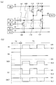
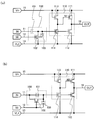
도 2는 본 발명의 일 형태에 따르는 반도체 장치를 설명하기 위한 도면.
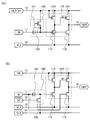
도 3은 본 발명의 일 형태에 따르는 반도체 장치를 설명하기 위한 도면.
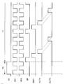
도 4는 본 발명의 일 형태에 따르는 반도체 장치를 설명하기 위한 도면.
도 5는 본 발명의 일 형태에 따르는 반도체 장치를 설명하기 위한 도면.
도 6은 본 발명의 일 형태에 따르는 반도체 장치를 설명하기 위한 도면.
도 7은 본 발명의 일 형태에 따르는 반도체 장치를 설명하기 위한 도면.
도 8은 본 발명의 일 형태에 따르는 반도체 장치를 설명하기 위한 도면.
도 9는 본 발명의 일 형태에 따르는 반도체 장치를 설명하기 위한 도면.
도 10은 본 발명의 일 형태에 따르는 반도체 장치를 설명하기 위한 도면.
도 11은 본 발명의 일 형태에 따르는 시프트 레지스터 회로를 설명하기 위한 도면.
도 12는 본 발명의 일 형태에 따르는 시프트 레지스터 회로를 설명하기 위한 도면.
도 13은 본 발명의 일 형태에 따르는 표시 장치를 설명하기 위한 도면.
도 14는 본 발명의 일 형태에 따르는 산화물 재료의 구조를 설명하는 도면.
도 15는 본 발명의 일 형태에 따르는 산화물 재료의 구조를 설명하는 도면.
도 16은 본 발명의 일 형태에 따르는 산화물 재료의 구조를 설명하는 도면.
도 17은 본 발명의 일 형태에 따르는 트랜지스터의 구조를 설명하는 도면.
도 18은 산화물 반도체층을 사용한 트랜지스터 특성의 그래프.
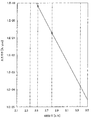
도 19는 트랜지스터의 오프 전류와 측정시 기판 온도의 관계를 도시하는 도면.
도 20은 본 발명의 일 형태에 따르는 전자 기기를 설명하는 도면.
도 21은 본 발명의 일 형태에 따르는 전자 기기를 설명하는 도면.
도 22는 본 발명의 일 형태에 따르는 반도체 장치를 설명하기 위한 도면.
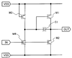
도 23은 종래의 구동 회로를 설명하는 도면.

13; 배선 14; 배선
15; 배선 16; 배선
17; 배선 21; 배선
22; 배선 23; 배선
24; 배선 25; 배선
31; 배선 31_i; 배선
31_i-1; 배선 32; 배선
33; 배선 34; 배선
35; 배선 36; 배선
37; 배선 38; 배선
100; 회로 101; 용량 소자
102; 트랜지스터 103; 용량 소자
110; 회로 111; 트랜지스터
112; 트랜지스터 113; 트랜지스터
114; 트랜지스터 115; 트랜지스터
116; 트랜지스터 120; 회로
121; 트랜지스터 122; 트랜지스터
123; 트랜지스터 124; 트랜지스터
125; 트랜지스터 126; 트랜지스터
200; 플립플롭 회로 200_1; 플립플롭 회로
200_2; 플립플롭 회로 200_3; 플립플롭 회로
600; 피소자 형성층 601; 도전층
602; 절연층 603; 산화물 반도체층
606; 절연층 608; 도전층
100A; 회로 100B; 회로
101A; 용량 소자 101B; 용량 소자
102A; 트랜지스터 102B; 트랜지스터
4001; 기판 4002; 화소부
4003; 신호선 구동 회로 4004; 주사선 구동 회로
4005; 씰재 4006; 기판
4018; FPC 4018a; FPC
4018b; FPC 604a; 영역
604b; 영역 605a; 도전층
605b; 도전층 9630; 하우징
9631; 표시부 9632; 조작 키
9633; 스피커 9635; 조작 키
9636; 접속 단자 9638; 마이크로 폰
9651; 태양 전지 9652; 배터리
9653; 윈도우형 표시부 9672; 기록 매체 판독부
9676; 셔터 버튼 9677; 수상부
9680; 외부 접속 포트 9681; 포인팅 디바이스
IN; 신호 INO; 신호
IN1; 신호 IN1O; 신호
IN2; 신호 IN2O; 신호
IN3; 신호 SE; 신호
OUT; 신호 OUTA; 신호
OUTB; 신호 OUT1; 신호
OUT2; 신호 OUTN; 신호
VH; 전위 VDD; 전위
VL1; 전위 VL2; 전위
N1; 노드 T0; 기간
T1; 기간 Ta; 기간
Tb; 기간 Tc; 기간
Td; 기간 CK; 신호
CK1; 신호 CK2; 신호
SP; 신호 M1; 트랜지스터
M2; 트랜지스터 M3; 트랜지스터
M4; 트랜지스터 C1; 용량 소자
Claims (8)
- 반도체 장치에 있어서,
제 1 트랜지스터;
제 2 트랜지스터;
제 3 트랜지스터;
제 4 트랜지스터;
제 5 트랜지스터; 및
용량 소자를 포함하고,
상기 제 1 트랜지스터의 소스 및 드레인 중 하나는 상기 제 2 트랜지스터의 소스 및 드레인 중 하나와 전기적으로 접속되고,
상기 제 3 트랜지스터의 소스 및 드레인 중 하나는 상기 제 4 트랜지스터의 소스 및 드레인 중 하나와 전기적으로 접속되고,
상기 제 1 트랜지스터의 게이트는 상기 제 3 트랜지스터의 상기 소스 및 상기 드레인 중 상기 하나와 전기적으로 접속되고,
상기 제 2 트랜지스터의 게이트는 상기 제 4 트랜지스터의 게이트와 전기적으로 접속되고,
상기 제 3 트랜지스터의 게이트는 상기 제 3 트랜지스터의 상기 소스 및 상기 드레인 중 다른 하나와 전기적으로 접속되고,
상기 제 5 트랜지스터의 소스 및 드레인 중 하나는 상기 제 2 트랜지스터의 상기 게이트와 전기적으로 접속되고,
상기 용량 소자의 제 1 단자는 상기 제 2 트랜지스터의 상기 게이트와 전기적으로 접속되고,
상기 용량 소자의 제 2 단자는 제 1 배선과 전기적으로 접속되고,
상기 제 5 트랜지스터의 게이트는 제 2 배선과 전기적으로 접속되고,
제 1 신호가 상기 제 1 배선에 입력되고,
제 2 신호가 상기 제 2 배선에 입력되고,
상기 제 5 트랜지스터의 상기 소스 및 상기 드레인 중 다른 하나 및 상기 제 2 트랜지스터의 상기 소스 및 상기 드레인 중 다른 하나는 각각 다른 배선들과 직접 접속되는, 반도체 장치. - 제 1 항에 있어서,
상기 제 1 트랜지스터의 상기 소스 및 상기 드레인 중 상기 하나는 제 3 배선과 전기적으로 접속되고,
제 3 신호가 상기 제 3 배선으로 출력되는, 반도체 장치. - 반도체 장치에 있어서,
제 1 트랜지스터;
제 2 트랜지스터;
제 3 트랜지스터;
제 4 트랜지스터;
제 5 트랜지스터; 및
용량 소자를 포함하고,
상기 제 1 트랜지스터의 소스 및 드레인 중 하나는 상기 제 2 트랜지스터의 소스 및 드레인 중 하나와 전기적으로 접속되고,
상기 제 3 트랜지스터의 소스 및 드레인 중 하나는 상기 제 4 트랜지스터의 소스 및 드레인 중 하나와 전기적으로 접속되고,
상기 제 1 트랜지스터의 게이트는 상기 제 3 트랜지스터의 상기 소스 및 상기 드레인 중 상기 하나와 전기적으로 접속되고,
상기 제 2 트랜지스터의 게이트는 상기 제 4 트랜지스터의 게이트와 전기적으로 접속되고,
상기 제 3 트랜지스터의 게이트는 상기 제 3 트랜지스터의 상기 소스 및 상기 드레인 중 다른 하나와 전기적으로 접속되고,
상기 제 5 트랜지스터의 소스 및 드레인 중 하나는 상기 제 2 트랜지스터의 상기 게이트와 전기적으로 접속되고,
상기 용량 소자의 제 1 단자는 상기 제 2 트랜지스터의 상기 게이트와 전기적으로 접속되고,
제 1 신호가 상기 용량 소자의 제 2 단자에 입력되고,
제 2 신호가 상기 제 5 트랜지스터의 게이트에 입력되고,
상기 제 5 트랜지스터의 상기 소스 및 상기 드레인 중 다른 하나 및 상기 제 2 트랜지스터의 상기 소스 및 상기 드레인 중 다른 하나는 각각 다른 배선들과 직접 접속되는, 반도체 장치. - 제 3 항에 있어서,
제 3 신호가 상기 제 1 트랜지스터의 상기 소스 및 상기 드레인 중 상기 하나로부터 출력되는, 반도체 장치. - 반도체 장치에 있어서,
제 1 트랜지스터;
제 2 트랜지스터;
제 3 트랜지스터;
제 4 트랜지스터;
제 5 트랜지스터; 및
용량 소자를 포함하고,
상기 반도체 장치는 제 1 신호 및 제 2 신호에 따라 제 3 신호를 출력하고,
상기 제 1 트랜지스터의 소스 및 드레인 중 하나는 상기 제 2 트랜지스터의 소스 및 드레인 중 하나와 전기적으로 접속되고,
상기 제 3 트랜지스터의 소스 및 드레인 중 하나는 상기 제 4 트랜지스터의 소스 및 드레인 중 하나와 전기적으로 접속되고,
상기 제 1 트랜지스터의 게이트는 상기 제 3 트랜지스터의 상기 소스 및 상기 드레인 중 상기 하나와 전기적으로 접속되고,
상기 제 2 트랜지스터의 게이트는 상기 제 4 트랜지스터의 게이트와 전기적으로 접속되고,
상기 제 3 트랜지스터의 게이트는 상기 제 3 트랜지스터의 상기 소스 및 상기 드레인 중 다른 하나와 전기적으로 접속되고,
상기 제 5 트랜지스터의 소스 및 드레인 중 하나는 상기 제 2 트랜지스터의 상기 게이트와 전기적으로 접속되고,
상기 용량 소자의 제 1 단자는 상기 제 2 트랜지스터의 상기 게이트와 전기적으로 접속되고,
상기 용량 소자의 제 2 단자의 전위는 상기 제 1 신호에 기초하고,
상기 제 5 트랜지스터의 게이트의 전위는 상기 제 2 신호에 기초하고,
상기 제 1 트랜지스터의 상기 소스 및 상기 드레인 중 상기 하나의 전위는 상기 제 3 신호에 기초하고,
상기 제 5 트랜지스터의 상기 소스 및 상기 드레인 중 다른 하나 및 상기 제 2 트랜지스터의 상기 소스 및 상기 드레인 중 다른 하나는 각각 다른 배선들과 직접 접속되는, 반도체 장치. - 반도체 장치에 있어서,
제 1 트랜지스터;
제 2 트랜지스터;
제 3 트랜지스터;
제 4 트랜지스터;
제 5 트랜지스터; 및
용량 소자를 포함하고,
상기 제 1 트랜지스터의 소스 및 드레인 중 하나는 상기 제 2 트랜지스터의 소스 및 드레인 중 하나와 전기적으로 접속되고,
상기 제 3 트랜지스터의 소스 및 드레인 중 하나는 상기 제 4 트랜지스터의 소스 및 드레인 중 하나와 전기적으로 접속되고,
상기 제 1 트랜지스터의 게이트는 상기 제 3 트랜지스터의 상기 소스 및 상기 드레인 중 상기 하나와 전기적으로 접속되고,
상기 제 2 트랜지스터의 게이트는 상기 제 4 트랜지스터의 게이트와 전기적으로 접속되고,
상기 제 3 트랜지스터의 게이트는 상기 제 3 트랜지스터의 상기 소스 및 상기 드레인 중 다른 하나와 전기적으로 접속되고,
상기 제 5 트랜지스터의 소스 및 드레인 중 하나는 상기 제 2 트랜지스터의 상기 게이트와 전기적으로 접속되고,
상기 용량 소자의 제 1 단자는 상기 제 2 트랜지스터의 상기 게이트와 전기적으로 접속되고,
상기 용량 소자의 제 2 단자는 제 1 입력 단자와 전기적으로 접속되고,
상기 제 5 트랜지스터의 게이트는 제 2 입력 단자와 전기적으로 접속되고,
상기 제 1 트랜지스터의 상기 소스 및 상기 드레인 중 상기 하나는 출력 단자와 전기적으로 접속되고,
상기 제 5 트랜지스터의 상기 소스 및 상기 드레인 중 다른 하나 및 상기 제 2 트랜지스터의 상기 소스 및 상기 드레인 중 다른 하나는 각각 다른 배선들과 직접 접속되는, 반도체 장치. - 표시 모듈에 있어서,
제 1 항 내지 제 6 항 중 어느 한 항에 따른 상기 반도체 장치, 및
FPC를 포함하는, 표시 모듈. - 전자 기기에 있어서,
제 7 항에 따른 상기 표시 모듈, 및
배터리, 수상부, 외부 접속 포트, 스피커 및 조작 키 중 적어도 하나를 포함하는, 전자 기기.
Applications Claiming Priority (2)
| Application Number | Priority Date | Filing Date | Title |
|---|---|---|---|
| JP2011108133 | 2011-05-13 | ||
| JPJP-P-2011-108133 | 2011-05-13 |
Related Parent Applications (1)
| Application Number | Title | Priority Date | Filing Date |
|---|---|---|---|
| KR1020120049579A Division KR101983976B1 (ko) | 2011-05-13 | 2012-05-10 | 반도체 장치 |
Publications (2)
| Publication Number | Publication Date |
|---|---|
| KR20170054360A true KR20170054360A (ko) | 2017-05-17 |
| KR101852752B1 KR101852752B1 (ko) | 2018-04-30 |
Family
ID=47141492
Family Applications (10)
| Application Number | Title | Priority Date | Filing Date |
|---|---|---|---|
| KR1020120049579A Active KR101983976B1 (ko) | 2011-05-13 | 2012-05-10 | 반도체 장치 |
| KR1020150102743A Active KR101720509B1 (ko) | 2011-05-13 | 2015-07-21 | 반도체 장치 및 표시 장치 |
| KR1020170057208A Active KR101852752B1 (ko) | 2011-05-13 | 2017-05-08 | 반도체 장치 |
| KR1020190060364A Active KR102151397B1 (ko) | 2011-05-13 | 2019-05-23 | 반도체 장치 |
| KR1020200107889A Active KR102221936B1 (ko) | 2011-05-13 | 2020-08-26 | 반도체 장치 |
| KR1020210023519A Active KR102392242B1 (ko) | 2011-05-13 | 2021-02-22 | 반도체 장치 |
| KR1020220050237A Active KR102499477B1 (ko) | 2011-05-13 | 2022-04-22 | 반도체 장치 |
| KR1020230016626A Abandoned KR20230025421A (ko) | 2011-05-13 | 2023-02-08 | 반도체 장치 |
| KR1020240148591A Ceased KR20240158211A (ko) | 2011-05-13 | 2024-10-28 | 반도체 장치 |
| KR1020250149606A Pending KR20250153173A (ko) | 2011-05-13 | 2025-10-16 | 반도체 장치 |
Family Applications Before (2)
| Application Number | Title | Priority Date | Filing Date |
|---|---|---|---|
| KR1020120049579A Active KR101983976B1 (ko) | 2011-05-13 | 2012-05-10 | 반도체 장치 |
| KR1020150102743A Active KR101720509B1 (ko) | 2011-05-13 | 2015-07-21 | 반도체 장치 및 표시 장치 |
Family Applications After (7)
| Application Number | Title | Priority Date | Filing Date |
|---|---|---|---|
| KR1020190060364A Active KR102151397B1 (ko) | 2011-05-13 | 2019-05-23 | 반도체 장치 |
| KR1020200107889A Active KR102221936B1 (ko) | 2011-05-13 | 2020-08-26 | 반도체 장치 |
| KR1020210023519A Active KR102392242B1 (ko) | 2011-05-13 | 2021-02-22 | 반도체 장치 |
| KR1020220050237A Active KR102499477B1 (ko) | 2011-05-13 | 2022-04-22 | 반도체 장치 |
| KR1020230016626A Abandoned KR20230025421A (ko) | 2011-05-13 | 2023-02-08 | 반도체 장치 |
| KR1020240148591A Ceased KR20240158211A (ko) | 2011-05-13 | 2024-10-28 | 반도체 장치 |
| KR1020250149606A Pending KR20250153173A (ko) | 2011-05-13 | 2025-10-16 | 반도체 장치 |
Country Status (4)
| Country | Link |
|---|---|
| US (9) | US8698551B2 (ko) |
| JP (12) | JP5873755B2 (ko) |
| KR (10) | KR101983976B1 (ko) |
| TW (9) | TWI633556B (ko) |
Families Citing this family (28)
| Publication number | Priority date | Publication date | Assignee | Title |
|---|---|---|---|---|
| TWI633556B (zh) * | 2011-05-13 | 2018-08-21 | Semiconductor Energy Laboratory Co., Ltd. | 半導體裝置 |
| US9742378B2 (en) | 2012-06-29 | 2017-08-22 | Semiconductor Energy Laboratory Co., Ltd. | Pulse output circuit and semiconductor device |
| US9070546B2 (en) | 2012-09-07 | 2015-06-30 | Semiconductor Energy Laboratory Co., Ltd. | Semiconductor device |
| JP2014137398A (ja) * | 2013-01-15 | 2014-07-28 | Sony Corp | 表示装置、表示駆動装置、駆動方法、および電子機器 |
| JP6068748B2 (ja) * | 2013-03-13 | 2017-01-25 | 株式会社半導体エネルギー研究所 | 半導体装置 |
| JP6475424B2 (ja) | 2013-06-05 | 2019-02-27 | 株式会社半導体エネルギー研究所 | 半導体装置 |
| KR102072214B1 (ko) * | 2013-07-09 | 2020-02-03 | 삼성디스플레이 주식회사 | 주사 구동 장치 및 이를 포함하는 표시 장치 |
| JP6097653B2 (ja) * | 2013-08-05 | 2017-03-15 | 株式会社ジャパンディスプレイ | 薄膜トランジスタ回路およびそれを用いた表示装置 |
| KR20220046701A (ko) * | 2013-12-27 | 2022-04-14 | 가부시키가이샤 한도오따이 에네루기 켄큐쇼 | 발광 장치 |
| CN111524967B (zh) * | 2014-02-21 | 2024-07-12 | 株式会社半导体能源研究所 | 半导体膜、晶体管、半导体装置、显示装置以及电子设备 |
| TWI654613B (zh) | 2014-02-21 | 2019-03-21 | 日商半導體能源研究所股份有限公司 | 半導體裝置及電子裝置 |
| US10199006B2 (en) | 2014-04-24 | 2019-02-05 | Semiconductor Energy Laboratory Co., Ltd. | Semiconductor device, display module, and electronic device |
| JP6521794B2 (ja) | 2014-09-03 | 2019-05-29 | 株式会社半導体エネルギー研究所 | 半導体装置、及び電子機器 |
| US10068927B2 (en) * | 2014-10-23 | 2018-09-04 | Semiconductor Energy Laboratory Co., Ltd. | Semiconductor device, display module, and electronic device |
| CN104835475B (zh) * | 2015-06-08 | 2017-03-29 | 京东方科技集团股份有限公司 | 移位寄存器单元及其驱动方法、栅极驱动电路和显示装置 |
| KR20170008375A (ko) * | 2015-07-13 | 2017-01-24 | 에스케이하이닉스 주식회사 | 반도체 장치 |
| KR102473306B1 (ko) * | 2015-11-18 | 2022-12-05 | 삼성디스플레이 주식회사 | 표시 장치 |
| CN105321491B (zh) * | 2015-11-18 | 2017-11-17 | 武汉华星光电技术有限公司 | 栅极驱动电路和使用栅极驱动电路的液晶显示器 |
| WO2018003931A1 (ja) * | 2016-07-01 | 2018-01-04 | シャープ株式会社 | Tft回路およびシフトレジスタ回路 |
| CN106205539A (zh) * | 2016-08-31 | 2016-12-07 | 深圳市华星光电技术有限公司 | 一种双向扫描的栅极驱动电路、液晶显示面板 |
| TWI606438B (zh) * | 2017-02-16 | 2017-11-21 | 友達光電股份有限公司 | 移位暫存電路 |
| WO2018163985A1 (ja) * | 2017-03-10 | 2018-09-13 | シャープ株式会社 | 走査線駆動回路およびこれを備えた表示装置 |
| CN107785403B (zh) * | 2017-10-30 | 2020-04-21 | 武汉天马微电子有限公司 | 一种显示面板及显示装置 |
| TWI670703B (zh) * | 2018-06-15 | 2019-09-01 | 元太科技工業股份有限公司 | 畫素電路 |
| CN109192140B (zh) | 2018-09-27 | 2020-11-24 | 武汉华星光电半导体显示技术有限公司 | 像素驱动电路和显示装置 |
| CN111445863B (zh) * | 2020-05-14 | 2021-09-14 | 京东方科技集团股份有限公司 | 一种像素驱动电路及其驱动方法、显示装置 |
| KR102888510B1 (ko) * | 2020-12-24 | 2025-11-20 | 엘지디스플레이 주식회사 | 레벨 쉬프터 및 표시 장치 |
| KR102625976B1 (ko) * | 2022-05-27 | 2024-01-16 | 숭실대학교 산학협력단 | 안정적으로 다중 주파수에서의 동작이 가능한 게이트 드라이버 |
Family Cites Families (76)
| Publication number | Priority date | Publication date | Assignee | Title |
|---|---|---|---|---|
| DE2851111C2 (de) * | 1978-11-25 | 1980-09-25 | Deutsche Itt Industries Gmbh, 7800 Freiburg | Zweidimensionale Analog-Speicheranordnung |
| JPS6276878A (ja) * | 1985-09-30 | 1987-04-08 | Toshiba Corp | 映像スクランブル信号処理装置 |
| US5412346A (en) * | 1993-12-13 | 1995-05-02 | At&T Corp. | Variable gain voltage signal amplifier |
| US5701136A (en) * | 1995-03-06 | 1997-12-23 | Thomson Consumer Electronics S.A. | Liquid crystal display driver with threshold voltage drift compensation |
| FR2743662B1 (fr) * | 1996-01-11 | 1998-02-13 | Thomson Lcd | Perfectionnement aux registres a decalage utilisant des transistors mis de meme polarite |
| US5859630A (en) * | 1996-12-09 | 1999-01-12 | Thomson Multimedia S.A. | Bi-directional shift register |
| TW344131B (en) * | 1997-06-03 | 1998-11-01 | Nat Science Council | A 1.5V bootstrapped all-N-logic true-single-phase CMOS dynamic logic circuit suitable for low supply voltage and high speed pipelined |
| JP3017133B2 (ja) | 1997-06-26 | 2000-03-06 | 日本電気アイシーマイコンシステム株式会社 | レベルシフタ回路 |
| US6798452B1 (en) * | 1997-07-28 | 2004-09-28 | Matsushita Electric Industrial Co., Ltd. | Amplifying solid-state imaging device, method for driving the same and physical quantity distribution sensing semiconductor device |
| EP1041641B1 (en) | 1999-03-26 | 2015-11-04 | Semiconductor Energy Laboratory Co., Ltd. | A method for manufacturing an electrooptical device |
| FR2820212A1 (fr) * | 2001-01-30 | 2002-08-02 | St Microelectronics Sa | Circuit de detection de mauvaise connexion d'alimentation |
| JP4785271B2 (ja) | 2001-04-27 | 2011-10-05 | 株式会社半導体エネルギー研究所 | 液晶表示装置、電子機器 |
| JP4439761B2 (ja) * | 2001-05-11 | 2010-03-24 | 株式会社半導体エネルギー研究所 | 液晶表示装置、電子機器 |
| US6366124B1 (en) * | 2001-05-16 | 2002-04-02 | Pericom Semiconductor Corp. | BiDirectional active voltage translator with bootstrap switches for mixed-supply VLSI |
| JP4310939B2 (ja) * | 2001-06-29 | 2009-08-12 | カシオ計算機株式会社 | シフトレジスタ及び電子装置 |
| TW554558B (en) | 2001-07-16 | 2003-09-21 | Semiconductor Energy Lab | Light emitting device |
| KR100403631B1 (ko) | 2001-07-20 | 2003-10-30 | 삼성전자주식회사 | 비트라인 센스앰프 드라이버의 배치방법 |
| JP4302535B2 (ja) | 2002-04-08 | 2009-07-29 | サムスン エレクトロニクス カンパニー リミテッド | ゲート駆動回路及びこれを有する液晶表示装置 |
| TWI293444B (en) * | 2002-04-08 | 2008-02-11 | Samsung Electronics Co Ltd | Liquid crystal display device |
| JP4344698B2 (ja) | 2002-12-25 | 2009-10-14 | 株式会社半導体エネルギー研究所 | 補正回路を備えたデジタル回路及びそれを有する電子機器 |
| KR100506005B1 (ko) | 2002-12-31 | 2005-08-04 | 엘지.필립스 엘시디 주식회사 | 평판표시장치 |
| JP4401801B2 (ja) * | 2003-02-12 | 2010-01-20 | 株式会社半導体エネルギー研究所 | 半導体装置及び表示装置 |
| US7528643B2 (en) | 2003-02-12 | 2009-05-05 | Semiconductor Energy Laboratory Co., Ltd. | Semiconductor device, electronic device having the same, and driving method of the same |
| TWI228696B (en) | 2003-03-21 | 2005-03-01 | Ind Tech Res Inst | Pixel circuit for active matrix OLED and driving method |
| US7329968B2 (en) * | 2003-05-08 | 2008-02-12 | The Trustees Of Columbia University In The City Of New York | Charge-recycling voltage domains for energy-efficient low-voltage operation of digital CMOS circuits |
| GB0313041D0 (en) * | 2003-06-06 | 2003-07-09 | Koninkl Philips Electronics Nv | Display device having current-driven pixels |
| JP2005005620A (ja) | 2003-06-13 | 2005-01-06 | Toyota Industries Corp | スイッチトキャパシタ回路及びその半導体集積回路 |
| JP4565815B2 (ja) | 2003-06-27 | 2010-10-20 | 三洋電機株式会社 | 表示装置 |
| US7368896B2 (en) * | 2004-03-29 | 2008-05-06 | Ricoh Company, Ltd. | Voltage regulator with plural error amplifiers |
| KR101023726B1 (ko) * | 2004-03-31 | 2011-03-25 | 엘지디스플레이 주식회사 | 쉬프트 레지스터 |
| US7564291B2 (en) * | 2004-04-26 | 2009-07-21 | Polymer Vision Limited | Threshold voltage adjustment in thin film transistors |
| KR101057891B1 (ko) * | 2004-05-31 | 2011-08-19 | 엘지디스플레이 주식회사 | 쉬프트 레지스터 |
| KR20050121357A (ko) | 2004-06-22 | 2005-12-27 | 삼성전자주식회사 | 쉬프트 레지스터와, 이를 갖는 스캔 구동 회로 및 표시 장치 |
| GB0417132D0 (en) | 2004-07-31 | 2004-09-01 | Koninkl Philips Electronics Nv | A shift register circuit |
| JP2006178165A (ja) | 2004-12-22 | 2006-07-06 | Alps Electric Co Ltd | ドライバ回路、シフトレジスタ及び液晶駆動回路 |
| KR101110133B1 (ko) | 2004-12-28 | 2012-02-20 | 엘지디스플레이 주식회사 | 액정표시장치 게이트 구동용 쉬프트레지스터 |
| JP4993544B2 (ja) | 2005-03-30 | 2012-08-08 | 三菱電機株式会社 | シフトレジスタ回路 |
| JP4866623B2 (ja) | 2005-06-03 | 2012-02-01 | 株式会社 日立ディスプレイズ | 表示装置及びその制御方法 |
| JP2007011139A (ja) | 2005-07-01 | 2007-01-18 | Toshiba Corp | 液晶表示装置及びその製造方法 |
| JP5064747B2 (ja) | 2005-09-29 | 2012-10-31 | 株式会社半導体エネルギー研究所 | 半導体装置、電気泳動表示装置、表示モジュール、電子機器、及び半導体装置の作製方法 |
| EP1998373A3 (en) | 2005-09-29 | 2012-10-31 | Semiconductor Energy Laboratory Co, Ltd. | Semiconductor device having oxide semiconductor layer and manufacturing method thereof |
| TW200735027A (en) | 2006-01-05 | 2007-09-16 | Mitsubishi Electric Corp | Shift register and image display apparatus containing the same |
| KR101437086B1 (ko) | 2006-01-07 | 2014-09-03 | 가부시키가이샤 한도오따이 에네루기 켄큐쇼 | 반도체장치와, 이 반도체장치를 구비한 표시장치 및 전자기기 |
| JP5164383B2 (ja) * | 2006-01-07 | 2013-03-21 | 株式会社半導体エネルギー研究所 | 半導体装置、表示装置、液晶表示装置、表示モジュール及び電子機器 |
| JP4912121B2 (ja) | 2006-02-23 | 2012-04-11 | 三菱電機株式会社 | シフトレジスタ回路 |
| US7443202B2 (en) * | 2006-06-02 | 2008-10-28 | Semiconductor Energy Laboratory Co., Ltd. | Semiconductor device and electronic apparatus having the same |
| JP5069950B2 (ja) * | 2006-06-02 | 2012-11-07 | 株式会社半導体エネルギー研究所 | 半導体装置、表示装置、液晶表示装置、表示モジュール及び電子機器 |
| EP1895545B1 (en) * | 2006-08-31 | 2014-04-23 | Semiconductor Energy Laboratory Co., Ltd. | Liquid crystal display device |
| TWI347577B (en) | 2006-09-01 | 2011-08-21 | Au Optronics Corp | Shift register with low stress |
| JP5116277B2 (ja) | 2006-09-29 | 2013-01-09 | 株式会社半導体エネルギー研究所 | 半導体装置、表示装置、液晶表示装置、表示モジュール及び電子機器 |
| JP4932415B2 (ja) * | 2006-09-29 | 2012-05-16 | 株式会社半導体エネルギー研究所 | 半導体装置 |
| JP5090008B2 (ja) | 2007-02-07 | 2012-12-05 | 三菱電機株式会社 | 半導体装置およびシフトレジスタ回路 |
| JP4912186B2 (ja) | 2007-03-05 | 2012-04-11 | 三菱電機株式会社 | シフトレジスタ回路およびそれを備える画像表示装置 |
| JP2008251094A (ja) | 2007-03-30 | 2008-10-16 | Mitsubishi Electric Corp | シフトレジスタ回路およびそれを備える画像表示装置 |
| TWI337735B (en) | 2007-05-18 | 2011-02-21 | Au Optronics Corp | Liquid crystal display and shift register with individual driving node |
| JP2009017076A (ja) * | 2007-07-03 | 2009-01-22 | Seiko Epson Corp | バッファ回路及び表示装置 |
| US20100188385A1 (en) | 2007-07-24 | 2010-07-29 | Koninklijke Philips Electronics N.V. | Shift register circuit having threshold voltage compensation |
| WO2009034750A1 (ja) | 2007-09-12 | 2009-03-19 | Sharp Kabushiki Kaisha | シフトレジスタ |
| JP2009094927A (ja) * | 2007-10-11 | 2009-04-30 | Seiko Epson Corp | バッファ、レベルシフト回路及び表示装置 |
| JP5106186B2 (ja) | 2008-03-13 | 2012-12-26 | 三菱電機株式会社 | ドライバ回路 |
| US8314765B2 (en) | 2008-06-17 | 2012-11-20 | Semiconductor Energy Laboratory Co., Ltd. | Driver circuit, display device, and electronic device |
| JP5245678B2 (ja) * | 2008-09-24 | 2013-07-24 | カシオ計算機株式会社 | 信号シフト装置、シフトレジスタ、電子機器及び信号シフト装置の駆動方法 |
| KR101520807B1 (ko) * | 2009-01-05 | 2015-05-18 | 삼성디스플레이 주식회사 | 게이트 구동회로 및 이를 갖는 표시장치 |
| KR101022092B1 (ko) * | 2009-01-12 | 2011-03-17 | 삼성모바일디스플레이주식회사 | 쉬프트 레지스터 및 이를 이용한 유기전계발광 표시장치 |
| JP5484109B2 (ja) | 2009-02-09 | 2014-05-07 | 三菱電機株式会社 | 電気光学装置 |
| US8872751B2 (en) * | 2009-03-26 | 2014-10-28 | Semiconductor Energy Laboratory Co., Ltd. | Liquid crystal display device having interconnected transistors and electronic device including the same |
| KR101573460B1 (ko) * | 2009-04-30 | 2015-12-02 | 삼성디스플레이 주식회사 | 게이트 구동회로 |
| JP5436049B2 (ja) * | 2009-05-29 | 2014-03-05 | 三菱電機株式会社 | シフトレジスタ回路、シフトレジスタ回路の設計方法及び半導体装置 |
| TWI671724B (zh) | 2009-09-10 | 2019-09-11 | 日商半導體能源研究所股份有限公司 | 半導體裝置和顯示裝置 |
| CN102024410B (zh) | 2009-09-16 | 2014-10-22 | 株式会社半导体能源研究所 | 半导体装置及电子设备 |
| CN107195328B (zh) | 2009-10-09 | 2020-11-10 | 株式会社半导体能源研究所 | 移位寄存器和显示装置以及其驱动方法 |
| WO2011043451A1 (en) | 2009-10-09 | 2011-04-14 | Semiconductor Energy Laboratory Co., Ltd. | Shift register and display device |
| TWI465039B (zh) | 2009-10-15 | 2014-12-11 | Au Optronics Corp | 移位暫存器電路 |
| TWI633556B (zh) * | 2011-05-13 | 2018-08-21 | Semiconductor Energy Laboratory Co., Ltd. | 半導體裝置 |
| CN103345941B (zh) * | 2013-07-03 | 2016-12-28 | 京东方科技集团股份有限公司 | 移位寄存器单元及驱动方法、移位寄存器电路及显示装置 |
| TWI654613B (zh) * | 2014-02-21 | 2019-03-21 | 日商半導體能源研究所股份有限公司 | 半導體裝置及電子裝置 |
-
2012
- 2012-05-10 TW TW106116890A patent/TWI633556B/zh active
- 2012-05-10 KR KR1020120049579A patent/KR101983976B1/ko active Active
- 2012-05-10 TW TW113122835A patent/TW202514630A/zh unknown
- 2012-05-10 TW TW101116657A patent/TWI587306B/zh active
- 2012-05-10 TW TW110100935A patent/TW202141508A/zh unknown
- 2012-05-10 TW TW105128053A patent/TWI595495B/zh active
- 2012-05-10 JP JP2012108073A patent/JP5873755B2/ja active Active
- 2012-05-10 TW TW104123251A patent/TWI562156B/zh active
- 2012-05-10 TW TW107118004A patent/TWI673718B/zh active
- 2012-05-10 TW TW111107647A patent/TW202242890A/zh unknown
- 2012-05-10 TW TW108125620A patent/TWI717788B/zh active
- 2012-05-10 US US13/468,135 patent/US8698551B2/en active Active
-
2014
- 2014-04-11 US US14/250,623 patent/US9106224B2/en active Active
- 2014-05-20 JP JP2014104064A patent/JP5745726B2/ja active Active
-
2015
- 2015-07-02 US US14/790,309 patent/US9508301B2/en active Active
- 2015-07-21 KR KR1020150102743A patent/KR101720509B1/ko active Active
-
2016
- 2016-01-18 JP JP2016006930A patent/JP2016129338A/ja not_active Withdrawn
- 2016-11-14 US US15/350,712 patent/US10062717B2/en active Active
-
2017
- 2017-05-08 KR KR1020170057208A patent/KR101852752B1/ko active Active
- 2017-12-13 JP JP2017238199A patent/JP6564836B2/ja active Active
-
2018
- 2018-08-23 US US16/109,857 patent/US10559606B2/en active Active
-
2019
- 2019-05-23 KR KR1020190060364A patent/KR102151397B1/ko active Active
- 2019-07-29 JP JP2019139035A patent/JP2020004475A/ja not_active Withdrawn
-
2020
- 2020-02-07 US US16/784,383 patent/US11295649B2/en active Active
- 2020-08-26 KR KR1020200107889A patent/KR102221936B1/ko active Active
-
2021
- 2021-02-22 KR KR1020210023519A patent/KR102392242B1/ko active Active
- 2021-03-03 JP JP2021033574A patent/JP2021103882A/ja not_active Withdrawn
-
2022
- 2022-03-14 JP JP2022039045A patent/JP7229404B2/ja active Active
- 2022-04-01 US US17/711,120 patent/US11682332B2/en active Active
- 2022-04-22 KR KR1020220050237A patent/KR102499477B1/ko active Active
-
2023
- 2023-02-08 KR KR1020230016626A patent/KR20230025421A/ko not_active Abandoned
- 2023-02-14 JP JP2023020819A patent/JP2023071734A/ja not_active Withdrawn
- 2023-05-04 US US18/312,021 patent/US12406605B2/en active Active
- 2023-12-18 JP JP2023212693A patent/JP7466753B2/ja active Active
-
2024
- 2024-04-02 JP JP2024059558A patent/JP2024102052A/ja not_active Withdrawn
- 2024-10-28 KR KR1020240148591A patent/KR20240158211A/ko not_active Ceased
- 2024-10-29 JP JP2024189633A patent/JP7704951B2/ja active Active
-
2025
- 2025-06-26 JP JP2025108550A patent/JP2025126301A/ja active Pending
- 2025-07-30 US US19/284,795 patent/US20250356786A1/en active Pending
- 2025-10-16 KR KR1020250149606A patent/KR20250153173A/ko active Pending
Also Published As
Similar Documents
| Publication | Publication Date | Title |
|---|---|---|
| KR101852752B1 (ko) | 반도체 장치 |
Legal Events
| Date | Code | Title | Description |
|---|---|---|---|
| A107 | Divisional application of patent | ||
| A201 | Request for examination | ||
| A302 | Request for accelerated examination | ||
| PA0107 | Divisional application |
St.27 status event code: A-0-1-A10-A18-div-PA0107 St.27 status event code: A-0-1-A10-A16-div-PA0107 |
|
| PA0201 | Request for examination |
St.27 status event code: A-1-2-D10-D11-exm-PA0201 |
|
| PA0302 | Request for accelerated examination |
St.27 status event code: A-1-2-D10-D17-exm-PA0302 St.27 status event code: A-1-2-D10-D16-exm-PA0302 |
|
| PG1501 | Laying open of application |
St.27 status event code: A-1-1-Q10-Q12-nap-PG1501 |
|
| E902 | Notification of reason for refusal | ||
| PE0902 | Notice of grounds for rejection |
St.27 status event code: A-1-2-D10-D21-exm-PE0902 |
|
| P11-X000 | Amendment of application requested |
St.27 status event code: A-2-2-P10-P11-nap-X000 |
|
| P13-X000 | Application amended |
St.27 status event code: A-2-2-P10-P13-nap-X000 |
|
| E701 | Decision to grant or registration of patent right | ||
| PE0701 | Decision of registration |
St.27 status event code: A-1-2-D10-D22-exm-PE0701 |
|
| GRNT | Written decision to grant | ||
| PR0701 | Registration of establishment |
St.27 status event code: A-2-4-F10-F11-exm-PR0701 |
|
| PR1002 | Payment of registration fee |
St.27 status event code: A-2-2-U10-U11-oth-PR1002 Fee payment year number: 1 |
|
| PG1601 | Publication of registration |
St.27 status event code: A-4-4-Q10-Q13-nap-PG1601 |
|
| FPAY | Annual fee payment |
Payment date: 20210329 Year of fee payment: 4 |
|
| PR1001 | Payment of annual fee |
St.27 status event code: A-4-4-U10-U11-oth-PR1001 Fee payment year number: 4 |
|
| FPAY | Annual fee payment |
Payment date: 20220323 Year of fee payment: 5 |
|
| PR1001 | Payment of annual fee |
St.27 status event code: A-4-4-U10-U11-oth-PR1001 Fee payment year number: 5 |
|
| PR1001 | Payment of annual fee |
St.27 status event code: A-4-4-U10-U11-oth-PR1001 Fee payment year number: 6 |
|
| PR1001 | Payment of annual fee |
St.27 status event code: A-4-4-U10-U11-oth-PR1001 Fee payment year number: 7 |
|
| P22-X000 | Classification modified |
St.27 status event code: A-4-4-P10-P22-nap-X000 |
|
| PR1001 | Payment of annual fee |
St.27 status event code: A-4-4-U10-U11-oth-PR1001 Fee payment year number: 8 |
|
| PR1001 | Payment of annual fee |
St.27 status event code: A-4-4-U10-U11-oth-PR1001 Fee payment year number: 9 |
|
| U11 | Full renewal or maintenance fee paid |
Free format text: ST27 STATUS EVENT CODE: A-4-4-U10-U11-OTH-PR1001 (AS PROVIDED BY THE NATIONAL OFFICE) Year of fee payment: 9 |