KR20170056042A - 회로기판 제조방법 - Google Patents
회로기판 제조방법 Download PDFInfo
- Publication number
- KR20170056042A KR20170056042A KR1020150158573A KR20150158573A KR20170056042A KR 20170056042 A KR20170056042 A KR 20170056042A KR 1020150158573 A KR1020150158573 A KR 1020150158573A KR 20150158573 A KR20150158573 A KR 20150158573A KR 20170056042 A KR20170056042 A KR 20170056042A
- Authority
- KR
- South Korea
- Prior art keywords
- cavity
- nfr
- present
- manufacturing
- layer
- Prior art date
- Legal status (The legal status is an assumption and is not a legal conclusion. Google has not performed a legal analysis and makes no representation as to the accuracy of the status listed.)
- Ceased
Links
Images


Classifications
-
- H—ELECTRICITY
- H05—ELECTRIC TECHNIQUES NOT OTHERWISE PROVIDED FOR
- H05K—PRINTED CIRCUITS; CASINGS OR CONSTRUCTIONAL DETAILS OF ELECTRIC APPARATUS; MANUFACTURE OF ASSEMBLAGES OF ELECTRICAL COMPONENTS
- H05K3/00—Apparatus or processes for manufacturing printed circuits
- H05K3/0011—Working of insulating substrates or insulating layers
- H05K3/0017—Etching of the substrate by chemical or physical means
- H05K3/0026—Etching of the substrate by chemical or physical means by laser ablation
- H05K3/0032—Etching of the substrate by chemical or physical means by laser ablation of organic insulating material
- H05K3/0035—Etching of the substrate by chemical or physical means by laser ablation of organic insulating material of blind holes, i.e. having a metal layer at the bottom
-
- C—CHEMISTRY; METALLURGY
- C23—COATING METALLIC MATERIAL; COATING MATERIAL WITH METALLIC MATERIAL; CHEMICAL SURFACE TREATMENT; DIFFUSION TREATMENT OF METALLIC MATERIAL; COATING BY VACUUM EVAPORATION, BY SPUTTERING, BY ION IMPLANTATION OR BY CHEMICAL VAPOUR DEPOSITION, IN GENERAL; INHIBITING CORROSION OF METALLIC MATERIAL OR INCRUSTATION IN GENERAL
- C23F—NON-MECHANICAL REMOVAL OF METALLIC MATERIAL FROM SURFACE; INHIBITING CORROSION OF METALLIC MATERIAL OR INCRUSTATION IN GENERAL; MULTI-STEP PROCESSES FOR SURFACE TREATMENT OF METALLIC MATERIAL INVOLVING AT LEAST ONE PROCESS PROVIDED FOR IN CLASS C23 AND AT LEAST ONE PROCESS COVERED BY SUBCLASS C21D OR C22F OR CLASS C25
- C23F1/00—Etching metallic material by chemical means
- C23F1/02—Local etching
-
- H—ELECTRICITY
- H05—ELECTRIC TECHNIQUES NOT OTHERWISE PROVIDED FOR
- H05K—PRINTED CIRCUITS; CASINGS OR CONSTRUCTIONAL DETAILS OF ELECTRIC APPARATUS; MANUFACTURE OF ASSEMBLAGES OF ELECTRICAL COMPONENTS
- H05K1/00—Printed circuits
- H05K1/18—Printed circuits structurally associated with non-printed electric components
- H05K1/182—Printed circuits structurally associated with non-printed electric components associated with components mounted in printed circuit boards [PCB], e.g. insert-mounted components [IMC]
- H05K1/185—Printed circuits structurally associated with non-printed electric components associated with components mounted in printed circuit boards [PCB], e.g. insert-mounted components [IMC] associated with components encapsulated in the insulating substrate of the PCBs; associated with components incorporated in internal layers of multilayer circuit boards
-
- H—ELECTRICITY
- H05—ELECTRIC TECHNIQUES NOT OTHERWISE PROVIDED FOR
- H05K—PRINTED CIRCUITS; CASINGS OR CONSTRUCTIONAL DETAILS OF ELECTRIC APPARATUS; MANUFACTURE OF ASSEMBLAGES OF ELECTRICAL COMPONENTS
- H05K3/00—Apparatus or processes for manufacturing printed circuits
- H05K3/46—Manufacturing multilayer circuits
- H05K3/4697—Manufacturing multilayer circuits having cavities, e.g. for mounting components
Landscapes
- Engineering & Computer Science (AREA)
- Chemical & Material Sciences (AREA)
- Microelectronics & Electronic Packaging (AREA)
- Manufacturing & Machinery (AREA)
- Metallurgy (AREA)
- Mechanical Engineering (AREA)
- Materials Engineering (AREA)
- Organic Chemistry (AREA)
- Physics & Mathematics (AREA)
- Optics & Photonics (AREA)
- General Chemical & Material Sciences (AREA)
- Chemical Kinetics & Catalysis (AREA)
- Laser Beam Processing (AREA)
Abstract
본 발명은 소정의 깊이(PID의 특성상 수십 마이크로미터)만큼 제작된 제1 캐비티 위에 노우 플로우 레진(NFR; No Flow Resin)을 적층 라미네이트하는 것을 특징으로 한다. 본 발명은 CO2 레이저를 이용해서 캐비티를 제작하고자 하는 부위만이 제거되도록 NFR을 컷팅(cutting)하여 따냄으로써, 소정의 깊이(수백 마이크로미터)를 확보하도록 제1 캐비티 위에 제2 캐비티를 형성한다.
이때에, NFR을 컷팅하는 단계는 NFR 적층 후 바로 진행하여도 되고, NFR 위에 동박회로를 형성하고 진행할 수도 있고, 솔더레지스트 인쇄를 한 후 또는 피니시 처리를 한 후에 진행할 수도 있다.
Description
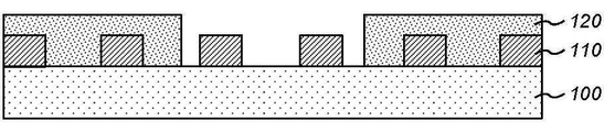
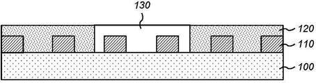
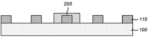
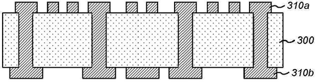
도2a 내지 도2d는 종래기술에 따른 캐비티 제조공법을 나타낸 도면.
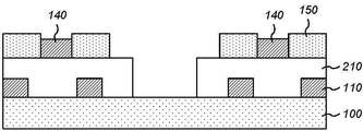
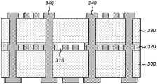
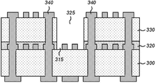
도3a 내지 도3e는 본 발명에 따른 캐비티 제조공법을 나타낸 도면.
Claims (1)
- 회로기판을 제조하는 방법에 있어서,
(a) 절연층 표면에 소정의 회로패턴에 따라 동박이 형성된 코어층을 제작하는 단계;
(b) 상기 코어층의 표면에 PID 층을 피복하고, 캐비티를 제작하고자 하는 부위의 코어층 표면이 노출되도록, 상기 PID 층을 이미지 프로세스를 진행해서 식각함으로써, 소정의 깊이를 지닌 제1 캐비티를 형성하는 단계;
(c) 상기 제1 캐비티가 형성된 PID 층 표면에 노플로우 레진(No Flow Resin) 층을 적층하는 단계; 및
(d) 상기 노플로우 레진층을 레이저로 컷팅하여 소정 부위의 레진층을 따내어서 상기 제1 캐비티 위에 소정의 깊이를 지닌 제2 캐비티를 제작함으로써, 제1 태비티와 제2 캐비티로 구성된 캐비티를 형성하는 단계;
를 포함하는 회로기판 제조방법.
Priority Applications (1)
| Application Number | Priority Date | Filing Date | Title |
|---|---|---|---|
| KR1020150158573A KR20170056042A (ko) | 2015-11-12 | 2015-11-12 | 회로기판 제조방법 |
Applications Claiming Priority (1)
| Application Number | Priority Date | Filing Date | Title |
|---|---|---|---|
| KR1020150158573A KR20170056042A (ko) | 2015-11-12 | 2015-11-12 | 회로기판 제조방법 |
Publications (1)
| Publication Number | Publication Date |
|---|---|
| KR20170056042A true KR20170056042A (ko) | 2017-05-23 |
Family
ID=59050359
Family Applications (1)
| Application Number | Title | Priority Date | Filing Date |
|---|---|---|---|
| KR1020150158573A Ceased KR20170056042A (ko) | 2015-11-12 | 2015-11-12 | 회로기판 제조방법 |
Country Status (1)
| Country | Link |
|---|---|
| KR (1) | KR20170056042A (ko) |
Cited By (2)
| Publication number | Priority date | Publication date | Assignee | Title |
|---|---|---|---|---|
| WO2025190334A1 (zh) * | 2024-03-14 | 2025-09-18 | 四川英创力电子科技股份有限公司 | 一种多阶台阶槽的加工方法及印制电路板 |
| US12501547B2 (en) | 2023-02-09 | 2025-12-16 | Samsung Electro-Mechanics Co., Ltd. | Circuit board and manufacturing method thereof |
-
2015
- 2015-11-12 KR KR1020150158573A patent/KR20170056042A/ko not_active Ceased
Cited By (2)
| Publication number | Priority date | Publication date | Assignee | Title |
|---|---|---|---|---|
| US12501547B2 (en) | 2023-02-09 | 2025-12-16 | Samsung Electro-Mechanics Co., Ltd. | Circuit board and manufacturing method thereof |
| WO2025190334A1 (zh) * | 2024-03-14 | 2025-09-18 | 四川英创力电子科技股份有限公司 | 一种多阶台阶槽的加工方法及印制电路板 |
Similar Documents
| Publication | Publication Date | Title |
|---|---|---|
| US9999134B2 (en) | Self-decap cavity fabrication process and structure | |
| KR100512688B1 (ko) | 캐패시터 내장형 인쇄 회로 기판 제조 방법 | |
| KR101572916B1 (ko) | 연경성회로기판 제조방법 | |
| CN106063393A (zh) | 柔性印刷布线板的制造方法 | |
| JP5464760B2 (ja) | 多層回路基板の製造方法 | |
| CN101287339A (zh) | 制作具有断差结构的电路板的方法 | |
| KR102268388B1 (ko) | 인쇄회로기판 및 그 제조방법 | |
| JP2014093527A (ja) | プリント回路基板の製造方法 | |
| KR100349119B1 (ko) | 인쇄회로기판 및 그 제조방법 | |
| US20170273195A1 (en) | Recessed cavity in printed circuit board protected by lpi | |
| KR101304359B1 (ko) | 캐비티 인쇄회로기판 제조방법 | |
| KR100897668B1 (ko) | 캐리어를 이용한 인쇄회로기판의 제조 방법 | |
| JP4405993B2 (ja) | 高密度プリント回路基板の製造方法 | |
| JP4857433B2 (ja) | 金属積層板、金属積層板の製造方法及び印刷回路基板の製造方法 | |
| KR20090096809A (ko) | 반도체 부품 내장형 인쇄회로기판 제조 방법 | |
| CN101188916A (zh) | 制作具有断差结构的柔性电路板的方法 | |
| JP5302927B2 (ja) | 多層配線基板の製造方法 | |
| US9883599B2 (en) | Manufacturing method for multi-layer circuit board having cavity | |
| KR20170056042A (ko) | 회로기판 제조방법 | |
| JP4617941B2 (ja) | 回路形成基板の製造方法 | |
| KR20170044219A (ko) | 캐비티 회로기판 제조방법 | |
| JP5317491B2 (ja) | プリント配線板の製造方法 | |
| JP2016127248A (ja) | 多層配線基板 | |
| KR101167422B1 (ko) | 캐리어 부재 및 이를 이용한 인쇄회로기판의 제조방법 | |
| KR20090074837A (ko) | 능동 소자 내장을 위한 레이저 캐비티 형성 방법 및 이를적용한 인쇄 회로 기판 |
Legal Events
| Date | Code | Title | Description |
|---|---|---|---|
| A201 | Request for examination | ||
| PA0109 | Patent application |
Patent event code: PA01091R01D Comment text: Patent Application Patent event date: 20151112 |
|
| PA0201 | Request for examination | ||
| E902 | Notification of reason for refusal | ||
| PE0902 | Notice of grounds for rejection |
Comment text: Notification of reason for refusal Patent event date: 20161128 Patent event code: PE09021S01D |
|
| E601 | Decision to refuse application | ||
| PE0601 | Decision on rejection of patent |
Patent event date: 20170427 Comment text: Decision to Refuse Application Patent event code: PE06012S01D Patent event date: 20161128 Comment text: Notification of reason for refusal Patent event code: PE06011S01I |
|
| PG1501 | Laying open of application |