KR20170056445A - 적층체 및 합동체·반도체 장치의 제조 방법 - Google Patents
적층체 및 합동체·반도체 장치의 제조 방법 Download PDFInfo
- Publication number
- KR20170056445A KR20170056445A KR1020160148541A KR20160148541A KR20170056445A KR 20170056445 A KR20170056445 A KR 20170056445A KR 1020160148541 A KR1020160148541 A KR 1020160148541A KR 20160148541 A KR20160148541 A KR 20160148541A KR 20170056445 A KR20170056445 A KR 20170056445A
- Authority
- KR
- South Korea
- Prior art keywords
- semiconductor
- protective film
- resin
- backside protective
- dicing
- Prior art date
- Legal status (The legal status is an assumption and is not a legal conclusion. Google has not performed a legal analysis and makes no representation as to the accuracy of the status listed.)
- Granted
Links
Images



Classifications
-
- B—PERFORMING OPERATIONS; TRANSPORTING
- B32—LAYERED PRODUCTS
- B32B—LAYERED PRODUCTS, i.e. PRODUCTS BUILT-UP OF STRATA OF FLAT OR NON-FLAT, e.g. CELLULAR OR HONEYCOMB, FORM
- B32B27/00—Layered products comprising a layer of synthetic resin
- B32B27/06—Layered products comprising a layer of synthetic resin as the main or only constituent of a layer, which is next to another layer of the same or of a different material
-
- H01L21/6836—
-
- H—ELECTRICITY
- H10—SEMICONDUCTOR DEVICES; ELECTRIC SOLID-STATE DEVICES NOT OTHERWISE PROVIDED FOR
- H10P—GENERIC PROCESSES OR APPARATUS FOR THE MANUFACTURE OR TREATMENT OF DEVICES COVERED BY CLASS H10
- H10P72/00—Handling or holding of wafers, substrates or devices during manufacture or treatment thereof
- H10P72/70—Handling or holding of wafers, substrates or devices during manufacture or treatment thereof for supporting or gripping
- H10P72/74—Handling or holding of wafers, substrates or devices during manufacture or treatment thereof for supporting or gripping using temporarily an auxiliary support
- H10P72/7402—Wafer tapes, e.g. grinding or dicing support tapes
-
- B—PERFORMING OPERATIONS; TRANSPORTING
- B32—LAYERED PRODUCTS
- B32B—LAYERED PRODUCTS, i.e. PRODUCTS BUILT-UP OF STRATA OF FLAT OR NON-FLAT, e.g. CELLULAR OR HONEYCOMB, FORM
- B32B27/00—Layered products comprising a layer of synthetic resin
- B32B27/06—Layered products comprising a layer of synthetic resin as the main or only constituent of a layer, which is next to another layer of the same or of a different material
- B32B27/08—Layered products comprising a layer of synthetic resin as the main or only constituent of a layer, which is next to another layer of the same or of a different material of synthetic resin
-
- B—PERFORMING OPERATIONS; TRANSPORTING
- B32—LAYERED PRODUCTS
- B32B—LAYERED PRODUCTS, i.e. PRODUCTS BUILT-UP OF STRATA OF FLAT OR NON-FLAT, e.g. CELLULAR OR HONEYCOMB, FORM
- B32B27/00—Layered products comprising a layer of synthetic resin
- B32B27/18—Layered products comprising a layer of synthetic resin characterised by the use of special additives
- B32B27/20—Layered products comprising a layer of synthetic resin characterised by the use of special additives using fillers, pigments, thixotroping agents
-
- B—PERFORMING OPERATIONS; TRANSPORTING
- B32—LAYERED PRODUCTS
- B32B—LAYERED PRODUCTS, i.e. PRODUCTS BUILT-UP OF STRATA OF FLAT OR NON-FLAT, e.g. CELLULAR OR HONEYCOMB, FORM
- B32B27/00—Layered products comprising a layer of synthetic resin
- B32B27/30—Layered products comprising a layer of synthetic resin comprising vinyl (co)polymers; comprising acrylic (co)polymers
- B32B27/308—Layered products comprising a layer of synthetic resin comprising vinyl (co)polymers; comprising acrylic (co)polymers comprising acrylic (co)polymers
-
- B—PERFORMING OPERATIONS; TRANSPORTING
- B32—LAYERED PRODUCTS
- B32B—LAYERED PRODUCTS, i.e. PRODUCTS BUILT-UP OF STRATA OF FLAT OR NON-FLAT, e.g. CELLULAR OR HONEYCOMB, FORM
- B32B27/00—Layered products comprising a layer of synthetic resin
- B32B27/36—Layered products comprising a layer of synthetic resin comprising polyesters
-
- B—PERFORMING OPERATIONS; TRANSPORTING
- B32—LAYERED PRODUCTS
- B32B—LAYERED PRODUCTS, i.e. PRODUCTS BUILT-UP OF STRATA OF FLAT OR NON-FLAT, e.g. CELLULAR OR HONEYCOMB, FORM
- B32B27/00—Layered products comprising a layer of synthetic resin
- B32B27/38—Layered products comprising a layer of synthetic resin comprising epoxy resins
-
- B—PERFORMING OPERATIONS; TRANSPORTING
- B32—LAYERED PRODUCTS
- B32B—LAYERED PRODUCTS, i.e. PRODUCTS BUILT-UP OF STRATA OF FLAT OR NON-FLAT, e.g. CELLULAR OR HONEYCOMB, FORM
- B32B27/00—Layered products comprising a layer of synthetic resin
- B32B27/42—Layered products comprising a layer of synthetic resin comprising condensation resins of aldehydes, e.g. with phenols, ureas or melamines
-
- B—PERFORMING OPERATIONS; TRANSPORTING
- B32—LAYERED PRODUCTS
- B32B—LAYERED PRODUCTS, i.e. PRODUCTS BUILT-UP OF STRATA OF FLAT OR NON-FLAT, e.g. CELLULAR OR HONEYCOMB, FORM
- B32B3/00—Layered products comprising a layer with external or internal discontinuities or unevennesses, or a layer of non-planar shape; Layered products comprising a layer having particular features of form
- B32B3/02—Layered products comprising a layer with external or internal discontinuities or unevennesses, or a layer of non-planar shape; Layered products comprising a layer having particular features of form characterised by features of form at particular places, e.g. in edge regions
- B32B3/04—Layered products comprising a layer with external or internal discontinuities or unevennesses, or a layer of non-planar shape; Layered products comprising a layer having particular features of form characterised by features of form at particular places, e.g. in edge regions characterised by at least one layer folded at the edge, e.g. over another layer ; characterised by at least one layer enveloping or enclosing a material
-
- B—PERFORMING OPERATIONS; TRANSPORTING
- B32—LAYERED PRODUCTS
- B32B—LAYERED PRODUCTS, i.e. PRODUCTS BUILT-UP OF STRATA OF FLAT OR NON-FLAT, e.g. CELLULAR OR HONEYCOMB, FORM
- B32B33/00—Layered products characterised by particular properties or particular surface features, e.g. particular surface coatings; Layered products designed for particular purposes not covered by another single class
-
- B—PERFORMING OPERATIONS; TRANSPORTING
- B32—LAYERED PRODUCTS
- B32B—LAYERED PRODUCTS, i.e. PRODUCTS BUILT-UP OF STRATA OF FLAT OR NON-FLAT, e.g. CELLULAR OR HONEYCOMB, FORM
- B32B7/00—Layered products characterised by the relation between layers; Layered products characterised by the relative orientation of features between layers, or by the relative values of a measurable parameter between layers, i.e. products comprising layers having different physical, chemical or physicochemical properties; Layered products characterised by the interconnection of layers
- B32B7/04—Interconnection of layers
- B32B7/06—Interconnection of layers permitting easy separation
-
- B—PERFORMING OPERATIONS; TRANSPORTING
- B32—LAYERED PRODUCTS
- B32B—LAYERED PRODUCTS, i.e. PRODUCTS BUILT-UP OF STRATA OF FLAT OR NON-FLAT, e.g. CELLULAR OR HONEYCOMB, FORM
- B32B7/00—Layered products characterised by the relation between layers; Layered products characterised by the relative orientation of features between layers, or by the relative values of a measurable parameter between layers, i.e. products comprising layers having different physical, chemical or physicochemical properties; Layered products characterised by the interconnection of layers
- B32B7/04—Interconnection of layers
- B32B7/10—Interconnection of layers at least one layer having inter-reactive properties
-
- B—PERFORMING OPERATIONS; TRANSPORTING
- B32—LAYERED PRODUCTS
- B32B—LAYERED PRODUCTS, i.e. PRODUCTS BUILT-UP OF STRATA OF FLAT OR NON-FLAT, e.g. CELLULAR OR HONEYCOMB, FORM
- B32B7/00—Layered products characterised by the relation between layers; Layered products characterised by the relative orientation of features between layers, or by the relative values of a measurable parameter between layers, i.e. products comprising layers having different physical, chemical or physicochemical properties; Layered products characterised by the interconnection of layers
- B32B7/04—Interconnection of layers
- B32B7/12—Interconnection of layers using interposed adhesives or interposed materials with bonding properties
-
- C—CHEMISTRY; METALLURGY
- C08—ORGANIC MACROMOLECULAR COMPOUNDS; THEIR PREPARATION OR CHEMICAL WORKING-UP; COMPOSITIONS BASED THEREON
- C08J—WORKING-UP; GENERAL PROCESSES OF COMPOUNDING; AFTER-TREATMENT NOT COVERED BY SUBCLASSES C08B, C08C, C08F, C08G or C08H
- C08J7/00—Chemical treatment or coating of shaped articles made of macromolecular substances
- C08J7/04—Coating
- C08J7/0427—Coating with only one layer of a composition containing a polymer binder
-
- C—CHEMISTRY; METALLURGY
- C09—DYES; PAINTS; POLISHES; NATURAL RESINS; ADHESIVES; COMPOSITIONS NOT OTHERWISE PROVIDED FOR; APPLICATIONS OF MATERIALS NOT OTHERWISE PROVIDED FOR
- C09D—COATING COMPOSITIONS, e.g. PAINTS, VARNISHES OR LACQUERS; FILLING PASTES; CHEMICAL PAINT OR INK REMOVERS; INKS; CORRECTING FLUIDS; WOODSTAINS; PASTES OR SOLIDS FOR COLOURING OR PRINTING; USE OF MATERIALS THEREFOR
- C09D161/00—Coating compositions based on condensation polymers of aldehydes or ketones; Coating compositions based on derivatives of such polymers
- C09D161/04—Condensation polymers of aldehydes or ketones with phenols only
- C09D161/06—Condensation polymers of aldehydes or ketones with phenols only of aldehydes with phenols
-
- C—CHEMISTRY; METALLURGY
- C09—DYES; PAINTS; POLISHES; NATURAL RESINS; ADHESIVES; COMPOSITIONS NOT OTHERWISE PROVIDED FOR; APPLICATIONS OF MATERIALS NOT OTHERWISE PROVIDED FOR
- C09D—COATING COMPOSITIONS, e.g. PAINTS, VARNISHES OR LACQUERS; FILLING PASTES; CHEMICAL PAINT OR INK REMOVERS; INKS; CORRECTING FLUIDS; WOODSTAINS; PASTES OR SOLIDS FOR COLOURING OR PRINTING; USE OF MATERIALS THEREFOR
- C09D7/00—Features of coating compositions, not provided for in group C09D5/00; Processes for incorporating ingredients in coating compositions
- C09D7/40—Additives
- C09D7/70—Additives characterised by shape, e.g. fibres, flakes or microspheres
-
- H01L21/324—
-
- H01L21/56—
-
- H01L21/67098—
-
- H01L21/78—
-
- H—ELECTRICITY
- H10—SEMICONDUCTOR DEVICES; ELECTRIC SOLID-STATE DEVICES NOT OTHERWISE PROVIDED FOR
- H10P—GENERIC PROCESSES OR APPARATUS FOR THE MANUFACTURE OR TREATMENT OF DEVICES COVERED BY CLASS H10
- H10P54/00—Cutting or separating of wafers, substrates or parts of devices
-
- H—ELECTRICITY
- H10—SEMICONDUCTOR DEVICES; ELECTRIC SOLID-STATE DEVICES NOT OTHERWISE PROVIDED FOR
- H10P—GENERIC PROCESSES OR APPARATUS FOR THE MANUFACTURE OR TREATMENT OF DEVICES COVERED BY CLASS H10
- H10P72/00—Handling or holding of wafers, substrates or devices during manufacture or treatment thereof
- H10P72/04—Apparatus for manufacture or treatment
- H10P72/0431—Apparatus for thermal treatment
-
- H—ELECTRICITY
- H10—SEMICONDUCTOR DEVICES; ELECTRIC SOLID-STATE DEVICES NOT OTHERWISE PROVIDED FOR
- H10P—GENERIC PROCESSES OR APPARATUS FOR THE MANUFACTURE OR TREATMENT OF DEVICES COVERED BY CLASS H10
- H10P72/00—Handling or holding of wafers, substrates or devices during manufacture or treatment thereof
- H10P72/70—Handling or holding of wafers, substrates or devices during manufacture or treatment thereof for supporting or gripping
- H10P72/74—Handling or holding of wafers, substrates or devices during manufacture or treatment thereof for supporting or gripping using temporarily an auxiliary support
- H10P72/7402—Wafer tapes, e.g. grinding or dicing support tapes
- H10P72/7404—Wafer tapes, e.g. grinding or dicing support tapes the wafer tape being a laminate of three or more layers, e.g. including additional layers beyond a base layer and an uppermost adhesive layer
-
- H—ELECTRICITY
- H10—SEMICONDUCTOR DEVICES; ELECTRIC SOLID-STATE DEVICES NOT OTHERWISE PROVIDED FOR
- H10P—GENERIC PROCESSES OR APPARATUS FOR THE MANUFACTURE OR TREATMENT OF DEVICES COVERED BY CLASS H10
- H10P95/00—Generic processes or apparatus for manufacture or treatments not covered by the other groups of this subclass
- H10P95/90—Thermal treatments, e.g. annealing or sintering
-
- H—ELECTRICITY
- H10—SEMICONDUCTOR DEVICES; ELECTRIC SOLID-STATE DEVICES NOT OTHERWISE PROVIDED FOR
- H10W—GENERIC PACKAGES, INTERCONNECTIONS, CONNECTORS OR OTHER CONSTRUCTIONAL DETAILS OF DEVICES COVERED BY CLASS H10
- H10W72/00—Interconnections or connectors in packages
-
- H—ELECTRICITY
- H10—SEMICONDUCTOR DEVICES; ELECTRIC SOLID-STATE DEVICES NOT OTHERWISE PROVIDED FOR
- H10W—GENERIC PACKAGES, INTERCONNECTIONS, CONNECTORS OR OTHER CONSTRUCTIONAL DETAILS OF DEVICES COVERED BY CLASS H10
- H10W74/00—Encapsulations, e.g. protective coatings
- H10W74/01—Manufacture or treatment
-
- B—PERFORMING OPERATIONS; TRANSPORTING
- B32—LAYERED PRODUCTS
- B32B—LAYERED PRODUCTS, i.e. PRODUCTS BUILT-UP OF STRATA OF FLAT OR NON-FLAT, e.g. CELLULAR OR HONEYCOMB, FORM
- B32B2250/00—Layers arrangement
- B32B2250/44—Number of layers variable across the laminate
-
- B—PERFORMING OPERATIONS; TRANSPORTING
- B32—LAYERED PRODUCTS
- B32B—LAYERED PRODUCTS, i.e. PRODUCTS BUILT-UP OF STRATA OF FLAT OR NON-FLAT, e.g. CELLULAR OR HONEYCOMB, FORM
- B32B2255/00—Coating on the layer surface
- B32B2255/26—Polymeric coating
-
- B—PERFORMING OPERATIONS; TRANSPORTING
- B32—LAYERED PRODUCTS
- B32B—LAYERED PRODUCTS, i.e. PRODUCTS BUILT-UP OF STRATA OF FLAT OR NON-FLAT, e.g. CELLULAR OR HONEYCOMB, FORM
- B32B2264/00—Composition or properties of particles which form a particulate layer or are present as additives
- B32B2264/10—Inorganic particles
-
- B—PERFORMING OPERATIONS; TRANSPORTING
- B32—LAYERED PRODUCTS
- B32B—LAYERED PRODUCTS, i.e. PRODUCTS BUILT-UP OF STRATA OF FLAT OR NON-FLAT, e.g. CELLULAR OR HONEYCOMB, FORM
- B32B2307/00—Properties of the layers or laminate
- B32B2307/20—Properties of the layers or laminate having particular electrical or magnetic properties, e.g. piezoelectric
- B32B2307/202—Conductive
-
- B—PERFORMING OPERATIONS; TRANSPORTING
- B32—LAYERED PRODUCTS
- B32B—LAYERED PRODUCTS, i.e. PRODUCTS BUILT-UP OF STRATA OF FLAT OR NON-FLAT, e.g. CELLULAR OR HONEYCOMB, FORM
- B32B2307/00—Properties of the layers or laminate
- B32B2307/50—Properties of the layers or laminate having particular mechanical properties
- B32B2307/54—Yield strength; Tensile strength
-
- B—PERFORMING OPERATIONS; TRANSPORTING
- B32—LAYERED PRODUCTS
- B32B—LAYERED PRODUCTS, i.e. PRODUCTS BUILT-UP OF STRATA OF FLAT OR NON-FLAT, e.g. CELLULAR OR HONEYCOMB, FORM
- B32B2307/00—Properties of the layers or laminate
- B32B2307/70—Other properties
- B32B2307/748—Releasability
-
- B—PERFORMING OPERATIONS; TRANSPORTING
- B32—LAYERED PRODUCTS
- B32B—LAYERED PRODUCTS, i.e. PRODUCTS BUILT-UP OF STRATA OF FLAT OR NON-FLAT, e.g. CELLULAR OR HONEYCOMB, FORM
- B32B2398/00—Unspecified macromolecular compounds
- B32B2398/10—Thermosetting resins
-
- B—PERFORMING OPERATIONS; TRANSPORTING
- B32—LAYERED PRODUCTS
- B32B—LAYERED PRODUCTS, i.e. PRODUCTS BUILT-UP OF STRATA OF FLAT OR NON-FLAT, e.g. CELLULAR OR HONEYCOMB, FORM
- B32B2398/00—Unspecified macromolecular compounds
- B32B2398/20—Thermoplastics
-
- B—PERFORMING OPERATIONS; TRANSPORTING
- B32—LAYERED PRODUCTS
- B32B—LAYERED PRODUCTS, i.e. PRODUCTS BUILT-UP OF STRATA OF FLAT OR NON-FLAT, e.g. CELLULAR OR HONEYCOMB, FORM
- B32B2457/00—Electrical equipment
- B32B2457/14—Semiconductor wafers
-
- C—CHEMISTRY; METALLURGY
- C08—ORGANIC MACROMOLECULAR COMPOUNDS; THEIR PREPARATION OR CHEMICAL WORKING-UP; COMPOSITIONS BASED THEREON
- C08J—WORKING-UP; GENERAL PROCESSES OF COMPOUNDING; AFTER-TREATMENT NOT COVERED BY SUBCLASSES C08B, C08C, C08F, C08G or C08H
- C08J2367/00—Characterised by the use of polyesters obtained by reactions forming a carboxylic ester link in the main chain; Derivatives of such polymers
- C08J2367/02—Polyesters derived from dicarboxylic acids and dihydroxy compounds
-
- C—CHEMISTRY; METALLURGY
- C08—ORGANIC MACROMOLECULAR COMPOUNDS; THEIR PREPARATION OR CHEMICAL WORKING-UP; COMPOSITIONS BASED THEREON
- C08J—WORKING-UP; GENERAL PROCESSES OF COMPOUNDING; AFTER-TREATMENT NOT COVERED BY SUBCLASSES C08B, C08C, C08F, C08G or C08H
- C08J2461/00—Characterised by the use of condensation polymers of aldehydes or ketones; Derivatives of such polymers
- C08J2461/04—Condensation polymers of aldehydes or ketones with phenols only
- C08J2461/06—Condensation polymers of aldehydes or ketones with phenols only of aldehydes with phenols
-
- C—CHEMISTRY; METALLURGY
- C08—ORGANIC MACROMOLECULAR COMPOUNDS; THEIR PREPARATION OR CHEMICAL WORKING-UP; COMPOSITIONS BASED THEREON
- C08L—COMPOSITIONS OF MACROMOLECULAR COMPOUNDS
- C08L2203/00—Applications
- C08L2203/16—Applications used for films
-
- C—CHEMISTRY; METALLURGY
- C08—ORGANIC MACROMOLECULAR COMPOUNDS; THEIR PREPARATION OR CHEMICAL WORKING-UP; COMPOSITIONS BASED THEREON
- C08L—COMPOSITIONS OF MACROMOLECULAR COMPOUNDS
- C08L2205/00—Polymer mixtures characterised by other features
- C08L2205/02—Polymer mixtures characterised by other features containing two or more polymers of the same C08L -group
- C08L2205/025—Polymer mixtures characterised by other features containing two or more polymers of the same C08L -group containing two or more polymers of the same hierarchy C08L, and differing only in parameters such as density, comonomer content, molecular weight, structure
-
- C—CHEMISTRY; METALLURGY
- C08—ORGANIC MACROMOLECULAR COMPOUNDS; THEIR PREPARATION OR CHEMICAL WORKING-UP; COMPOSITIONS BASED THEREON
- C08L—COMPOSITIONS OF MACROMOLECULAR COMPOUNDS
- C08L2205/00—Polymer mixtures characterised by other features
- C08L2205/03—Polymer mixtures characterised by other features containing three or more polymers in a blend
- C08L2205/035—Polymer mixtures characterised by other features containing three or more polymers in a blend containing four or more polymers in a blend
-
- H01L2924/0635—
-
- H01L2924/066—
-
- H01L2924/0665—
-
- H—ELECTRICITY
- H10—SEMICONDUCTOR DEVICES; ELECTRIC SOLID-STATE DEVICES NOT OTHERWISE PROVIDED FOR
- H10P—GENERIC PROCESSES OR APPARATUS FOR THE MANUFACTURE OR TREATMENT OF DEVICES COVERED BY CLASS H10
- H10P72/00—Handling or holding of wafers, substrates or devices during manufacture or treatment thereof
- H10P72/70—Handling or holding of wafers, substrates or devices during manufacture or treatment thereof for supporting or gripping
- H10P72/74—Handling or holding of wafers, substrates or devices during manufacture or treatment thereof for supporting or gripping using temporarily an auxiliary support
- H10P72/7416—Handling or holding of wafers, substrates or devices during manufacture or treatment thereof for supporting or gripping using temporarily an auxiliary support used during dicing or grinding
-
- H—ELECTRICITY
- H10—SEMICONDUCTOR DEVICES; ELECTRIC SOLID-STATE DEVICES NOT OTHERWISE PROVIDED FOR
- H10P—GENERIC PROCESSES OR APPARATUS FOR THE MANUFACTURE OR TREATMENT OF DEVICES COVERED BY CLASS H10
- H10P72/00—Handling or holding of wafers, substrates or devices during manufacture or treatment thereof
- H10P72/70—Handling or holding of wafers, substrates or devices during manufacture or treatment thereof for supporting or gripping
- H10P72/74—Handling or holding of wafers, substrates or devices during manufacture or treatment thereof for supporting or gripping using temporarily an auxiliary support
- H10P72/7438—Handling or holding of wafers, substrates or devices during manufacture or treatment thereof for supporting or gripping using temporarily an auxiliary support with parts of the auxiliary support remaining in the finished device
-
- H—ELECTRICITY
- H10—SEMICONDUCTOR DEVICES; ELECTRIC SOLID-STATE DEVICES NOT OTHERWISE PROVIDED FOR
- H10W—GENERIC PACKAGES, INTERCONNECTIONS, CONNECTORS OR OTHER CONSTRUCTIONAL DETAILS OF DEVICES COVERED BY CLASS H10
- H10W42/00—Arrangements for protection of devices
- H10W42/121—Arrangements for protection of devices protecting against mechanical damage
-
- H—ELECTRICITY
- H10—SEMICONDUCTOR DEVICES; ELECTRIC SOLID-STATE DEVICES NOT OTHERWISE PROVIDED FOR
- H10W—GENERIC PACKAGES, INTERCONNECTIONS, CONNECTORS OR OTHER CONSTRUCTIONAL DETAILS OF DEVICES COVERED BY CLASS H10
- H10W46/00—Marks applied to devices, e.g. for alignment or identification
-
- H—ELECTRICITY
- H10—SEMICONDUCTOR DEVICES; ELECTRIC SOLID-STATE DEVICES NOT OTHERWISE PROVIDED FOR
- H10W—GENERIC PACKAGES, INTERCONNECTIONS, CONNECTORS OR OTHER CONSTRUCTIONAL DETAILS OF DEVICES COVERED BY CLASS H10
- H10W46/00—Marks applied to devices, e.g. for alignment or identification
- H10W46/601—Marks applied to devices, e.g. for alignment or identification for use after dicing
- H10W46/607—Located on parts of packages, e.g. on encapsulations or on package substrates
-
- H—ELECTRICITY
- H10—SEMICONDUCTOR DEVICES; ELECTRIC SOLID-STATE DEVICES NOT OTHERWISE PROVIDED FOR
- H10W—GENERIC PACKAGES, INTERCONNECTIONS, CONNECTORS OR OTHER CONSTRUCTIONAL DETAILS OF DEVICES COVERED BY CLASS H10
- H10W72/00—Interconnections or connectors in packages
- H10W72/20—Bump connectors, e.g. solder bumps or copper pillars; Dummy bumps; Thermal bumps
- H10W72/251—Materials
- H10W72/252—Materials comprising solid metals or solid metalloids, e.g. PbSn, Ag or Cu
-
- H—ELECTRICITY
- H10—SEMICONDUCTOR DEVICES; ELECTRIC SOLID-STATE DEVICES NOT OTHERWISE PROVIDED FOR
- H10W—GENERIC PACKAGES, INTERCONNECTIONS, CONNECTORS OR OTHER CONSTRUCTIONAL DETAILS OF DEVICES COVERED BY CLASS H10
- H10W72/00—Interconnections or connectors in packages
- H10W72/90—Bond pads, in general
- H10W72/951—Materials of bond pads
- H10W72/952—Materials of bond pads comprising metals or metalloids, e.g. PbSn, Ag or Cu
-
- H—ELECTRICITY
- H10—SEMICONDUCTOR DEVICES; ELECTRIC SOLID-STATE DEVICES NOT OTHERWISE PROVIDED FOR
- H10W—GENERIC PACKAGES, INTERCONNECTIONS, CONNECTORS OR OTHER CONSTRUCTIONAL DETAILS OF DEVICES COVERED BY CLASS H10
- H10W90/00—Package configurations
- H10W90/701—Package configurations characterised by the relative positions of pads or connectors relative to package parts
- H10W90/721—Package configurations characterised by the relative positions of pads or connectors relative to package parts of bump connectors
- H10W90/724—Package configurations characterised by the relative positions of pads or connectors relative to package parts of bump connectors between a chip and a stacked insulating package substrate, interposer or RDL
-
- H—ELECTRICITY
- H10—SEMICONDUCTOR DEVICES; ELECTRIC SOLID-STATE DEVICES NOT OTHERWISE PROVIDED FOR
- H10W—GENERIC PACKAGES, INTERCONNECTIONS, CONNECTORS OR OTHER CONSTRUCTIONAL DETAILS OF DEVICES COVERED BY CLASS H10
- H10W90/00—Package configurations
- H10W90/701—Package configurations characterised by the relative positions of pads or connectors relative to package parts
- H10W90/721—Package configurations characterised by the relative positions of pads or connectors relative to package parts of bump connectors
- H10W90/726—Package configurations characterised by the relative positions of pads or connectors relative to package parts of bump connectors between a chip and a stacked lead frame, conducting package substrate or heat sink
Landscapes
- Chemical & Material Sciences (AREA)
- Organic Chemistry (AREA)
- Wood Science & Technology (AREA)
- Life Sciences & Earth Sciences (AREA)
- Engineering & Computer Science (AREA)
- Materials Engineering (AREA)
- Medicinal Chemistry (AREA)
- Polymers & Plastics (AREA)
- Chemical Kinetics & Catalysis (AREA)
- Health & Medical Sciences (AREA)
- Dicing (AREA)
- Adhesive Tapes (AREA)
- Laminated Bodies (AREA)
- Container, Conveyance, Adherence, Positioning, Of Wafer (AREA)
- Adhesives Or Adhesive Processes (AREA)
Abstract
다이싱 시트와 반도체 이면 보호 필름을 포함하는 적층체에 관한 것이다. 다이싱 시트는, 기재층과, 기재층 상에 배치된 점착제층을 포함한다. 반도체 이면 보호 필름은 점착제층 상에 배치되어 있다. 경화 후에 있어서의 반도체 이면 보호 필름의 인장 저장 탄성률은 23℃ 내지 80℃의 전 범위에서 1㎬ 이상이다.
Description
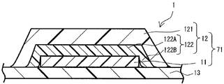
도 2는 합동체의 일부의 개략 단면도이다.
도 3은 반도체 장치의 제조 공정의 개략 단면도이다.
도 4는 반도체 장치의 제조 공정의 개략 단면도이다.
도 5는 반도체 장치의 제조 공정의 개략 단면도이다.
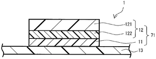
도 6은 변형예 1에 있어서의 적층체의 개략 단면도이다.
도 7은 적층체와, 적층체에 고정된 웨이퍼의 개략 단면도이며, 다이싱 블레이드의 절입 깊이를 나타낸 것이다.
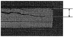
도 8은 실시예에 있어서의 조합-실리콘 칩과 다이싱 후 반도체 이면 보호 필름을 포함함-의 측면도이며, 균열의 깊이를 나타낸 것이다.

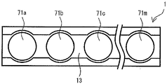
11: 반도체 이면 보호 필름
12: 다이싱 시트
121: 기재층
122: 점착제층
122A: 제1 부분
122B: 제2 부분
13: 박리 라이너
71: 적층체
4: 반도체 웨이퍼
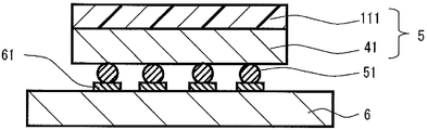
5: 조합
6: 피착체
8: 흡착대
41: 반도체 칩
51: 범프
61: 도전재
111: 다이싱 후 반도체 이면 보호 필름
Claims (5)
- 기재층 및 상기 기재층 상에 배치된 점착제층을 포함하는 다이싱 시트와,
상기 점착제층 상에 배치된 반도체 이면 보호 필름을 포함하고,
경화 후에 있어서의 상기 반도체 이면 보호 필름의 인장 저장 탄성률이 23℃ 내지 80℃의 전 범위에서 1㎬ 이상인, 적층체. - 제1항에 있어서,
경화 후에 있어서의 상기 반도체 이면 보호 필름의 80℃ 인장 저장 탄성률의, 경화 후에 있어서의 상기 반도체 이면 보호 필름의 23℃ 인장 저장 탄성률에 대한 비가 0.3 내지 1.0인, 적층체. - 제1항에 있어서,
상기 반도체 이면 보호 필름은 수지 성분을 포함하고,
상기 수지 성분은, 아크릴 수지, 에폭시 수지 및 페놀 수지를 포함하며,
상기 수지 성분 100중량% 중에 있어서의 상기 아크릴 수지의 함유량은 0.1중량% 내지 30중량%인, 적층체. - 박리 라이너와,
상기 박리 라이너 상에 배치된, 제1항에 기재된 적층체를 포함하는 합동체. - 제1항 내지 제3항 중 어느 한 항에 기재된 적층체의 상기 반도체 이면 보호 필름에 반도체 웨이퍼를 고정하는 공정과,
상기 적층체의 상기 반도체 이면 보호 필름에 상기 반도체 웨이퍼를 고정하는 공정 후에, 상기 반도체 이면 보호 필름을 경화시키는 공정과,
상기 반도체 이면 보호 필름을 경화시키는 공정 후에, 상기 반도체 이면 보호 필름에 고정된 상기 반도체 웨이퍼를 다이싱함으로써, 반도체 칩, 및 상기 반도체 칩에 고정된 다이싱 후 반도체 이면 보호 필름을 포함하는 조합을 형성하는 공정과,
상기 다이싱 시트로부터 상기 조합을 박리하는 공정을 포함하는 반도체 장치의 제조 방법.
Applications Claiming Priority (2)
| Application Number | Priority Date | Filing Date | Title |
|---|---|---|---|
| JP2015222896A JP6660156B2 (ja) | 2015-11-13 | 2015-11-13 | 積層体および合同体・半導体装置の製造方法 |
| JPJP-P-2015-222896 | 2015-11-13 |
Publications (2)
| Publication Number | Publication Date |
|---|---|
| KR20170056445A true KR20170056445A (ko) | 2017-05-23 |
| KR102559864B1 KR102559864B1 (ko) | 2023-07-27 |
Family
ID=58691309
Family Applications (1)
| Application Number | Title | Priority Date | Filing Date |
|---|---|---|---|
| KR1020160148541A Active KR102559864B1 (ko) | 2015-11-13 | 2016-11-09 | 적층체 및 합동체·반도체 장치의 제조 방법 |
Country Status (5)
| Country | Link |
|---|---|
| US (1) | US20170140973A1 (ko) |
| JP (1) | JP6660156B2 (ko) |
| KR (1) | KR102559864B1 (ko) |
| CN (1) | CN106696408B (ko) |
| TW (1) | TWI710462B (ko) |
Families Citing this family (5)
| Publication number | Priority date | Publication date | Assignee | Title |
|---|---|---|---|---|
| CN120003120A (zh) * | 2017-03-17 | 2025-05-16 | 汉高股份有限及两合公司 | 多层制品的工作寿命改善及其制备方法和用途 |
| JP6921644B2 (ja) * | 2017-06-27 | 2021-08-18 | 日東電工株式会社 | ダイシングテープ一体型裏面保護フィルム |
| KR102929203B1 (ko) * | 2018-11-22 | 2026-02-20 | 린텍 가부시키가이샤 | 열경화성 보호막 형성용 필름, 보호막 형성용 복합 시트, 및 칩의 제조 방법 |
| CN113841223B (zh) * | 2019-05-23 | 2024-02-06 | 三菱电机株式会社 | 半导体基板的制造方法和半导体装置的制造方法 |
| TW202323359A (zh) * | 2021-07-21 | 2023-06-16 | 德商漢高智慧財產控股公司 | 用於具有優異高溫性質之供3d矽穿孔(tsv)封裝用之非傳導性薄膜的樹脂組合物 |
Citations (6)
| Publication number | Priority date | Publication date | Assignee | Title |
|---|---|---|---|---|
| JP2009256466A (ja) * | 2008-04-16 | 2009-11-05 | Sekisui Chem Co Ltd | 電子部品用接着剤 |
| JP2010199541A (ja) | 2009-01-30 | 2010-09-09 | Nitto Denko Corp | ダイシングテープ一体型ウエハ裏面保護フィルム |
| JP2012169482A (ja) * | 2011-02-15 | 2012-09-06 | Nitto Denko Corp | 保護層形成用フィルム |
| KR20130036158A (ko) * | 2011-10-03 | 2013-04-11 | 닛토덴코 가부시키가이샤 | 열점착성 필름 및 점착 테이프 |
| KR20130056861A (ko) * | 2010-04-19 | 2013-05-30 | 닛토덴코 가부시키가이샤 | 플립칩형 반도체 이면용 필름 |
| KR20150094581A (ko) * | 2010-07-29 | 2015-08-19 | 닛토덴코 가부시키가이샤 | 플립 칩형 반도체 이면용 필름 및 그의 용도 |
Family Cites Families (5)
| Publication number | Priority date | Publication date | Assignee | Title |
|---|---|---|---|---|
| JP4642436B2 (ja) * | 2004-11-12 | 2011-03-02 | リンテック株式会社 | マーキング方法および保護膜形成兼ダイシング用シート |
| JP2008166451A (ja) * | 2006-12-27 | 2008-07-17 | Furukawa Electric Co Ltd:The | チップ保護用フィルム |
| JP5632695B2 (ja) * | 2009-11-26 | 2014-11-26 | 日東電工株式会社 | ダイシングフィルム付き接着フィルム、及び、該ダイシングフィルム付き接着フィルムを用いた半導体装置の製造方法 |
| JP6001273B2 (ja) * | 2012-02-13 | 2016-10-05 | 信越化学工業株式会社 | 半導体ウエハ用保護フィルム及び半導体チップの製造方法 |
| KR20150135284A (ko) * | 2013-03-22 | 2015-12-02 | 린텍 가부시키가이샤 | 보호막 형성용 필름 및 보호막 형성용 복합 시트 |
-
2015
- 2015-11-13 JP JP2015222896A patent/JP6660156B2/ja not_active Expired - Fee Related
-
2016
- 2016-11-03 CN CN201610959486.0A patent/CN106696408B/zh not_active Expired - Fee Related
- 2016-11-09 KR KR1020160148541A patent/KR102559864B1/ko active Active
- 2016-11-10 TW TW105136616A patent/TWI710462B/zh not_active IP Right Cessation
- 2016-11-11 US US15/349,169 patent/US20170140973A1/en not_active Abandoned
Patent Citations (6)
| Publication number | Priority date | Publication date | Assignee | Title |
|---|---|---|---|---|
| JP2009256466A (ja) * | 2008-04-16 | 2009-11-05 | Sekisui Chem Co Ltd | 電子部品用接着剤 |
| JP2010199541A (ja) | 2009-01-30 | 2010-09-09 | Nitto Denko Corp | ダイシングテープ一体型ウエハ裏面保護フィルム |
| KR20130056861A (ko) * | 2010-04-19 | 2013-05-30 | 닛토덴코 가부시키가이샤 | 플립칩형 반도체 이면용 필름 |
| KR20150094581A (ko) * | 2010-07-29 | 2015-08-19 | 닛토덴코 가부시키가이샤 | 플립 칩형 반도체 이면용 필름 및 그의 용도 |
| JP2012169482A (ja) * | 2011-02-15 | 2012-09-06 | Nitto Denko Corp | 保護層形成用フィルム |
| KR20130036158A (ko) * | 2011-10-03 | 2013-04-11 | 닛토덴코 가부시키가이샤 | 열점착성 필름 및 점착 테이프 |
Also Published As
| Publication number | Publication date |
|---|---|
| JP2017092333A (ja) | 2017-05-25 |
| TWI710462B (zh) | 2020-11-21 |
| KR102559864B1 (ko) | 2023-07-27 |
| JP6660156B2 (ja) | 2020-03-04 |
| CN106696408B (zh) | 2021-04-13 |
| TW201726421A (zh) | 2017-08-01 |
| CN106696408A (zh) | 2017-05-24 |
| US20170140973A1 (en) | 2017-05-18 |
Similar Documents
| Publication | Publication Date | Title |
|---|---|---|
| KR101516028B1 (ko) | 플립 칩형 반도체 이면용 필름 | |
| KR20170056446A (ko) | 적층체 및 합동체·조합의 회수 방법·반도체 장치의 제조 방법 | |
| TWI605504B (zh) | Flip-chip type semiconductor device manufacturing method | |
| JP6812213B2 (ja) | シート、テープおよび半導体装置の製造方法 | |
| TW201200574A (en) | Dicing tape-integrated film for semiconductor back surface | |
| KR20170056445A (ko) | 적층체 및 합동체·반도체 장치의 제조 방법 | |
| JP2017092335A (ja) | 半導体パッケージの製造方法 | |
| KR101563765B1 (ko) | 플립 칩형 반도체 이면용 필름, 단책상 반도체 이면용 필름의 제조방법, 및 플립 칩형 반도체 장치 | |
| JP6577341B2 (ja) | 積層体および半導体装置の製造方法 | |
| JP2007103954A (ja) | 半導体用接着フィルム、ダイシングフィルムおよび半導体装置 | |
| JP2005032961A (ja) | 半導体用接着フィルム、ダイシングフィルムおよび半導体装置 | |
| KR102444114B1 (ko) | 시트, 테이프, 및 반도체 장치의 제조 방법 | |
| KR102430188B1 (ko) | 시트, 테이프 및 반도체 장치의 제조 방법 | |
| KR20160129756A (ko) | 이면 보호 필름, 필름, 반도체 장치의 제조 방법 및 보호 칩의 제조 방법 | |
| TW202248391A (zh) | 半導體用接著劑、半導體用接著劑片及半導體裝置之製造方法 |
Legal Events
| Date | Code | Title | Description |
|---|---|---|---|
| PA0109 | Patent application |
St.27 status event code: A-0-1-A10-A12-nap-PA0109 |
|
| PG1501 | Laying open of application |
St.27 status event code: A-1-1-Q10-Q12-nap-PG1501 |
|
| A201 | Request for examination | ||
| PA0201 | Request for examination |
St.27 status event code: A-1-2-D10-D11-exm-PA0201 |
|
| D13-X000 | Search requested |
St.27 status event code: A-1-2-D10-D13-srh-X000 |
|
| D14-X000 | Search report completed |
St.27 status event code: A-1-2-D10-D14-srh-X000 |
|
| E902 | Notification of reason for refusal | ||
| PE0902 | Notice of grounds for rejection |
St.27 status event code: A-1-2-D10-D21-exm-PE0902 |
|
| E13-X000 | Pre-grant limitation requested |
St.27 status event code: A-2-3-E10-E13-lim-X000 |
|
| P11-X000 | Amendment of application requested |
St.27 status event code: A-2-2-P10-P11-nap-X000 |
|
| P13-X000 | Application amended |
St.27 status event code: A-2-2-P10-P13-nap-X000 |
|
| E701 | Decision to grant or registration of patent right | ||
| PE0701 | Decision of registration |
St.27 status event code: A-1-2-D10-D22-exm-PE0701 |
|
| PR0701 | Registration of establishment |
St.27 status event code: A-2-4-F10-F11-exm-PR0701 |
|
| PR1002 | Payment of registration fee |
St.27 status event code: A-2-2-U10-U11-oth-PR1002 Fee payment year number: 1 |
|
| PG1601 | Publication of registration |
St.27 status event code: A-4-4-Q10-Q13-nap-PG1601 |
|
| R18-X000 | Changes to party contact information recorded |
St.27 status event code: A-5-5-R10-R18-oth-X000 |
|
| R18-X000 | Changes to party contact information recorded |
St.27 status event code: A-5-5-R10-R18-oth-X000 |
|
| P22-X000 | Classification modified |
St.27 status event code: A-4-4-P10-P22-nap-X000 |