KR20170059971A - 장벽 층을 포함하는 1s1r 메모리 셀 - Google Patents
장벽 층을 포함하는 1s1r 메모리 셀 Download PDFInfo
- Publication number
- KR20170059971A KR20170059971A KR1020177004308A KR20177004308A KR20170059971A KR 20170059971 A KR20170059971 A KR 20170059971A KR 1020177004308 A KR1020177004308 A KR 1020177004308A KR 20177004308 A KR20177004308 A KR 20177004308A KR 20170059971 A KR20170059971 A KR 20170059971A
- Authority
- KR
- South Korea
- Prior art keywords
- oxide
- selector
- barrier
- memory
- depositing
- Prior art date
- Legal status (The legal status is an assumption and is not a legal conclusion. Google has not performed a legal analysis and makes no representation as to the accuracy of the status listed.)
- Granted
Links
- 230000004888 barrier function Effects 0.000 title claims abstract description 157
- 239000000463 material Substances 0.000 claims abstract description 189
- 239000010409 thin film Substances 0.000 claims abstract description 69
- 238000000034 method Methods 0.000 claims abstract description 48
- 239000000203 mixture Substances 0.000 claims abstract description 31
- 229910044991 metal oxide Inorganic materials 0.000 claims abstract description 18
- 150000004706 metal oxides Chemical class 0.000 claims abstract description 17
- 238000000151 deposition Methods 0.000 claims description 54
- 229910052751 metal Inorganic materials 0.000 claims description 39
- 239000002184 metal Substances 0.000 claims description 39
- 239000007772 electrode material Substances 0.000 claims description 28
- 150000001875 compounds Chemical class 0.000 claims description 27
- 239000000758 substrate Substances 0.000 claims description 21
- 238000000231 atomic layer deposition Methods 0.000 claims description 16
- 150000004767 nitrides Chemical class 0.000 claims description 16
- 239000003870 refractory metal Substances 0.000 claims description 16
- 230000007704 transition Effects 0.000 claims description 16
- ITWBWJFEJCHKSN-UHFFFAOYSA-N 1,4,7-triazonane Chemical compound C1CNCCNCCN1 ITWBWJFEJCHKSN-UHFFFAOYSA-N 0.000 claims description 9
- ATJFFYVFTNAWJD-UHFFFAOYSA-N Tin Chemical compound [Sn] ATJFFYVFTNAWJD-UHFFFAOYSA-N 0.000 claims description 9
- 229910052723 transition metal Inorganic materials 0.000 claims description 8
- 150000003624 transition metals Chemical class 0.000 claims description 8
- 230000008569 process Effects 0.000 claims description 7
- 230000003647 oxidation Effects 0.000 claims description 6
- 238000007254 oxidation reaction Methods 0.000 claims description 6
- 238000007667 floating Methods 0.000 claims description 5
- 238000004519 manufacturing process Methods 0.000 claims description 4
- 239000010955 niobium Substances 0.000 claims description 4
- 229910014689 LiMnO Inorganic materials 0.000 claims description 3
- 229910013641 LiNbO 3 Inorganic materials 0.000 claims description 3
- 229910013290 LiNiO 2 Inorganic materials 0.000 claims description 3
- 150000001768 cations Chemical class 0.000 claims description 3
- 229910052735 hafnium Inorganic materials 0.000 claims description 3
- PNEYBMLMFCGWSK-UHFFFAOYSA-N aluminium oxide Inorganic materials [O-2].[O-2].[O-2].[Al+3].[Al+3] PNEYBMLMFCGWSK-UHFFFAOYSA-N 0.000 claims description 2
- 229910052758 niobium Inorganic materials 0.000 claims description 2
- GUCVJGMIXFAOAE-UHFFFAOYSA-N niobium atom Chemical compound [Nb] GUCVJGMIXFAOAE-UHFFFAOYSA-N 0.000 claims description 2
- 229910052720 vanadium Inorganic materials 0.000 claims description 2
- WGLPBDUCMAPZCE-UHFFFAOYSA-N Trioxochromium Chemical compound O=[Cr](=O)=O WGLPBDUCMAPZCE-UHFFFAOYSA-N 0.000 claims 1
- 229910000423 chromium oxide Inorganic materials 0.000 claims 1
- 229910000765 intermetallic Inorganic materials 0.000 claims 1
- BPUBBGLMJRNUCC-UHFFFAOYSA-N oxygen(2-);tantalum(5+) Chemical compound [O-2].[O-2].[O-2].[O-2].[O-2].[Ta+5].[Ta+5] BPUBBGLMJRNUCC-UHFFFAOYSA-N 0.000 claims 1
- 229910001936 tantalum oxide Inorganic materials 0.000 claims 1
- GPPXJZIENCGNKB-UHFFFAOYSA-N vanadium Chemical compound [V]#[V] GPPXJZIENCGNKB-UHFFFAOYSA-N 0.000 claims 1
- 239000003989 dielectric material Substances 0.000 abstract description 18
- 238000006243 chemical reaction Methods 0.000 abstract description 6
- 239000010410 layer Substances 0.000 description 55
- 239000010408 film Substances 0.000 description 19
- 230000006870 function Effects 0.000 description 11
- 238000005240 physical vapour deposition Methods 0.000 description 10
- 238000005516 engineering process Methods 0.000 description 9
- 239000010936 titanium Substances 0.000 description 9
- 238000010586 diagram Methods 0.000 description 8
- 238000009792 diffusion process Methods 0.000 description 7
- 229910003468 tantalcarbide Inorganic materials 0.000 description 7
- 238000005229 chemical vapour deposition Methods 0.000 description 6
- 239000011651 chromium Substances 0.000 description 5
- 230000009286 beneficial effect Effects 0.000 description 4
- 230000008901 benefit Effects 0.000 description 4
- 239000013590 bulk material Substances 0.000 description 4
- 238000005137 deposition process Methods 0.000 description 4
- 229910045601 alloy Inorganic materials 0.000 description 3
- 239000000956 alloy Substances 0.000 description 3
- -1 but not limited to Substances 0.000 description 3
- 150000004770 chalcogenides Chemical group 0.000 description 3
- 230000001965 increasing effect Effects 0.000 description 3
- 239000004065 semiconductor Substances 0.000 description 3
- VYZAMTAEIAYCRO-UHFFFAOYSA-N Chromium Chemical compound [Cr] VYZAMTAEIAYCRO-UHFFFAOYSA-N 0.000 description 2
- RYGMFSIKBFXOCR-UHFFFAOYSA-N Copper Chemical compound [Cu] RYGMFSIKBFXOCR-UHFFFAOYSA-N 0.000 description 2
- PXHVJJICTQNCMI-UHFFFAOYSA-N Nickel Chemical compound [Ni] PXHVJJICTQNCMI-UHFFFAOYSA-N 0.000 description 2
- KDLHZDBZIXYQEI-UHFFFAOYSA-N Palladium Chemical compound [Pd] KDLHZDBZIXYQEI-UHFFFAOYSA-N 0.000 description 2
- RTAQQCXQSZGOHL-UHFFFAOYSA-N Titanium Chemical compound [Ti] RTAQQCXQSZGOHL-UHFFFAOYSA-N 0.000 description 2
- 150000001450 anions Chemical class 0.000 description 2
- 230000002457 bidirectional effect Effects 0.000 description 2
- 229910052804 chromium Inorganic materials 0.000 description 2
- 238000004891 communication Methods 0.000 description 2
- 238000007796 conventional method Methods 0.000 description 2
- 229910052802 copper Inorganic materials 0.000 description 2
- 239000010949 copper Substances 0.000 description 2
- VBJZVLUMGGDVMO-UHFFFAOYSA-N hafnium atom Chemical compound [Hf] VBJZVLUMGGDVMO-UHFFFAOYSA-N 0.000 description 2
- 230000004048 modification Effects 0.000 description 2
- 238000012986 modification Methods 0.000 description 2
- 230000003287 optical effect Effects 0.000 description 2
- 239000007800 oxidant agent Substances 0.000 description 2
- 230000001590 oxidative effect Effects 0.000 description 2
- BASFCYQUMIYNBI-UHFFFAOYSA-N platinum Chemical compound [Pt] BASFCYQUMIYNBI-UHFFFAOYSA-N 0.000 description 2
- 238000012545 processing Methods 0.000 description 2
- 230000004044 response Effects 0.000 description 2
- 239000002356 single layer Substances 0.000 description 2
- 239000007787 solid Substances 0.000 description 2
- 229910052715 tantalum Inorganic materials 0.000 description 2
- GUVRBAGPIYLISA-UHFFFAOYSA-N tantalum atom Chemical compound [Ta] GUVRBAGPIYLISA-UHFFFAOYSA-N 0.000 description 2
- 229910052719 titanium Inorganic materials 0.000 description 2
- 150000003623 transition metal compounds Chemical class 0.000 description 2
- 229910000314 transition metal oxide Inorganic materials 0.000 description 2
- 229910052721 tungsten Inorganic materials 0.000 description 2
- 239000010937 tungsten Substances 0.000 description 2
- LEONUFNNVUYDNQ-UHFFFAOYSA-N vanadium atom Chemical compound [V] LEONUFNNVUYDNQ-UHFFFAOYSA-N 0.000 description 2
- 229910052726 zirconium Inorganic materials 0.000 description 2
- OKTJSMMVPCPJKN-UHFFFAOYSA-N Carbon Chemical compound [C] OKTJSMMVPCPJKN-UHFFFAOYSA-N 0.000 description 1
- 229910002531 CuTe Inorganic materials 0.000 description 1
- 229910000577 Silicon-germanium Inorganic materials 0.000 description 1
- 229910010413 TiO 2 Inorganic materials 0.000 description 1
- NRTOMJZYCJJWKI-UHFFFAOYSA-N Titanium nitride Chemical compound [Ti]#N NRTOMJZYCJJWKI-UHFFFAOYSA-N 0.000 description 1
- QCWXUUIWCKQGHC-UHFFFAOYSA-N Zirconium Chemical compound [Zr] QCWXUUIWCKQGHC-UHFFFAOYSA-N 0.000 description 1
- 230000004913 activation Effects 0.000 description 1
- 230000004075 alteration Effects 0.000 description 1
- 238000003491 array Methods 0.000 description 1
- 238000000429 assembly Methods 0.000 description 1
- 230000000712 assembly Effects 0.000 description 1
- 230000005540 biological transmission Effects 0.000 description 1
- 230000015572 biosynthetic process Effects 0.000 description 1
- 229910052799 carbon Inorganic materials 0.000 description 1
- 230000008859 change Effects 0.000 description 1
- 239000004020 conductor Substances 0.000 description 1
- 230000008021 deposition Effects 0.000 description 1
- 230000001627 detrimental effect Effects 0.000 description 1
- 238000011161 development Methods 0.000 description 1
- 239000002355 dual-layer Substances 0.000 description 1
- 230000005684 electric field Effects 0.000 description 1
- 238000007772 electroless plating Methods 0.000 description 1
- 238000009713 electroplating Methods 0.000 description 1
- 229910001325 element alloy Inorganic materials 0.000 description 1
- 229910052732 germanium Inorganic materials 0.000 description 1
- GNPVGFCGXDBREM-UHFFFAOYSA-N germanium atom Chemical compound [Ge] GNPVGFCGXDBREM-UHFFFAOYSA-N 0.000 description 1
- 239000011521 glass Substances 0.000 description 1
- PCHJSUWPFVWCPO-UHFFFAOYSA-N gold Chemical compound [Au] PCHJSUWPFVWCPO-UHFFFAOYSA-N 0.000 description 1
- 229910052737 gold Inorganic materials 0.000 description 1
- 239000010931 gold Substances 0.000 description 1
- 238000010438 heat treatment Methods 0.000 description 1
- 230000006872 improvement Effects 0.000 description 1
- 229910003437 indium oxide Inorganic materials 0.000 description 1
- PJXISJQVUVHSOJ-UHFFFAOYSA-N indium(iii) oxide Chemical compound [O-2].[O-2].[O-2].[In+3].[In+3] PJXISJQVUVHSOJ-UHFFFAOYSA-N 0.000 description 1
- AMGQUBHHOARCQH-UHFFFAOYSA-N indium;oxotin Chemical compound [In].[Sn]=O AMGQUBHHOARCQH-UHFFFAOYSA-N 0.000 description 1
- 230000001939 inductive effect Effects 0.000 description 1
- 239000012212 insulator Substances 0.000 description 1
- 230000010354 integration Effects 0.000 description 1
- 150000002500 ions Chemical class 0.000 description 1
- 229910052741 iridium Inorganic materials 0.000 description 1
- GKOZUEZYRPOHIO-UHFFFAOYSA-N iridium atom Chemical compound [Ir] GKOZUEZYRPOHIO-UHFFFAOYSA-N 0.000 description 1
- 229910052746 lanthanum Inorganic materials 0.000 description 1
- 230000007774 longterm Effects 0.000 description 1
- WPBNNNQJVZRUHP-UHFFFAOYSA-L manganese(2+);methyl n-[[2-(methoxycarbonylcarbamothioylamino)phenyl]carbamothioyl]carbamate;n-[2-(sulfidocarbothioylamino)ethyl]carbamodithioate Chemical compound [Mn+2].[S-]C(=S)NCCNC([S-])=S.COC(=O)NC(=S)NC1=CC=CC=C1NC(=S)NC(=O)OC WPBNNNQJVZRUHP-UHFFFAOYSA-L 0.000 description 1
- 150000001247 metal acetylides Chemical class 0.000 description 1
- 150000002736 metal compounds Chemical class 0.000 description 1
- 150000002739 metals Chemical class 0.000 description 1
- NFFIWVVINABMKP-UHFFFAOYSA-N methylidynetantalum Chemical compound [Ta]#C NFFIWVVINABMKP-UHFFFAOYSA-N 0.000 description 1
- 238000004377 microelectronic Methods 0.000 description 1
- 229910052759 nickel Inorganic materials 0.000 description 1
- 229920000620 organic polymer Polymers 0.000 description 1
- 229910052763 palladium Inorganic materials 0.000 description 1
- 230000003071 parasitic effect Effects 0.000 description 1
- 230000000737 periodic effect Effects 0.000 description 1
- 229920003023 plastic Polymers 0.000 description 1
- 239000004033 plastic Substances 0.000 description 1
- 229910052697 platinum Inorganic materials 0.000 description 1
- 230000001737 promoting effect Effects 0.000 description 1
- 230000002441 reversible effect Effects 0.000 description 1
- 229910052710 silicon Inorganic materials 0.000 description 1
- 239000010703 silicon Substances 0.000 description 1
- MZLGASXMSKOWSE-UHFFFAOYSA-N tantalum nitride Chemical compound [Ta]#N MZLGASXMSKOWSE-UHFFFAOYSA-N 0.000 description 1
- 230000008685 targeting Effects 0.000 description 1
- 229910002058 ternary alloy Inorganic materials 0.000 description 1
- MTPVUVINMAGMJL-UHFFFAOYSA-N trimethyl(1,1,2,2,2-pentafluoroethyl)silane Chemical compound C[Si](C)(C)C(F)(F)C(F)(F)F MTPVUVINMAGMJL-UHFFFAOYSA-N 0.000 description 1
- WFKWXMTUELFFGS-UHFFFAOYSA-N tungsten Chemical compound [W] WFKWXMTUELFFGS-UHFFFAOYSA-N 0.000 description 1
- UONOETXJSWQNOL-UHFFFAOYSA-N tungsten carbide Chemical compound [W+]#[C-] UONOETXJSWQNOL-UHFFFAOYSA-N 0.000 description 1
- 229910052727 yttrium Inorganic materials 0.000 description 1
Images







Classifications
-
- H—ELECTRICITY
- H10—SEMICONDUCTOR DEVICES; ELECTRIC SOLID-STATE DEVICES NOT OTHERWISE PROVIDED FOR
- H10N—ELECTRIC SOLID-STATE DEVICES NOT OTHERWISE PROVIDED FOR
- H10N70/00—Solid-state devices having no potential barriers, and specially adapted for rectifying, amplifying, oscillating or switching
- H10N70/801—Constructional details of multistable switching devices
- H10N70/881—Switching materials
- H10N70/883—Oxides or nitrides
-
- H01L45/145—
-
- H01L45/1206—
-
- H01L45/1253—
-
- H01L45/146—
-
- H01L45/1608—
-
- H—ELECTRICITY
- H10—SEMICONDUCTOR DEVICES; ELECTRIC SOLID-STATE DEVICES NOT OTHERWISE PROVIDED FOR
- H10B—ELECTRONIC MEMORY DEVICES
- H10B63/00—Resistance change memory devices, e.g. resistive RAM [ReRAM] devices
- H10B63/20—Resistance change memory devices, e.g. resistive RAM [ReRAM] devices comprising selection components having two electrodes, e.g. diodes
-
- H—ELECTRICITY
- H10—SEMICONDUCTOR DEVICES; ELECTRIC SOLID-STATE DEVICES NOT OTHERWISE PROVIDED FOR
- H10B—ELECTRONIC MEMORY DEVICES
- H10B63/00—Resistance change memory devices, e.g. resistive RAM [ReRAM] devices
- H10B63/30—Resistance change memory devices, e.g. resistive RAM [ReRAM] devices comprising selection components having three or more electrodes, e.g. transistors
-
- H—ELECTRICITY
- H10—SEMICONDUCTOR DEVICES; ELECTRIC SOLID-STATE DEVICES NOT OTHERWISE PROVIDED FOR
- H10B—ELECTRONIC MEMORY DEVICES
- H10B63/00—Resistance change memory devices, e.g. resistive RAM [ReRAM] devices
- H10B63/80—Arrangements comprising multiple bistable or multi-stable switching components of the same type on a plane parallel to the substrate, e.g. cross-point arrays
-
- H—ELECTRICITY
- H10—SEMICONDUCTOR DEVICES; ELECTRIC SOLID-STATE DEVICES NOT OTHERWISE PROVIDED FOR
- H10B—ELECTRONIC MEMORY DEVICES
- H10B63/00—Resistance change memory devices, e.g. resistive RAM [ReRAM] devices
- H10B63/80—Arrangements comprising multiple bistable or multi-stable switching components of the same type on a plane parallel to the substrate, e.g. cross-point arrays
- H10B63/84—Arrangements comprising multiple bistable or multi-stable switching components of the same type on a plane parallel to the substrate, e.g. cross-point arrays arranged in a direction perpendicular to the substrate, e.g. 3D cell arrays
-
- H—ELECTRICITY
- H10—SEMICONDUCTOR DEVICES; ELECTRIC SOLID-STATE DEVICES NOT OTHERWISE PROVIDED FOR
- H10B—ELECTRONIC MEMORY DEVICES
- H10B63/00—Resistance change memory devices, e.g. resistive RAM [ReRAM] devices
- H10B63/80—Arrangements comprising multiple bistable or multi-stable switching components of the same type on a plane parallel to the substrate, e.g. cross-point arrays
- H10B63/84—Arrangements comprising multiple bistable or multi-stable switching components of the same type on a plane parallel to the substrate, e.g. cross-point arrays arranged in a direction perpendicular to the substrate, e.g. 3D cell arrays
- H10B63/845—Arrangements comprising multiple bistable or multi-stable switching components of the same type on a plane parallel to the substrate, e.g. cross-point arrays arranged in a direction perpendicular to the substrate, e.g. 3D cell arrays the switching components being connected to a common vertical conductor
-
- H—ELECTRICITY
- H10—SEMICONDUCTOR DEVICES; ELECTRIC SOLID-STATE DEVICES NOT OTHERWISE PROVIDED FOR
- H10N—ELECTRIC SOLID-STATE DEVICES NOT OTHERWISE PROVIDED FOR
- H10N70/00—Solid-state devices having no potential barriers, and specially adapted for rectifying, amplifying, oscillating or switching
- H10N70/011—Manufacture or treatment of multistable switching devices
-
- H—ELECTRICITY
- H10—SEMICONDUCTOR DEVICES; ELECTRIC SOLID-STATE DEVICES NOT OTHERWISE PROVIDED FOR
- H10N—ELECTRIC SOLID-STATE DEVICES NOT OTHERWISE PROVIDED FOR
- H10N70/00—Solid-state devices having no potential barriers, and specially adapted for rectifying, amplifying, oscillating or switching
- H10N70/011—Manufacture or treatment of multistable switching devices
- H10N70/021—Formation of switching materials, e.g. deposition of layers
-
- H—ELECTRICITY
- H10—SEMICONDUCTOR DEVICES; ELECTRIC SOLID-STATE DEVICES NOT OTHERWISE PROVIDED FOR
- H10N—ELECTRIC SOLID-STATE DEVICES NOT OTHERWISE PROVIDED FOR
- H10N70/00—Solid-state devices having no potential barriers, and specially adapted for rectifying, amplifying, oscillating or switching
- H10N70/20—Multistable switching devices, e.g. memristors
-
- H—ELECTRICITY
- H10—SEMICONDUCTOR DEVICES; ELECTRIC SOLID-STATE DEVICES NOT OTHERWISE PROVIDED FOR
- H10N—ELECTRIC SOLID-STATE DEVICES NOT OTHERWISE PROVIDED FOR
- H10N70/00—Solid-state devices having no potential barriers, and specially adapted for rectifying, amplifying, oscillating or switching
- H10N70/20—Multistable switching devices, e.g. memristors
- H10N70/253—Multistable switching devices, e.g. memristors having three or more electrodes, e.g. transistor-like devices
-
- H—ELECTRICITY
- H10—SEMICONDUCTOR DEVICES; ELECTRIC SOLID-STATE DEVICES NOT OTHERWISE PROVIDED FOR
- H10N—ELECTRIC SOLID-STATE DEVICES NOT OTHERWISE PROVIDED FOR
- H10N70/00—Solid-state devices having no potential barriers, and specially adapted for rectifying, amplifying, oscillating or switching
- H10N70/801—Constructional details of multistable switching devices
- H10N70/821—Device geometry
- H10N70/823—Device geometry adapted for essentially horizontal current flow, e.g. bridge type devices
-
- H—ELECTRICITY
- H10—SEMICONDUCTOR DEVICES; ELECTRIC SOLID-STATE DEVICES NOT OTHERWISE PROVIDED FOR
- H10N—ELECTRIC SOLID-STATE DEVICES NOT OTHERWISE PROVIDED FOR
- H10N70/00—Solid-state devices having no potential barriers, and specially adapted for rectifying, amplifying, oscillating or switching
- H10N70/801—Constructional details of multistable switching devices
- H10N70/821—Device geometry
- H10N70/826—Device geometry adapted for essentially vertical current flow, e.g. sandwich or pillar type devices
-
- H—ELECTRICITY
- H10—SEMICONDUCTOR DEVICES; ELECTRIC SOLID-STATE DEVICES NOT OTHERWISE PROVIDED FOR
- H10N—ELECTRIC SOLID-STATE DEVICES NOT OTHERWISE PROVIDED FOR
- H10N70/00—Solid-state devices having no potential barriers, and specially adapted for rectifying, amplifying, oscillating or switching
- H10N70/801—Constructional details of multistable switching devices
- H10N70/841—Electrodes
-
- H—ELECTRICITY
- H10—SEMICONDUCTOR DEVICES; ELECTRIC SOLID-STATE DEVICES NOT OTHERWISE PROVIDED FOR
- H10N—ELECTRIC SOLID-STATE DEVICES NOT OTHERWISE PROVIDED FOR
- H10N70/00—Solid-state devices having no potential barriers, and specially adapted for rectifying, amplifying, oscillating or switching
- H10N70/801—Constructional details of multistable switching devices
- H10N70/881—Switching materials
-
- H—ELECTRICITY
- H10—SEMICONDUCTOR DEVICES; ELECTRIC SOLID-STATE DEVICES NOT OTHERWISE PROVIDED FOR
- H10N—ELECTRIC SOLID-STATE DEVICES NOT OTHERWISE PROVIDED FOR
- H10N70/00—Solid-state devices having no potential barriers, and specially adapted for rectifying, amplifying, oscillating or switching
- H10N70/801—Constructional details of multistable switching devices
- H10N70/881—Switching materials
- H10N70/882—Compounds of sulfur, selenium or tellurium, e.g. chalcogenides
- H10N70/8822—Sulfides, e.g. CuS
-
- H—ELECTRICITY
- H10—SEMICONDUCTOR DEVICES; ELECTRIC SOLID-STATE DEVICES NOT OTHERWISE PROVIDED FOR
- H10N—ELECTRIC SOLID-STATE DEVICES NOT OTHERWISE PROVIDED FOR
- H10N70/00—Solid-state devices having no potential barriers, and specially adapted for rectifying, amplifying, oscillating or switching
- H10N70/801—Constructional details of multistable switching devices
- H10N70/881—Switching materials
- H10N70/883—Oxides or nitrides
- H10N70/8833—Binary metal oxides, e.g. TaOx
-
- H—ELECTRICITY
- H10—SEMICONDUCTOR DEVICES; ELECTRIC SOLID-STATE DEVICES NOT OTHERWISE PROVIDED FOR
- H10N—ELECTRIC SOLID-STATE DEVICES NOT OTHERWISE PROVIDED FOR
- H10N70/00—Solid-state devices having no potential barriers, and specially adapted for rectifying, amplifying, oscillating or switching
- H10N70/801—Constructional details of multistable switching devices
- H10N70/881—Switching materials
- H10N70/883—Oxides or nitrides
- H10N70/8836—Complex metal oxides, e.g. perovskites, spinels
Landscapes
- Engineering & Computer Science (AREA)
- Manufacturing & Machinery (AREA)
- Chemical & Material Sciences (AREA)
- Materials Engineering (AREA)
- Semiconductor Memories (AREA)
Abstract
Description
도 1a는, 실시예에 따른, 선택기 요소와 메모리 요소 사이에 장벽을 포함하는 박막 1S1R 비트셀의 회로 개략도이다;
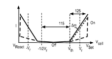
도 1b는, 실시예에 따른, 선택기 요소와 메모리 요소 사이에 장벽을 포함하는 박막 1S1R 비트셀의 I-V 응답을 나타내는 그래프이다;
도 2a는, 실시예에 따른, 선택기 유전체 재료와 메모리 산화물 재료 사이에 벌크 전도성 산화물 장벽 재료를 포함하는 박막 1S1R 비트셀의 단면도이다;
도 2b는, 실시예에 따른, 선택기 유전체 재료와 메모리 산화물 재료 사이에 금속 비산화물 화합물을 포함하는 박막 1S1R 비트셀의 단면도이다;
도 3a 및 도 3b는, 실시예들에 따른, 선택기 유전체 재료와 메모리 산화물 재료 사이에 다층 장벽을 포함하는 박막 1S1R 비트셀의 단면도이다;
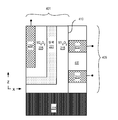
도 4는, 실시예들에 따른, 선택기 유전체 재료와 메모리 산화물 재료 사이에 전도성 산화물 장벽을 포함하는 비평면 박막 1S1R 비트셀을 나타내는 단면도이다;
도 5는 실시예들에 따른 적층된 박막 1S1R 비트셀을 나타내는 단면도이다;
도 6은, 실시예들에 따른, 선택기 산화물 재료와 메모리 산화물 재료 사이에 장벽을 포함하는 박막 1S1R 비트셀을 형성하는 방법을 나타내는 흐름도이다;
도 7은, 실시예들에 따른, 선택기 산화물 재료와 메모리 산화물 재료 사이에 다층 장벽을 포함하는 박막 1S1R 비트셀을 형성하는 방법을 나타내는 흐름도이다;
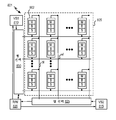
도 8은, 실시예들에 따른, 선택기 요소와 메모리 요소 사이에 장벽을 포함하는 복수의 박막 1S1R 비트셀을 포함하는 NVM의 개략도이다;
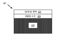
도 9은 실시예들에 따른 e-NVM의 단면을 나타낸다;
도 10은 본 발명의 실시예들에 따른 선택기 요소와 메모리 요소 사이에 장벽을 포함하는 1S1R 비트셀을 갖춘 e-NVM을 갖는 SoC를 채용하는 모바일 컴퓨팅 플랫폼 및 데이터 서버 머신을 나타낸다.
도 11은 본 발명의 실시예에 따른 전자 컴퓨팅 디바이스의 기능 블록도이다.
Claims (20)
- 저항식 메모리 셀로서,
기판;
상기 기판 위에 배치된 제1 및 제2 전극 재료;
상기 제1 전극 재료와 제2 전극 재료 사이에 배치된 박막 메모리 요소 및 박막 선택기 요소; 및
상기 메모리 요소와 상기 선택기 요소 사이에 배치된 전기적으로 부동상태의(electrically floating) 전도성 박막 장벽
을 포함하는 저항식 메모리 셀. - 제1항에 있어서,
상기 선택기 요소는, 임계 전압에서 저저항 상태와 고저항 상태 사이에서의 휘발성 천이를 겪는 제1 조성의 선택기 산화물 재료를 더 포함하고;
상기 메모리 요소는 셋/리셋 전압에서 저저항 상태와 고저항 상태 사이에서의 비휘발성 천이를 겪는 제2 조성의 메모리 산화물 재료를 더 포함하며;
상기 박막 장벽은, 벌크 전도성 금속 산화물 층, 또는 내화 금속(refractory metal) 질화물, 탄화물, 또는 탄질화물(carbonitride)을 포함하는 금속 비산화물 화합물 층(non-oxide metallic compound layer) 중 적어도 하나를 포함하는, 저항식 메모리 셀. - 제2항에 있어서, 상기 내화 금속 질화물, 탄화물, 또는 탄질화물은, TiN, TaN, WN, TiC, TaC, WC 또는 TaCN 중 적어도 하나를 포함하는, 저항식 메모리 셀.
- 제2항에 있어서, 상기 장벽은, RuO2, CrO2, WO2, IrO2, MoO2, PtO2, 또는 RhO2 중 적어도 하나를 포함하는 벌크 전도성 금속 산화물 층을 포함하는, 저항식 메모리 셀.
- 제2항에 있어서, 상기 장벽은, 상기 금속 비산화물 화합물 층, 및 상기 금속 비산화물 화합물 층과 상기 선택기 산화물 재료 및 상기 메모리 산화물 재료 중 적어도 하나 사이에 배치된 벌크 전도성 산화물 층을 포함하는 스택인, 저항식 메모리 셀.
- 제5항에 있어서,
상기 선택기 산화물 재료는 상기 메모리 산화물 재료 위에 배치되고, 상기 장벽은 상기 메모리 산화물 재료 위에 배치된 벌크 전도성 산화물 층을 포함하는 스택이고, 상기 금속 비산화물 화합물 층은 상기 벌크 전도성 산화물 층 위에 배치되거나, 또는
상기 메모리 산화물 재료는 상기 선택기 산화물 재료 위에 배치되고, 상기 장벽은 상기 선택기 산화물 재료 위에 배치된 벌크 전도성 산화물 층을 포함하는 스택이고, 상기 금속 비산화물 화합물 층은 상기 벌크 전도성 산화물 층 위에 배치되는, 저항식 메모리 셀. - 제2항에 있어서, 상기 장벽은 제1 벌크 전도성 금속 산화물 층과 제2 벌크 전도성 금속 산화물 층 사이에 배치된 금속 비산화물 화합물 층을 포함하는 스택인, 저항식 메모리 셀.
- 제7항에 있어서,
상기 금속 비산화물 화합물 층은, TiN, TaN, WN, TiC, TaC, WC 또는 TaCN 중 적어도 하나를 포함하고;
상기 제1 및 제2 벌크 전도성 금속 산화물 층은, RuO2, CrO2, WO2, IrO2, MoO2, PtO2, 또는 RhO2 중 적어도 하나를 포함하는, 저항식 메모리 셀. - 제1항에 있어서,
제1 및 제2 전극 재료 중 적어도 하나는, 벌크 전극 재료와 선택기 또는 메모리 요소 사이에 제2 박막 장벽을 포함하는 스택을 더 포함하는, 저항식 메모리 셀. - 제2항에 있어서,
상기 선택기 산화물 재료는 주로, 제1 산화 상태에서 천이 금속(transition metal)을 포함하고;
상기 선택기 산화물 재료는 주로, 상기 제1 산화 상태와는 상이한 제2 산화 상태에서 천이 금속을 포함하는, 저항식 메모리 셀. - 제2항에 있어서,
상기 선택기 산화물 재료는, VO2, Ta2O5, NbO2, Ti3O5, Ti2O3, LaCoO3 또는 SmNiO3 중 적어도 하나를 포함하고;
상기 메모리 산화물 재료는,
바나듐의 산화물, 크로뮴의 산화물, 니오븀의 산화물, 탄탈륨의 산화물, 및 하프늄(Hf)의 산화물로 구성된 그룹으로부터 선택된 음이온성-기반의 전도성 산화물 재료, 또는 LiMnO2, Li4TiO12, LiNiO2, LiNbO3 , Li3N:H, LiTiS2, Na b-알루미나, AgI, RbAg4I5, 및 AgGeAsS3으로 이루어진 그룹으로부터 선택된 양이온성-기반의 전도성 산화물 재료를 포함하는, 저항식 메모리 셀. - 시스템 온 칩(SoC; system on chip)으로서,
복수의 저항식 메모리 비트셀을 포함하는 저항식 메모리 어레이; 및
기판 위에 배치된 복수의 MOS 트랜지스터 ― 상기 복수의 트랜지스터 중 하나 이상은 상기 저항식 메모리 어레이에 전기적으로 결합됨 ―
를 포함하고,
각각의 비트셀은,
기판 위에 배치된 제1 및 제2 전극 재료;
상기 제1 전극 재료와 제2 전극 재료 사이에 배치된 박막 메모리 요소 및 박막 선택기 요소; 및
상기 메모리 요소와 선택기 요소 사이에 배치된 전기적으로 부동상태의 전도성 박막 장벽 ― 상기 제1 및 제2 전극 재료는 또한 워드 라인 및 비트 라인에 결합됨 ―
을 더 포함하는, SoC. - 저항식 메모리 셀을 제작하는 방법으로서,
기판 위에 제1 전극 재료를 퇴적하는 단계;
상기 제1 전극 재료 위에 박막 메모리 요소 및 박막 선택기 요소 중 하나를 퇴적하는 단계;
상기 메모리 또는 선택기 요소 위에 전도성 박막 장벽을 퇴적하는 단계;
상기 장벽 위에 상기 메모리 요소 및 상기 선택기 요소 중 다른 하나를 퇴적하는 단계; 및
상기 메모리 요소 및 상기 선택기 요소 중 상기 다른 하나 위에 제2 전극 재료를 퇴적하는 단계
를 포함하는 방법. - 제13항에 있어서,
상기 메모리 요소를 퇴적하는 단계는, 셋/리셋 전압에서 저저항 상태와 고저항 상태 사이에서의 비휘발성 천이를 겪는 제1 조성의 메모리 산화물을 퇴적하는 단계를 더 포함하고;
상기 선택기 요소를 퇴적하는 단계는, 임계 전압에서 저저항 상태와 고저항 상태 사이에서의 휘발성 천이를 겪는 제2 조성의 선택기 산화물 재료를 퇴적하는 단계를 더 포함하며;
상기 장벽을 퇴적하는 단계는, 내화 금속의 질화물, 탄화물, 또는 탄질화물을 포함하는 금속 비산화물 화합물 층을 퇴적하는 단계를 더 포함하는, 방법. - 제14항에 있어서, 상기 금속 비산화물 화합물 층을 퇴적하는 단계는, TiN, TaN, WN, TiC, TaC, WC 및 TaCN 중 적어도 하나를 퇴적하는 단계를 더 포함하는, 방법.
- 제13항에 있어서, 상기 장벽을 퇴적하는 단계는,
상기 선택기 요소의 메모리 위에 벌크 전도성 산화물을 퇴적하는 단계, 및
상기 벌크 전도성 산화물 위에 금속 비산화물 화합물 층을 퇴적하는 단계
를 더 포함하는, 방법. - 제16항에 있어서, 상기 벌크 전도성 산화물을 퇴적하는 단계는, RuO2, CrO2, WO2, IrO2, MoO2, PtO2 또는 RhO2 중 적어도 하나를 퇴적하는 단계를 더 포함하는, 방법.
- 제16항에 있어서, 상기 장벽을 퇴적하는 단계는, 상기 금속 비산화물 화합물 층 위에 제2 벌크 전도성 산화물 층을 퇴적하는 단계를 더 포함하는, 방법.
- 제13항에 있어서,
상기 메모리 산화물 재료 및 선택기 산화물 재료 중 적어도 하나를 퇴적하는 단계는, 원자 층 퇴적(ALD) 프로세스로 지형 피쳐(topographic feature)의 측벽 상에 상기 산화물 재료를 퇴적하는 단계를 더 포함하고;
상기 장벽을 퇴적하는 단계는 ALD 프로세스로 금속 비산화물 화합물을 퇴적하는 단계를 더 포함하는, 방법. - 제13항에 있어서, 상기 선택기 요소를 퇴적하는 단계는, VO2, Ta2O5, NbO2, Ti3O5, Ti2O3, LaCoO3 또는 SmNiO3를 퇴적하는 단계를 더 포함하는, 방법.
Applications Claiming Priority (1)
| Application Number | Priority Date | Filing Date | Title |
|---|---|---|---|
| PCT/US2014/057494 WO2016048330A1 (en) | 2014-09-25 | 2014-09-25 | 1s1r memory cells incorporating a barrier layer |
Publications (2)
| Publication Number | Publication Date |
|---|---|
| KR20170059971A true KR20170059971A (ko) | 2017-05-31 |
| KR102244116B1 KR102244116B1 (ko) | 2021-04-26 |
Family
ID=55581650
Family Applications (1)
| Application Number | Title | Priority Date | Filing Date |
|---|---|---|---|
| KR1020177004308A Active KR102244116B1 (ko) | 2014-09-25 | 2014-09-25 | 장벽 층을 포함하는 1s1r 메모리 셀 |
Country Status (7)
| Country | Link |
|---|---|
| US (1) | US20170288140A1 (ko) |
| EP (1) | EP3198645A4 (ko) |
| JP (1) | JP6628108B2 (ko) |
| KR (1) | KR102244116B1 (ko) |
| CN (1) | CN106663683B (ko) |
| TW (1) | TW201624676A (ko) |
| WO (1) | WO2016048330A1 (ko) |
Cited By (4)
| Publication number | Priority date | Publication date | Assignee | Title |
|---|---|---|---|---|
| US10355205B2 (en) | 2014-12-18 | 2019-07-16 | Intel Corporation | Resistive memory cells including localized filamentary channels, devices including the same, and methods of making the same |
| KR20190123976A (ko) | 2018-04-25 | 2019-11-04 | 포항공과대학교 산학협력단 | 스위치 역할을 하는 선택소자가 포함된 저항변화 메모리 |
| US10516109B2 (en) | 2014-12-24 | 2019-12-24 | Intel Corporation | Resistive memory cells and precursors thereof, methods of making the same, and devices including the same |
| KR20210084194A (ko) * | 2019-12-26 | 2021-07-07 | 타이완 세미콘덕터 매뉴팩쳐링 컴퍼니 리미티드 | 라인형 메모리 및 그 형성 방법 |
Families Citing this family (18)
| Publication number | Priority date | Publication date | Assignee | Title |
|---|---|---|---|---|
| US10910436B2 (en) | 2016-09-24 | 2021-02-02 | Intel Corporation | Asymmetric selectors for memory cells |
| US20200058704A1 (en) * | 2017-02-22 | 2020-02-20 | Institute of Microelectronics, Chinese Academy of Sciences | Selector based on transition metal oxide and preparation method therefor |
| US10114590B1 (en) * | 2017-05-31 | 2018-10-30 | Sandisk Technologies Llc | Methods for three-dimensional nonvolatile memory that include multi-portion word lines |
| US10340449B2 (en) * | 2017-06-01 | 2019-07-02 | Sandisk Technologies Llc | Resistive memory device containing carbon barrier and method of making thereof |
| KR20180134123A (ko) * | 2017-06-08 | 2018-12-18 | 에스케이하이닉스 주식회사 | 저항 변화 메모리 소자 |
| US11233090B2 (en) | 2017-09-27 | 2022-01-25 | Intel Corporation | Double selector element for low voltage bipolar memory devices |
| WO2019218106A1 (zh) * | 2018-05-14 | 2019-11-21 | 中国科学院微电子研究所 | 1s1r存储器集成结构及其制备方法 |
| CN109036486B (zh) * | 2018-07-03 | 2022-02-25 | 中国科学院微电子研究所 | 存储器件的读取方法 |
| US11404639B2 (en) * | 2018-08-28 | 2022-08-02 | Intel Corporation | Selector devices with integrated barrier materials |
| JP2020150082A (ja) * | 2019-03-12 | 2020-09-17 | キオクシア株式会社 | 記憶装置 |
| US10950788B1 (en) * | 2019-08-20 | 2021-03-16 | 4DS Memory, Limited | Resistive memory device having an oxide barrier layer |
| US11133464B2 (en) | 2019-08-20 | 2021-09-28 | 4DS Memory, Limited | Conductive amorphous oxide contact layers |
| US11659778B2 (en) * | 2020-02-11 | 2023-05-23 | Micron Technology, Inc. | Composite electrode material chemistry |
| CN111933794B (zh) * | 2020-07-02 | 2023-08-01 | 北京航空航天大学 | 基于模拟型和数字型共存的MoS2基忆阻器及其制备方法 |
| US12256557B2 (en) | 2022-01-19 | 2025-03-18 | SanDisk Technologies, Inc. | Ovonic threshold switch selectors with electrodes including carbon and metal |
| CN115241371B (zh) * | 2022-08-04 | 2026-04-24 | 复旦大学 | 一种具有选通与多比特存储功能的阵列集成器件及其制备方法 |
| CN116075212B (zh) * | 2023-03-06 | 2023-07-14 | 昕原半导体(上海)有限公司 | 电阻式随机存取存储器及其制备方法 |
| CN119384214B (zh) * | 2024-09-30 | 2025-11-04 | 北京大学 | 基于1s1r结构的自选择存储器及其制备方法、设备 |
Citations (4)
| Publication number | Priority date | Publication date | Assignee | Title |
|---|---|---|---|---|
| KR20120136963A (ko) * | 2011-06-10 | 2012-12-20 | 서울대학교산학협력단 | 3차원 비휘발성 메모리 장치 및 이의 제조 방법 |
| US20140008602A1 (en) * | 2012-07-06 | 2014-01-09 | Micron Technology, Inc. | Thermal isolation in memory cells |
| WO2014036264A1 (en) * | 2012-08-30 | 2014-03-06 | Micron Technology, Inc. | Resistive memory devices |
| US20140246643A1 (en) * | 2013-03-04 | 2014-09-04 | Samsung Electronics Co., Ltd. | Memory device and apparatus including the same |
Family Cites Families (10)
| Publication number | Priority date | Publication date | Assignee | Title |
|---|---|---|---|---|
| JP5364407B2 (ja) * | 2009-03-24 | 2013-12-11 | 株式会社東芝 | 不揮発性記憶装置及びその製造方法 |
| WO2011096940A1 (en) * | 2010-02-08 | 2011-08-11 | Hewlett-Packard Development Company, L.P. | Memory resistor having multi-layer electrodes |
| KR20130004784A (ko) * | 2011-07-04 | 2013-01-14 | 삼성전자주식회사 | 저항 변화 체를 갖는 비-휘발성 메모리 소자 및 그 제조방법 |
| US9847478B2 (en) * | 2012-03-09 | 2017-12-19 | Taiwan Semiconductor Manufacturing Company, Ltd. | Methods and apparatus for resistive random access memory (RRAM) |
| JP5606478B2 (ja) * | 2012-03-22 | 2014-10-15 | 株式会社東芝 | 半導体記憶装置 |
| US8729523B2 (en) * | 2012-08-31 | 2014-05-20 | Micron Technology, Inc. | Three dimensional memory array architecture |
| CN102903845B (zh) * | 2012-09-10 | 2015-05-13 | 北京大学 | 一种阻变存储器及其制备方法 |
| EP2814073B1 (en) * | 2013-06-14 | 2017-02-15 | IMEC vzw | Self-rectifying RRAM element |
| US9911788B2 (en) * | 2014-05-05 | 2018-03-06 | Hewlett Packard Enterprise Development Lp | Selectors with oxide-based layers |
| WO2015199692A1 (en) * | 2014-06-26 | 2015-12-30 | Hewlett-Packard Development Company, L.P. | Protective elements for non-volatile memory cells in crossbar arrays |
-
2014
- 2014-09-25 KR KR1020177004308A patent/KR102244116B1/ko active Active
- 2014-09-25 US US15/505,909 patent/US20170288140A1/en not_active Abandoned
- 2014-09-25 WO PCT/US2014/057494 patent/WO2016048330A1/en not_active Ceased
- 2014-09-25 JP JP2017509005A patent/JP6628108B2/ja active Active
- 2014-09-25 EP EP14902489.5A patent/EP3198645A4/en not_active Withdrawn
- 2014-09-25 CN CN201480081430.9A patent/CN106663683B/zh not_active Expired - Fee Related
-
2015
- 2015-08-19 TW TW104127004A patent/TW201624676A/zh unknown
Patent Citations (5)
| Publication number | Priority date | Publication date | Assignee | Title |
|---|---|---|---|---|
| KR20120136963A (ko) * | 2011-06-10 | 2012-12-20 | 서울대학교산학협력단 | 3차원 비휘발성 메모리 장치 및 이의 제조 방법 |
| US20140008602A1 (en) * | 2012-07-06 | 2014-01-09 | Micron Technology, Inc. | Thermal isolation in memory cells |
| WO2014036264A1 (en) * | 2012-08-30 | 2014-03-06 | Micron Technology, Inc. | Resistive memory devices |
| US20140061568A1 (en) * | 2012-08-30 | 2014-03-06 | Durai Vishak Nirmal Ramaswamy | Resistive memory devices |
| US20140246643A1 (en) * | 2013-03-04 | 2014-09-04 | Samsung Electronics Co., Ltd. | Memory device and apparatus including the same |
Cited By (5)
| Publication number | Priority date | Publication date | Assignee | Title |
|---|---|---|---|---|
| US10355205B2 (en) | 2014-12-18 | 2019-07-16 | Intel Corporation | Resistive memory cells including localized filamentary channels, devices including the same, and methods of making the same |
| US10516109B2 (en) | 2014-12-24 | 2019-12-24 | Intel Corporation | Resistive memory cells and precursors thereof, methods of making the same, and devices including the same |
| KR20190123976A (ko) | 2018-04-25 | 2019-11-04 | 포항공과대학교 산학협력단 | 스위치 역할을 하는 선택소자가 포함된 저항변화 메모리 |
| KR20210084194A (ko) * | 2019-12-26 | 2021-07-07 | 타이완 세미콘덕터 매뉴팩쳐링 컴퍼니 리미티드 | 라인형 메모리 및 그 형성 방법 |
| US11404480B2 (en) | 2019-12-26 | 2022-08-02 | Taiwan Semiconductor Manufacturing Company, Ltd. | Memory arrays including continuous line-shaped random access memory strips and method forming same |
Also Published As
| Publication number | Publication date |
|---|---|
| JP2017532765A (ja) | 2017-11-02 |
| KR102244116B1 (ko) | 2021-04-26 |
| US20170288140A1 (en) | 2017-10-05 |
| CN106663683A (zh) | 2017-05-10 |
| WO2016048330A1 (en) | 2016-03-31 |
| CN106663683B (zh) | 2021-02-09 |
| TW201624676A (zh) | 2016-07-01 |
| EP3198645A4 (en) | 2018-05-23 |
| EP3198645A1 (en) | 2017-08-02 |
| JP6628108B2 (ja) | 2020-01-08 |
Similar Documents
| Publication | Publication Date | Title |
|---|---|---|
| KR102244116B1 (ko) | 장벽 층을 포함하는 1s1r 메모리 셀 | |
| JP6642839B2 (ja) | 抵抗変化型ランダムアクセスメモリセルにおける酸化物メモリエレメントを接続する希土類金属及び金属酸化物電極 | |
| US8759806B2 (en) | Semiconductor memory device | |
| US8507887B2 (en) | Resistance change memory and method of manufacturing the same | |
| CN106062879B (zh) | 切换组件及存储器单元 | |
| US20140097397A1 (en) | Resistive memory device and memory apparatus and data processing system having the same | |
| US8937830B2 (en) | Semiconductor memory device | |
| JP5291269B2 (ja) | 不揮発性半導体記憶素子、不揮発性半導体記憶装置およびその製造方法 | |
| US20130128654A1 (en) | Nonvolatile memory element, method of manufacturing nonvolatile memory element, method of initial breakdown of nonvolatile memory element, and nonvolatile memory device | |
| US20130235646A1 (en) | Semiconductor memory device | |
| US9105332B2 (en) | Variable resistance nonvolatile memory device | |
| KR20140081135A (ko) | 다층 터널 배리어 선택 소자를 이용한 비선형 저항 스위칭 메모리 소자 및 그 제조방법 |
Legal Events
| Date | Code | Title | Description |
|---|---|---|---|
| PA0105 | International application |
Patent event date: 20170216 Patent event code: PA01051R01D Comment text: International Patent Application |
|
| PG1501 | Laying open of application | ||
| A201 | Request for examination | ||
| PA0201 | Request for examination |
Patent event code: PA02012R01D Patent event date: 20190925 Comment text: Request for Examination of Application |
|
| E902 | Notification of reason for refusal | ||
| PE0902 | Notice of grounds for rejection |
Comment text: Notification of reason for refusal Patent event date: 20200820 Patent event code: PE09021S01D |
|
| E701 | Decision to grant or registration of patent right | ||
| PE0701 | Decision of registration |
Patent event code: PE07011S01D Comment text: Decision to Grant Registration Patent event date: 20210223 |
|
| GRNT | Written decision to grant | ||
| PR0701 | Registration of establishment |
Comment text: Registration of Establishment Patent event date: 20210419 Patent event code: PR07011E01D |
|
| PR1002 | Payment of registration fee |
Payment date: 20210420 End annual number: 3 Start annual number: 1 |
|
| PG1601 | Publication of registration | ||
| PR1001 | Payment of annual fee |
Payment date: 20231205 Start annual number: 4 End annual number: 4 |
|
| PR1001 | Payment of annual fee |
Payment date: 20241128 Start annual number: 5 End annual number: 5 |