KR20170061069A - 애퍼쳐의 얼라인먼트 방법 및 멀티 하전 입자 빔 묘화 장치 - Google Patents
애퍼쳐의 얼라인먼트 방법 및 멀티 하전 입자 빔 묘화 장치 Download PDFInfo
- Publication number
- KR20170061069A KR20170061069A KR1020160154114A KR20160154114A KR20170061069A KR 20170061069 A KR20170061069 A KR 20170061069A KR 1020160154114 A KR1020160154114 A KR 1020160154114A KR 20160154114 A KR20160154114 A KR 20160154114A KR 20170061069 A KR20170061069 A KR 20170061069A
- Authority
- KR
- South Korea
- Prior art keywords
- aperture
- current
- charged particle
- amount
- particle beam
- Prior art date
- Legal status (The legal status is an assumption and is not a legal conclusion. Google has not performed a legal analysis and makes no representation as to the accuracy of the status listed.)
- Granted
Links
- 239000002245 particle Substances 0.000 title claims abstract description 32
- 238000000034 method Methods 0.000 title claims abstract description 16
- 238000000465 moulding Methods 0.000 claims abstract description 61
- 238000009826 distribution Methods 0.000 claims abstract description 55
- 238000007493 shaping process Methods 0.000 claims abstract description 13
- 230000001678 irradiating effect Effects 0.000 claims abstract description 5
- NJPPVKZQTLUDBO-UHFFFAOYSA-N novaluron Chemical compound C1=C(Cl)C(OC(F)(F)C(OC(F)(F)F)F)=CC=C1NC(=O)NC(=O)C1=C(F)C=CC=C1F NJPPVKZQTLUDBO-UHFFFAOYSA-N 0.000 claims description 14
- 238000003384 imaging method Methods 0.000 claims description 7
- 238000007599 discharging Methods 0.000 claims description 3
- 238000010894 electron beam technology Methods 0.000 description 53
- 238000010586 diagram Methods 0.000 description 11
- 239000011295 pitch Substances 0.000 description 6
- 239000004065 semiconductor Substances 0.000 description 5
- 238000005286 illumination Methods 0.000 description 3
- 239000000470 constituent Substances 0.000 description 2
- VYPSYNLAJGMNEJ-UHFFFAOYSA-N silicon dioxide Inorganic materials O=[Si]=O VYPSYNLAJGMNEJ-UHFFFAOYSA-N 0.000 description 2
- 239000000758 substrate Substances 0.000 description 2
- XUIMIQQOPSSXEZ-UHFFFAOYSA-N Silicon Chemical compound [Si] XUIMIQQOPSSXEZ-UHFFFAOYSA-N 0.000 description 1
- 238000006073 displacement reaction Methods 0.000 description 1
- 238000000609 electron-beam lithography Methods 0.000 description 1
- 238000005516 engineering process Methods 0.000 description 1
- 230000010354 integration Effects 0.000 description 1
- 238000010884 ion-beam technique Methods 0.000 description 1
- 238000004519 manufacturing process Methods 0.000 description 1
- 239000010453 quartz Substances 0.000 description 1
- 229910052710 silicon Inorganic materials 0.000 description 1
- 239000010703 silicon Substances 0.000 description 1
Images


Classifications
-
- G—PHYSICS
- G03—PHOTOGRAPHY; CINEMATOGRAPHY; ANALOGOUS TECHNIQUES USING WAVES OTHER THAN OPTICAL WAVES; ELECTROGRAPHY; HOLOGRAPHY
- G03F—PHOTOMECHANICAL PRODUCTION OF TEXTURED OR PATTERNED SURFACES, e.g. FOR PRINTING, FOR PROCESSING OF SEMICONDUCTOR DEVICES; MATERIALS THEREFOR; ORIGINALS THEREFOR; APPARATUS SPECIALLY ADAPTED THEREFOR
- G03F7/00—Photomechanical, e.g. photolithographic, production of textured or patterned surfaces, e.g. printing surfaces; Materials therefor, e.g. comprising photoresists; Apparatus specially adapted therefor
- G03F7/20—Exposure; Apparatus therefor
- G03F7/2051—Exposure without an original mask, e.g. using a programmed deflection of a point source, by scanning, by drawing with a light beam, using an addressed light or corpuscular source
- G03F7/2059—Exposure without an original mask, e.g. using a programmed deflection of a point source, by scanning, by drawing with a light beam, using an addressed light or corpuscular source using a scanning corpuscular radiation beam, e.g. an electron beam
-
- G—PHYSICS
- G03—PHOTOGRAPHY; CINEMATOGRAPHY; ANALOGOUS TECHNIQUES USING WAVES OTHER THAN OPTICAL WAVES; ELECTROGRAPHY; HOLOGRAPHY
- G03F—PHOTOMECHANICAL PRODUCTION OF TEXTURED OR PATTERNED SURFACES, e.g. FOR PRINTING, FOR PROCESSING OF SEMICONDUCTOR DEVICES; MATERIALS THEREFOR; ORIGINALS THEREFOR; APPARATUS SPECIALLY ADAPTED THEREFOR
- G03F7/00—Photomechanical, e.g. photolithographic, production of textured or patterned surfaces, e.g. printing surfaces; Materials therefor, e.g. comprising photoresists; Apparatus specially adapted therefor
- G03F7/70—Microphotolithographic exposure; Apparatus therefor
- G03F7/70691—Handling of masks or workpieces
- G03F7/70775—Position control, e.g. interferometers or encoders for determining the stage position
-
- G—PHYSICS
- G03—PHOTOGRAPHY; CINEMATOGRAPHY; ANALOGOUS TECHNIQUES USING WAVES OTHER THAN OPTICAL WAVES; ELECTROGRAPHY; HOLOGRAPHY
- G03F—PHOTOMECHANICAL PRODUCTION OF TEXTURED OR PATTERNED SURFACES, e.g. FOR PRINTING, FOR PROCESSING OF SEMICONDUCTOR DEVICES; MATERIALS THEREFOR; ORIGINALS THEREFOR; APPARATUS SPECIALLY ADAPTED THEREFOR
- G03F1/00—Originals for photomechanical production of textured or patterned surfaces, e.g., masks, photo-masks, reticles; Mask blanks or pellicles therefor; Containers specially adapted therefor; Preparation thereof
- G03F1/20—Masks or mask blanks for imaging by charged particle beam [CPB] radiation, e.g. by electron beam; Preparation thereof
-
- G—PHYSICS
- G03—PHOTOGRAPHY; CINEMATOGRAPHY; ANALOGOUS TECHNIQUES USING WAVES OTHER THAN OPTICAL WAVES; ELECTROGRAPHY; HOLOGRAPHY
- G03F—PHOTOMECHANICAL PRODUCTION OF TEXTURED OR PATTERNED SURFACES, e.g. FOR PRINTING, FOR PROCESSING OF SEMICONDUCTOR DEVICES; MATERIALS THEREFOR; ORIGINALS THEREFOR; APPARATUS SPECIALLY ADAPTED THEREFOR
- G03F1/00—Originals for photomechanical production of textured or patterned surfaces, e.g., masks, photo-masks, reticles; Mask blanks or pellicles therefor; Containers specially adapted therefor; Preparation thereof
- G03F1/38—Masks having auxiliary features, e.g. special coatings or marks for alignment or testing; Preparation thereof
- G03F1/42—Alignment or registration features, e.g. alignment marks on the mask substrates
-
- G—PHYSICS
- G03—PHOTOGRAPHY; CINEMATOGRAPHY; ANALOGOUS TECHNIQUES USING WAVES OTHER THAN OPTICAL WAVES; ELECTROGRAPHY; HOLOGRAPHY
- G03F—PHOTOMECHANICAL PRODUCTION OF TEXTURED OR PATTERNED SURFACES, e.g. FOR PRINTING, FOR PROCESSING OF SEMICONDUCTOR DEVICES; MATERIALS THEREFOR; ORIGINALS THEREFOR; APPARATUS SPECIALLY ADAPTED THEREFOR
- G03F7/00—Photomechanical, e.g. photolithographic, production of textured or patterned surfaces, e.g. printing surfaces; Materials therefor, e.g. comprising photoresists; Apparatus specially adapted therefor
- G03F7/70—Microphotolithographic exposure; Apparatus therefor
- G03F7/70216—Mask projection systems
- G03F7/7025—Size or form of projection system aperture, e.g. aperture stops, diaphragms or pupil obscuration; Control thereof
-
- G—PHYSICS
- G03—PHOTOGRAPHY; CINEMATOGRAPHY; ANALOGOUS TECHNIQUES USING WAVES OTHER THAN OPTICAL WAVES; ELECTROGRAPHY; HOLOGRAPHY
- G03F—PHOTOMECHANICAL PRODUCTION OF TEXTURED OR PATTERNED SURFACES, e.g. FOR PRINTING, FOR PROCESSING OF SEMICONDUCTOR DEVICES; MATERIALS THEREFOR; ORIGINALS THEREFOR; APPARATUS SPECIALLY ADAPTED THEREFOR
- G03F7/00—Photomechanical, e.g. photolithographic, production of textured or patterned surfaces, e.g. printing surfaces; Materials therefor, e.g. comprising photoresists; Apparatus specially adapted therefor
- G03F7/70—Microphotolithographic exposure; Apparatus therefor
- G03F7/708—Construction of apparatus, e.g. environment aspects, hygiene aspects or materials
- G03F7/7085—Detection arrangement, e.g. detectors of apparatus alignment possibly mounted on wafers, exposure dose, photo-cleaning flux, stray light, thermal load
-
- G—PHYSICS
- G03—PHOTOGRAPHY; CINEMATOGRAPHY; ANALOGOUS TECHNIQUES USING WAVES OTHER THAN OPTICAL WAVES; ELECTROGRAPHY; HOLOGRAPHY
- G03F—PHOTOMECHANICAL PRODUCTION OF TEXTURED OR PATTERNED SURFACES, e.g. FOR PRINTING, FOR PROCESSING OF SEMICONDUCTOR DEVICES; MATERIALS THEREFOR; ORIGINALS THEREFOR; APPARATUS SPECIALLY ADAPTED THEREFOR
- G03F9/00—Registration or positioning of originals, masks, frames, photographic sheets or textured or patterned surfaces, e.g. automatically
- G03F9/70—Registration or positioning of originals, masks, frames, photographic sheets or textured or patterned surfaces, e.g. automatically for microlithography
- G03F9/7003—Alignment type or strategy, e.g. leveling, global alignment
-
- H—ELECTRICITY
- H01—ELECTRIC ELEMENTS
- H01J—ELECTRIC DISCHARGE TUBES OR DISCHARGE LAMPS
- H01J37/00—Discharge tubes with provision for introducing objects or material to be exposed to the discharge, e.g. for the purpose of examination or processing thereof
- H01J37/30—Electron-beam or ion-beam tubes for localised treatment of objects
- H01J37/304—Controlling tubes by information coming from the objects or from the beam, e.g. correction signals
- H01J37/3045—Object or beam position registration
-
- H—ELECTRICITY
- H01—ELECTRIC ELEMENTS
- H01J—ELECTRIC DISCHARGE TUBES OR DISCHARGE LAMPS
- H01J37/00—Discharge tubes with provision for introducing objects or material to be exposed to the discharge, e.g. for the purpose of examination or processing thereof
- H01J37/30—Electron-beam or ion-beam tubes for localised treatment of objects
- H01J37/317—Electron-beam or ion-beam tubes for localised treatment of objects for changing properties of the objects or for applying thin layers thereon, e.g. for ion implantation
- H01J37/3174—Particle-beam lithography, e.g. electron beam lithography
- H01J37/3177—Multi-beam, e.g. fly's eye, comb probe
-
- H—ELECTRICITY
- H01—ELECTRIC ELEMENTS
- H01J—ELECTRIC DISCHARGE TUBES OR DISCHARGE LAMPS
- H01J2237/00—Discharge tubes exposing object to beam, e.g. for analysis treatment, etching, imaging
- H01J2237/04—Means for controlling the discharge
- H01J2237/043—Beam blanking
- H01J2237/0435—Multi-aperture
-
- H—ELECTRICITY
- H01—ELECTRIC ELEMENTS
- H01J—ELECTRIC DISCHARGE TUBES OR DISCHARGE LAMPS
- H01J2237/00—Discharge tubes exposing object to beam, e.g. for analysis treatment, etching, imaging
- H01J2237/04—Means for controlling the discharge
- H01J2237/045—Diaphragms
- H01J2237/0456—Supports
- H01J2237/0458—Supports movable, i.e. for changing between differently sized apertures
-
- H—ELECTRICITY
- H01—ELECTRIC ELEMENTS
- H01J—ELECTRIC DISCHARGE TUBES OR DISCHARGE LAMPS
- H01J2237/00—Discharge tubes exposing object to beam, e.g. for analysis treatment, etching, imaging
- H01J2237/15—Means for deflecting or directing discharge
- H01J2237/1501—Beam alignment means or procedures
Landscapes
- Physics & Mathematics (AREA)
- General Physics & Mathematics (AREA)
- Chemical & Material Sciences (AREA)
- Analytical Chemistry (AREA)
- Health & Medical Sciences (AREA)
- Toxicology (AREA)
- Engineering & Computer Science (AREA)
- Environmental & Geological Engineering (AREA)
- Epidemiology (AREA)
- Public Health (AREA)
- Electron Sources, Ion Sources (AREA)
- Electron Beam Exposure (AREA)
Abstract
Description
도 2는, 애퍼쳐 스테이지의 개략도이다.
도 3의 (a)는, 성형 애퍼쳐의 개략도이고, 도 3의 (b)는 블랭킹 애퍼쳐의 개략도이다.
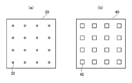
도 4의 (a), 도 4의 (b)는 애퍼쳐의 위치 어긋남 예를 나타내는 도면이다.
도 5의 (a)는, 빔이 블랭킹 애퍼쳐를 통과하지 않는 예를 도시하는 도면이고, 도 5의 (b)는 편향된 빔이 블랭킹 애퍼쳐를 통과하는 예를 도시하는 도면이다.
도 6은, 전류량 분포 맵의 작성 방법을 도시하는 도면이다.
도 7은, 전류량 분포 맵의 예를 도시하는 도면이다.
도 8의 (a)는, 애퍼쳐의 위치 어긋남 예를 나타내는 도면이고, 도 8의 (b)는 전류량 분포 맵의 예를 도시하는 도면이다.
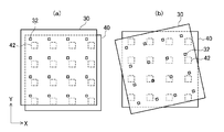
도 9의 (a)는, 애퍼쳐의 위치 어긋남 예를 나타내는 도면이고, 도 9의 (b)는 전류량 분포 맵의 예를 도시하는 도면이다.
도 10의 (a), 도 10의 (b)는 블랭킹 애퍼쳐를 통과하는 빔과 통과하지 않은 빔을 도시하는 도면이고, 도 10의 (c)는 전류량 분포 맵의 예를 도시하는 도면이다.
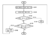
도 11은, 본 실시 형태에 따른 애퍼쳐의 얼라인먼트 방법을 설명하는 흐름도이다.
도 12의 (a), 도 12의 (b)는 빔의 편향 영역과, 블랭킹 애퍼쳐의 통과 구멍의 개구 피치를 도시하는 도면이다.
Claims (10)
- 하전 입자 빔을 방출하는 방출부와,
상기 하전 입자 빔의 조사를 받아서 멀티 빔을 형성하는 복수의 제1 개구부가 형성된 성형 애퍼쳐와,
상기 복수의 제1 개구부에 대응한 제2 개구부가 형성되고, 각 제2 개구부에, 상기 멀티 빔 중, 각각 대응하는 빔에 대하여 블랭킹 편향을 행하는 블랭커가 배치된 블랭킹 애퍼쳐와,
상기 방출부에서 방출된 하전 입자 빔을 편향하고, 상기 성형 애퍼쳐에의 상기 하전 입자 빔의 입사 방향을 변화시키는 입사 방향 제어부와,
상기 블랭킹 애퍼쳐를 통과한 멀티 빔의 전류량을 검출하는 검출기
를 구비하는 멀티 하전 입자 빔 묘화 장치의 애퍼쳐의 얼라인먼트 방법이며,
상기 입사 방향 제어부에 의해 상기 입사 방향을 변화시키면서, 상기 하전 입자 빔을 상기 성형 애퍼쳐에 조사하는 공정과,
상기 검출기를 사용하여, 상기 하전 입자 빔의 입사 방향마다, 상기 전류량을 검출하는 공정과,
상기 입사 방향과 상기 전류량에 기초하여 전류량 분포 맵을 작성하는 공정과,
상기 전류량 분포 맵에 기초하여 상기 성형 애퍼쳐 또는 상기 블랭킹 애퍼쳐를 이동시켜, 상기 성형 애퍼쳐와 상기 블랭킹 애퍼쳐와의 위치 정렬을 행하는 공정
을 구비하는 것을 특징으로 하는 애퍼쳐의 얼라인먼트 방법. - 제1항에 있어서, 상기 전류량 분포 맵은 입사 방향에 기초하는 위치의 휘도를 전류량에 따른 것으로 한 휘도 분포 화상이고,
상기 전류량 분포 맵에 있어서의 고전류 영역의 위치에 기초하여, 상기 성형 애퍼쳐 또는 상기 블랭킹 애퍼쳐의 이동량을 결정하는 것을 특징으로 하는 애퍼쳐의 얼라인먼트 방법. - 제1항에 있어서, 입사 방향마다의 전류량의 차가 소정 값 이하인 경우, 상기 성형 애퍼쳐 또는 상기 블랭킹 애퍼쳐를 회전시키는 것을 특징으로 하는 애퍼쳐의 얼라인먼트 방법.
- 제1항에 있어서, 상기 입사 방향 제어부에 의한 상기 블랭킹 애퍼쳐 상에서의 빔의 최대 편향량이, 상기 제2 개구부의 개구 피치 이상인 것을 특징으로 하는 애퍼쳐의 얼라인먼트 방법.
- 하전 입자 빔을 방출하는 방출부와,
상기 하전 입자 빔의 조사를 받아서 멀티 빔을 형성하는 복수의 제1 개구부가 형성된 성형 애퍼쳐와,
상기 복수의 제1 개구부에 대응한 제2 개구부가 형성되고, 각 제2 개구부에, 상기 멀티 빔 중, 각각 대응하는 빔에 대하여 블랭킹 편향을 행하는 블랭커가 배치된 블랭킹 애퍼쳐와,
상기 방출부에서 방출된 하전 입자 빔을 편향하고, 상기 성형 애퍼쳐에의 상기 하전 입자 빔의 입사 방향을 변화시키는 얼라인먼트 코일과,
상기 블랭킹 애퍼쳐를 통과한 멀티 빔의 전류량을 검출하는 검출기와,
상기 얼라인먼트 코일에 의해 상기 입사 방향을 변화시키면서, 상기 하전 입자 빔을 상기 성형 애퍼쳐에 조사시켜, 상기 입사 방향과, 입사 방향마다 상기 검출기가 검출한 전류량에 기초하여 전류량 분포 맵을 작성하고, 상기 전류량 분포 맵에 기초하여 상기 성형 애퍼쳐 또는 상기 블랭킹 애퍼쳐를 이동시켜, 상기 성형 애퍼쳐와 상기 블랭킹 애퍼쳐와의 위치 정렬을 행하는 제어부
를 구비하는 멀티 하전 입자 빔 묘화 장치. - 제5항에 있어서, 상기 전류량 분포 맵은, 입사 방향에 기초하는 위치의 휘도를 전류량에 따른 것으로 한 휘도 분포 화상이고,
상기 제어부는, 상기 전류량 분포 맵에 있어서의 고전류 영역의 위치에 기초하여, 상기 성형 애퍼쳐 또는 상기 블랭킹 애퍼쳐의 이동량을 결정하는 것을 특징으로 하는 멀티 하전 입자 빔 묘화 장치. - 제5항에 있어서, 상기 제어부는, 입사 방향마다의 전류량의 차가 소정 값 이하인 경우, 상기 성형 애퍼쳐 또는 상기 블랭킹 애퍼쳐를 회전시키는 것을 특징으로 하는 멀티 하전 입자 빔 묘화 장치.
- 제5항에 있어서, 상기 얼라인먼트 코일에 의한 상기 블랭킹 애퍼쳐 상에서의 빔의 최대 편향량은, 상기 제2 개구부의 개구 피치 이상인 것을 특징으로 하는 멀티 하전 입자 빔 묘화 장치.
- 제8항에 있어서, 상기 제어부는, 상기 검출기가 모든 빔을 차폐했을 때에 검출한 전류량에 기초하여, 상기 전류량 분포 맵을 작성하는 것을 특징으로 하는 멀티 하전 입자 빔 묘화 장치.
- 제5항에 있어서, 제1 받침대와,
상기 제1 받침대의 주연부로부터 세워서 설치하는 이동 가능한 복수의 제1 지주와,
상기 제1 지주의 상방에 설치되어, 상기 성형 애퍼쳐가 적재되는 제2 받침대와,
상기 제1 받침대의 상기 제1 지주보다 내주측에서 세워서 설치하는 복수의 제2 지주와,
상기 제2 지주의 상방에 설치되어, 상기 블랭킹 애퍼쳐가 적재되는 제3 받침대
를 더 구비하는 것을 특징으로 하는 멀티 하전 입자 빔 묘화 장치.
Applications Claiming Priority (2)
| Application Number | Priority Date | Filing Date | Title |
|---|---|---|---|
| JPJP-P-2015-229833 | 2015-11-25 | ||
| JP2015229833A JP6589597B2 (ja) | 2015-11-25 | 2015-11-25 | アパーチャのアライメント方法及びマルチ荷電粒子ビーム描画装置 |
Publications (2)
| Publication Number | Publication Date |
|---|---|
| KR20170061069A true KR20170061069A (ko) | 2017-06-02 |
| KR101877131B1 KR101877131B1 (ko) | 2018-07-10 |
Family
ID=58720954
Family Applications (1)
| Application Number | Title | Priority Date | Filing Date |
|---|---|---|---|
| KR1020160154114A Active KR101877131B1 (ko) | 2015-11-25 | 2016-11-18 | 애퍼쳐의 얼라인먼트 방법 및 멀티 하전 입자 빔 묘화 장치 |
Country Status (4)
| Country | Link |
|---|---|
| US (1) | US10042261B2 (ko) |
| JP (1) | JP6589597B2 (ko) |
| KR (1) | KR101877131B1 (ko) |
| TW (1) | TWI624857B (ko) |
Cited By (2)
| Publication number | Priority date | Publication date | Assignee | Title |
|---|---|---|---|---|
| KR20190069931A (ko) * | 2017-12-12 | 2019-06-20 | 삼성전자주식회사 | 전자빔 장치의 어퍼처 시스템, 전자빔 노광 장치 및 전자빔 노광 장치 시스템 |
| KR20190085484A (ko) * | 2018-01-10 | 2019-07-18 | 가부시키가이샤 뉴플레어 테크놀로지 | 애퍼처의 얼라이먼트 방법 및 멀티 하전 입자 빔 묘화 장치 |
Families Citing this family (11)
| Publication number | Priority date | Publication date | Assignee | Title |
|---|---|---|---|---|
| JP6665809B2 (ja) * | 2017-02-24 | 2020-03-13 | 株式会社ニューフレアテクノロジー | マルチ荷電粒子ビーム描画装置及びその調整方法 |
| JP6772962B2 (ja) * | 2017-06-02 | 2020-10-21 | 株式会社ニューフレアテクノロジー | マルチ荷電粒子ビーム描画装置及びマルチ荷電粒子ビーム描画方法 |
| JP6957998B2 (ja) * | 2017-06-07 | 2021-11-02 | 株式会社ニューフレアテクノロジー | マルチ荷電粒子ビーム描画装置及びマルチ荷電粒子ビーム調整方法 |
| US20190066972A1 (en) * | 2017-08-29 | 2019-02-28 | ICT Integrated Circuit Testing Gesellschaft für Halbleiterprüftechnik mbH | Charged particle beam device, aperture arrangement for a charged particle beam device, and method for operating a charged particle beam device |
| JP7074639B2 (ja) * | 2017-11-03 | 2022-05-24 | 株式会社ニューフレアテクノロジー | マルチビームの個別ビーム検出器、マルチビーム照射装置、及びマルチビームの個別ビーム検出方法 |
| TWI719666B (zh) * | 2018-10-16 | 2021-02-21 | 美商卡爾蔡司Smt公司 | 在半導體物件上移動結構的方法及檢驗半導體物件的檢驗裝置 |
| IL298348A (en) | 2020-06-10 | 2023-01-01 | Asml Netherlands Bv | Interchangeable module for charged particle device |
| JP7455720B2 (ja) | 2020-09-29 | 2024-03-26 | 株式会社ニューフレアテクノロジー | マルチ荷電粒子ビーム照射装置およびマルチ荷電粒子ビーム照射方法 |
| JP7599405B2 (ja) | 2021-11-18 | 2024-12-13 | 株式会社ニューフレアテクノロジー | 描画装置の制御方法および描画装置 |
| CN114880963B (zh) * | 2022-04-20 | 2025-09-16 | 南京大学 | 快速移动的准线状对流临近外推预报方法 |
| TW202533275A (zh) * | 2023-09-12 | 2025-08-16 | 荷蘭商Asml荷蘭公司 | 用於多帶電粒子束系統中之射束對準之系統及方法 |
Family Cites Families (18)
| Publication number | Priority date | Publication date | Assignee | Title |
|---|---|---|---|---|
| JPS58106747A (ja) * | 1981-12-18 | 1983-06-25 | Hitachi Ltd | 荷電粒子線集束系の自動軸合せ装置 |
| JPH09162096A (ja) | 1995-12-05 | 1997-06-20 | Toshiba Corp | 荷電ビーム成形用アパーチャおよび荷電ビーム露光装置 |
| JP2000030647A (ja) * | 1998-07-10 | 2000-01-28 | Advantest Corp | 荷電粒子ビーム露光装置 |
| JP3859388B2 (ja) * | 1999-04-13 | 2006-12-20 | 日本電子株式会社 | 電子ビーム描画装置および電子ビームのブランキング方法 |
| US6768125B2 (en) | 2002-01-17 | 2004-07-27 | Ims Nanofabrication, Gmbh | Maskless particle-beam system for exposing a pattern on a substrate |
| JP4076834B2 (ja) * | 2002-10-03 | 2008-04-16 | 株式会社アドバンテスト | 偏向器、偏向器の製造方法、及び荷電粒子線露光装置 |
| JP3929459B2 (ja) | 2004-11-11 | 2007-06-13 | 株式会社日立ハイテクノロジーズ | 荷電粒子線露光装置 |
| JP4789260B2 (ja) | 2006-08-23 | 2011-10-12 | エスアイアイ・ナノテクノロジー株式会社 | 荷電粒子ビーム装置及びアパーチャの軸調整方法 |
| WO2009127659A2 (en) * | 2008-04-15 | 2009-10-22 | Mapper Lithography Ip B.V. | Beamlet blanker arrangement |
| JP5963453B2 (ja) * | 2011-03-15 | 2016-08-03 | 株式会社荏原製作所 | 検査装置 |
| NL2007604C2 (en) * | 2011-10-14 | 2013-05-01 | Mapper Lithography Ip Bv | Charged particle system comprising a manipulator device for manipulation of one or more charged particle beams. |
| JP5859778B2 (ja) * | 2011-09-01 | 2016-02-16 | 株式会社ニューフレアテクノロジー | マルチ荷電粒子ビーム描画装置及びマルチ荷電粒子ビーム描画方法 |
| JP5977550B2 (ja) | 2012-03-22 | 2016-08-24 | 株式会社ニューフレアテクノロジー | マルチ荷電粒子ビーム描画装置 |
| JP6087154B2 (ja) | 2013-01-18 | 2017-03-01 | 株式会社ニューフレアテクノロジー | 荷電粒子ビーム描画装置、試料面へのビーム入射角調整方法、および荷電粒子ビーム描画方法 |
| JP6209369B2 (ja) * | 2013-06-13 | 2017-10-04 | 株式会社ニューフレアテクノロジー | マルチ荷電粒子ビーム描画方法及びマルチ荷電粒子ビーム描画装置 |
| JP6293435B2 (ja) | 2013-08-08 | 2018-03-14 | 株式会社ニューフレアテクノロジー | マルチ荷電粒子ビーム描画装置及びマルチ荷電粒子ビーム描画方法 |
| US9105440B2 (en) * | 2013-08-30 | 2015-08-11 | Hermes Microvision, Inc. | Apparatus of plural charged particle beams with multi-axis magnetic lens |
| JP6262024B2 (ja) * | 2014-03-04 | 2018-01-17 | 株式会社ニューフレアテクノロジー | マルチ荷電粒子ビーム描画装置 |
-
2015
- 2015-11-25 JP JP2015229833A patent/JP6589597B2/ja active Active
-
2016
- 2016-11-02 US US15/341,297 patent/US10042261B2/en active Active
- 2016-11-08 TW TW105136174A patent/TWI624857B/zh active
- 2016-11-18 KR KR1020160154114A patent/KR101877131B1/ko active Active
Cited By (2)
| Publication number | Priority date | Publication date | Assignee | Title |
|---|---|---|---|---|
| KR20190069931A (ko) * | 2017-12-12 | 2019-06-20 | 삼성전자주식회사 | 전자빔 장치의 어퍼처 시스템, 전자빔 노광 장치 및 전자빔 노광 장치 시스템 |
| KR20190085484A (ko) * | 2018-01-10 | 2019-07-18 | 가부시키가이샤 뉴플레어 테크놀로지 | 애퍼처의 얼라이먼트 방법 및 멀티 하전 입자 빔 묘화 장치 |
Also Published As
| Publication number | Publication date |
|---|---|
| US10042261B2 (en) | 2018-08-07 |
| JP2017098429A (ja) | 2017-06-01 |
| TW201719707A (zh) | 2017-06-01 |
| US20170146910A1 (en) | 2017-05-25 |
| KR101877131B1 (ko) | 2018-07-10 |
| TWI624857B (zh) | 2018-05-21 |
| JP6589597B2 (ja) | 2019-10-16 |
Similar Documents
| Publication | Publication Date | Title |
|---|---|---|
| KR101877131B1 (ko) | 애퍼쳐의 얼라인먼트 방법 및 멀티 하전 입자 빔 묘화 장치 | |
| JP5970213B2 (ja) | マルチ荷電粒子ビーム描画装置及びマルチ荷電粒子ビーム描画方法 | |
| KR101432204B1 (ko) | 멀티 하전 입자빔 묘화 장치 및 멀티 하전 입자빔 묘화 방법 | |
| JP6013089B2 (ja) | 荷電粒子ビーム描画方法及び荷電粒子ビーム描画装置 | |
| US8258488B2 (en) | Compensation of dose inhomogeneity and image distortion | |
| JP7400830B2 (ja) | マルチ荷電粒子ビーム調整方法、マルチ荷電粒子ビーム照射方法、及びマルチ荷電粒子ビーム照射装置 | |
| JP6665809B2 (ja) | マルチ荷電粒子ビーム描画装置及びその調整方法 | |
| KR102714508B1 (ko) | 멀티 하전 입자 빔 묘화 장치 및 그 조정 방법 | |
| JP2017151155A (ja) | 検査装置及び検査方法 | |
| KR101925692B1 (ko) | 멀티 하전 입자 빔 묘화 방법 및 멀티 하전 입자 빔 묘화 장치 | |
| JP7275647B2 (ja) | マルチビーム用アパーチャ基板セット及びマルチ荷電粒子ビーム装置 | |
| CN110018618B (zh) | 孔径校准方法及多带电粒子束描绘装置 | |
| JP7192254B2 (ja) | マルチ荷電粒子ビーム描画装置及びその調整方法 | |
| TWI885559B (zh) | 多束影像取得裝置以及多二次電子束的偏移補正方法 | |
| JP6834429B2 (ja) | マルチ荷電粒子ビーム描画装置及びその調整方法 | |
| US20240304407A1 (en) | Device and Method for Calibrating a Charged-Particle Beam | |
| JP6376014B2 (ja) | 荷電粒子ビーム描画装置、荷電粒子ビームのビーム分解能測定方法、及び荷電粒子ビーム描画装置の調整方法 | |
| JP2025160720A (ja) | マルチ荷電粒子ビーム照射装置及びその調整方法 | |
| JP2007258616A (ja) | 荷電粒子ビーム描画システム及び荷電粒子ビーム照射装置の調整方法 |
Legal Events
| Date | Code | Title | Description |
|---|---|---|---|
| A201 | Request for examination | ||
| PA0109 | Patent application |
Patent event code: PA01091R01D Comment text: Patent Application Patent event date: 20161118 |
|
| PA0201 | Request for examination | ||
| PG1501 | Laying open of application | ||
| E902 | Notification of reason for refusal | ||
| PE0902 | Notice of grounds for rejection |
Comment text: Notification of reason for refusal Patent event date: 20170816 Patent event code: PE09021S01D |
|
| E701 | Decision to grant or registration of patent right | ||
| PE0701 | Decision of registration |
Patent event code: PE07011S01D Comment text: Decision to Grant Registration Patent event date: 20180405 |
|
| GRNT | Written decision to grant | ||
| PR0701 | Registration of establishment |
Comment text: Registration of Establishment Patent event date: 20180704 Patent event code: PR07011E01D |
|
| PR1002 | Payment of registration fee |
Payment date: 20180704 End annual number: 3 Start annual number: 1 |
|
| PG1601 | Publication of registration | ||
| PR1001 | Payment of annual fee |
Payment date: 20220620 Start annual number: 5 End annual number: 5 |
|
| PR1001 | Payment of annual fee |
Payment date: 20230620 Start annual number: 6 End annual number: 6 |