KR20170061160A - 비휘발성 분리형 게이트 메모리 디바이스 및 그의 동작 방법 - Google Patents
비휘발성 분리형 게이트 메모리 디바이스 및 그의 동작 방법 Download PDFInfo
- Publication number
- KR20170061160A KR20170061160A KR1020177011636A KR20177011636A KR20170061160A KR 20170061160 A KR20170061160 A KR 20170061160A KR 1020177011636 A KR1020177011636 A KR 1020177011636A KR 20177011636 A KR20177011636 A KR 20177011636A KR 20170061160 A KR20170061160 A KR 20170061160A
- Authority
- KR
- South Korea
- Prior art keywords
- region
- voltage
- negative
- memory cells
- word line
- Prior art date
- Legal status (The legal status is an assumption and is not a legal conclusion. Google has not performed a legal analysis and makes no representation as to the accuracy of the status listed.)
- Granted
Links
Images






Classifications
-
- G—PHYSICS
- G11—INFORMATION STORAGE
- G11C—STATIC STORES
- G11C16/00—Erasable programmable read-only memories
- G11C16/02—Erasable programmable read-only memories electrically programmable
- G11C16/06—Auxiliary circuits, e.g. for writing into memory
- G11C16/24—Bit-line control circuits
-
- G—PHYSICS
- G11—INFORMATION STORAGE
- G11C—STATIC STORES
- G11C16/00—Erasable programmable read-only memories
- G11C16/02—Erasable programmable read-only memories electrically programmable
- G11C16/04—Erasable programmable read-only memories electrically programmable using variable threshold transistors, e.g. FAMOS
- G11C16/0408—Erasable programmable read-only memories electrically programmable using variable threshold transistors, e.g. FAMOS comprising cells containing floating gate transistors
-
- G—PHYSICS
- G11—INFORMATION STORAGE
- G11C—STATIC STORES
- G11C16/00—Erasable programmable read-only memories
- G11C16/02—Erasable programmable read-only memories electrically programmable
- G11C16/04—Erasable programmable read-only memories electrically programmable using variable threshold transistors, e.g. FAMOS
- G11C16/0408—Erasable programmable read-only memories electrically programmable using variable threshold transistors, e.g. FAMOS comprising cells containing floating gate transistors
- G11C16/0425—Erasable programmable read-only memories electrically programmable using variable threshold transistors, e.g. FAMOS comprising cells containing floating gate transistors comprising cells containing a merged floating gate and select transistor
-
- G—PHYSICS
- G11—INFORMATION STORAGE
- G11C—STATIC STORES
- G11C16/00—Erasable programmable read-only memories
- G11C16/02—Erasable programmable read-only memories electrically programmable
- G11C16/06—Auxiliary circuits, e.g. for writing into memory
- G11C16/10—Programming or data input circuits
- G11C16/12—Programming voltage switching circuits
-
- G—PHYSICS
- G11—INFORMATION STORAGE
- G11C—STATIC STORES
- G11C16/00—Erasable programmable read-only memories
- G11C16/02—Erasable programmable read-only memories electrically programmable
- G11C16/06—Auxiliary circuits, e.g. for writing into memory
- G11C16/10—Programming or data input circuits
- G11C16/14—Circuits for erasing electrically, e.g. erase voltage switching circuits
-
- G—PHYSICS
- G11—INFORMATION STORAGE
- G11C—STATIC STORES
- G11C16/00—Erasable programmable read-only memories
- G11C16/02—Erasable programmable read-only memories electrically programmable
- G11C16/06—Auxiliary circuits, e.g. for writing into memory
- G11C16/26—Sensing or reading circuits; Data output circuits
-
- G—PHYSICS
- G11—INFORMATION STORAGE
- G11C—STATIC STORES
- G11C16/00—Erasable programmable read-only memories
- G11C16/02—Erasable programmable read-only memories electrically programmable
- G11C16/06—Auxiliary circuits, e.g. for writing into memory
- G11C16/10—Programming or data input circuits
Landscapes
- Engineering & Computer Science (AREA)
- Microelectronics & Electronic Packaging (AREA)
- Read Only Memory (AREA)
- Non-Volatile Memory (AREA)
- Semiconductor Memories (AREA)
Abstract
Description
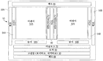
도 2는 도 1에 도시된 종래 기술의 비휘발성 메모리 셀을 사용하는 본 발명의 비휘발성 메모리 디바이스의 블록 다이어그램이다.
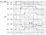
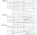
도 3a 및 도 3b는 각각 본 발명의 메모리 디바이스에서 사용하기 위한 프로그래밍/소거 및 판독 동작들의 파형도들이다.
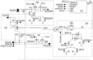
도 4a 및 도 4b는 각각 본 발명의 메모리 디바이스에서 사용하기 위한 네거티브/포지티브 워드 라인 디코더 회로(negative/positive word line decoder circuit) 및 네거티브 전하 펌프의 상세 회로 다이어그램들이다.
도 5는 본 발명의 메모리 디바이스에서 사용하기 위한 제1 네거티브/포지티브 고전압 디코더 회로의 상세 회로 다이어그램이다.
도 6은 본 발명의 메모리 디바이스에서 사용하기 위한 제2 네거티브/포지티브 고전압 디코더 회로의 상세 회로 다이어그램이다.
도 7은 본 발명의 메모리 디바이스에서 사용하기 위한 제3 네거티브/포지티브 고전압 디코더 회로의 상세 회로 다이어그램이다.
도 8은 본 발명의 메모리 디바이스와 함께 사용하기 위한 네거티브 전압 전하 펌프 발생기의 상세 회로 다이어그램이다.
도 9는 본 발명의 메모리 디바이스에서 사용하기 위한 네거티브 고전압 조정 회로(regulation circuit)의 상세 회로 다이어그램이다.
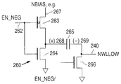
도 10은 본 발명의 메모리 디바이스에서 사용하기 위한 네거티브/포지티브 패드 회로(pad circuit)의 상세 회로 다이어그램이다.
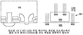
도 11a 및 도 11b는 종래 기술의 메모리 디바이스를 제조하는 데 사용하기 위한 종래 기술의 프로세스 흐름의 일부를 도시한 단면도들이다.
도 11c는 본 발명의 메모리 디바이스를 제조하기 위한 프로세스 흐름의 일부를 도시한 단면도이다.

Claims (40)
- 비휘발성 메모리 디바이스로서,
제1 도전성 타입의 반도체 기판; 및
복수의 행(row)들 및 열(column)들로 배열된 상기 반도체 기판 내의 비휘발성 메모리 셀들의 어레이를 포함하고, 각각의 메모리 셀은,
제2 도전성 타입의, 상기 반도체 기판의 표면 상의 제1 영역;
상기 제2 도전성 타입의, 상기 반도체 기판의 표면 상의 제2 영역;
상기 제1 영역과 상기 제2 영역 사이의 채널 영역;
상기 채널 영역의 제1 부분 위에 놓여 있고 그로부터 절연되며, 상기 제1 영역에 인접하고 상기 제1 영역과 거의 또는 전혀 중첩되지 않는 워드 라인;
상기 채널 영역의 제2 부분 위에 놓여 있고, 상기 제1 부분에 인접하고, 그로부터 절연되고 상기 제2 영역에 인접한 플로팅 게이트;
상기 플로팅 게이트 위에 놓인 커플링 게이트;
상기 제1 영역에 접속된 비트 라인;
제1 네거티브 전압을 생성하기 위한 네거티브 전하 펌프 회로; 및
커맨드 신호를 수신하고, 이에 응답하여, 복수의 제어 신호들을 생성하여 선택된 메모리 셀들의 커플링 게이트에 대한 상기 제1 네거티브 전압의 인가를 제어하기 위한 제어 회로를 포함하는, 비휘발성 메모리 디바이스. - 청구항 1에 있어서,
상기 복수의 제어 신호들은 소거 커맨드에 응답하여 생성되는, 비휘발성 메모리 디바이스. - 청구항 2에 있어서,
상기 네거티브 전하 펌프는 제2 네거티브 전압을 생성하고, 상기 제어 회로는 상기 제2 네거티브 전압을 비선택된 메모리 셀의 워드 라인에 인가하는, 비휘발성 메모리 디바이스. - 청구항 1에 있어서,
상기 복수의 제어 신호들은 판독 커맨드에 응답하여 셍성되는, 비휘발성 메모리 디바이스. - 청구항 1에 있어서,
상기 복수의 제어 신호들은 프로그래밍 커맨드에 응답하여 생성되는, 비휘발성 메모리 디바이스. - 청구항 1에 있어서,
상기 네거티브 전하 펌프는 상기 반도체 기판 내의 트리플 웰(triple well)에 있는, 비휘발성 메모리 디바이스. - 청구항 1에 있어서,
상기 메모리 셀들, 네거티브 전하 펌프, 및 제어 회로는 트윈 웰(twin well) P-sub CMOS 프로세스에서 제공되는 반도체 P 기판에 형성되는, 비휘발성 메모리 디바이스. - 청구항 1에 있어서,
상기 제어 회로는 네거티브 전압 다이오드-디코딩 회로를 포함하는, 비휘발성 메모리 디바이스. - 청구항 1에 있어서,
상기 제어 회로는 네거티브 레벨 시프터 회로(negative level shifter circuit) 및 클럭드 네거티브 부트스트래핑 회로(clocked negative bootstrapping circuit)를 포함하는, 비휘발성 메모리 디바이스. - 청구항 1에 있어서,
고전압 PMOS 트랜지스터와 고전압 NMOS 트랜지스터를 포함하는 네거티브 테스트 패드 회로(negative test pad circuit)를 추가로 포함하는, 비휘발성 메모리 디바이스. - 청구항 1에 있어서,
커패시터-디바이더(divider) 기반의 비교기를 갖는 네거티브 조정 회로(negative regulation circuit)를 추가로 포함하는, 비휘발성 메모리 디바이스. - 청구항 1에 있어서,
상기 제어 회로는 상기 메모리 셀들에 포지티브(positive) 또는 네거티브 고전압을 공급하기 위해 고전압 디코더에 전류 리미터(current limiter)를 포함하는, 비휘발성 메모리 디바이스. - 청구항 1에 있어서,
상기 제어 회로는 상기 메모리 셀들에 상기 워드 라인 상의 소거 전압을 공급하기 위해 고전압 디코더에 전류 리미터를 포함하는, 비휘발성 메모리 디바이스. - 청구항 1에 있어서,
상기 제어 회로는 상기 메모리 셀들의 커플링 게이트 상에 전압을 공급하기 위해 고전압 디코더에 전류 리미터를 포함하는, 비휘발성 메모리 디바이스. - 청구항 14에 있어서,
상기 제어 회로는 프로그래밍 또는 소거 동작 동안 상기 메모리 셀들의 커플링 게이트 상에 전압을 공급하기 위해 고전압 디코더에 전류 리미터를 포함하는, 비휘발성 메모리 디바이스. - 청구항 1에 있어서,
상기 제어 회로는 프로그래밍 또는 소거 또는 판독 동작에서 상기 메모리 셀들에 전압들을 공급하기 위해 고전압 디코더에 고전압 래치를 포함하는, 비휘발성 메모리 디바이스. - 청구항 1에 있어서,
상기 제어 회로는 프로그래밍 또는 소거 또는 판독 동작에서 상기 메모리 셀들에 전압들을 공급하기 위해 고전압 디코더에 고전압 레벨 시프터를 포함하는, 비휘발성 메모리 디바이스. - 청구항 1에 있어서,
상기 제어 회로는 프로그래밍 또는 소거 또는 판독 동작에서 상기 메모리 셀들에 전압들을 공급하기 위해 고전압 디코더에 저전압 래치를 포함하는, 비휘발성 메모리 디바이스. - 청구항 1에 있어서,
프로그래밍 또는 소거 또는 판독 동작에서 상기 메모리 셀들에 전압들을 공급하기 위한 저전압 디코더를 추가로 포함하는, 비휘발성 메모리 디바이스. - 청구항 19에 있어서,
상기 저전압 디코더는 프로그래밍, 소거, 또는 판독 동작에서 상기 메모리 셀들에 전압들을 공급하기 위한 워드 라인 드라이버에 절연 트랜지스터를 포함하는, 비휘발성 메모리 디바이스. - 청구항 1에 있어서,
각각의 메모리 셀은 분리형 게이트 플래시 메모리 셀인, 비휘발성 메모리 디바이스. - 청구항 20에 있어서,
각각의 메모리 셀은 팁 소거(tip erasing)를 갖는 분리형 게이트 플래시 메모리 셀인, 비휘발성 메모리 디바이스. - 청구항 20에 있어서,
각각의 메모리 셀은 상기 워드 라인으로부터 플로팅 게이트로의 팁 소거를 갖는 분리형 게이트 플래시 메모리 셀인, 비휘발성 메모리 디바이스. - 소정 타입의 비휘발성 메모리 디바이스를 동작시키는 방법으로서,
상기 비휘발성 메모리 디바이스는,
제1 도전성 타입의 반도체 기판; 및 복수의 행들 및 열들로 배열된 상기 반도체 기판 내의 비휘발성 메모리 셀들의 어레이를 갖고, 각각의 메모리 셀은, 제2 도전성 타입의, 상기 반도체 기판의 표면 상의 제1 영역; 상기 제2 도전성 타입의, 상기 반도체 기판의 표면 상의 제2 영역; 상기 제1 영역과 상기 제2 영역 사이의 채널 영역; 상기 채널 영역의 제1 부분 위에 놓여 있고 그로부터 절연되며, 상기 제1 영역에 인접하고 상기 제1 영역과 거의 또는 전혀 중첩되지 않는 워드 라인; 상기 채널 영역의 제2 부분 위에 놓여 있고, 상기 제1 부분에 인접하고, 그로부터 절연되고, 상기 제2 영역에 인접한 플로팅 게이트; 상기 플로팅 게이트 위에 놓인 커플링 게이트; 및 상기 제1 영역에 접속된 비트 라인을 갖고, 상기 방법은,
제1 네거티브 전압을 선택된 메모리 셀들의 상기 커플링 게이트에 인가하는 단계; 및
비네거티브 전압(non-negative voltage)을 상기 선택된 메모리 셀의 상기 워드 라인, 상기 비트 라인, 및 상기 제2 영역에 인가하는 단계를 포함하는, 방법. - 청구항 24에 있어서,
상기 방법은 상기 선택된 메모리 셀을 소거하기 위한 것인, 방법. - 청구항 25에 있어서,
0(zero) 전압이 상기 선택된 메모리 셀의 상기 비트 라인 및 제2 영역에 인가되고, 포지티브 전압이 상기 선택된 메모리 셀의 상기 워드 라인에 인가되는, 방법. - 청구항 26에 있어서,
다른 전압들이 상기 선택된 메모리 셀들의 상기 워드 라인 제2 영역에 인가되기 전에 상기 네거티브 전압이 상기 커플링 게이트에 인가되는, 방법. - 청구항 24에 있어서,
상기 선택된 메모리 셀들의 상기 커플링 게이트에 인가되는 상기 전압은 네거티브 전압인, 방법. - 청구항 24에 있어서,
상기 방법은 상기 선택된 메모리 셀을 판독하기 위한 것인, 방법. - 청구항 24에 있어서,
상기 방법은 상기 선택된 메모리 셀을 프로그래밍하기 위한 것인, 방법. - 청구항 30에 있어서,
상기 방법은 소스측 주입에 의해 상기 선택된 메모리 셀을 프로그래밍하기 위한 것인, 방법. - 청구항 24에 있어서,
비네거티브 전압을 상기 선택된 메모리 셀의 상기 워드 라인, 비트 라인, 커플링 게이트, 및 제2 영역에 인가하는 상기 방법은 오직 판독 및 프로그래밍의 동작만을 위한 것인, 방법. - 청구항 32에 있어서,
상기 방법은
소거 동작 동안 네거티브 전압을 비선택된 메모리 셀의 상기 커플링 게이트에 인가하는 단계를 추가로 포함하는, 방법. - 청구항 30에 있어서,
상기 방법은
프로그래밍 동작 동안 제2 네거티브 전압을 상기 선택된 메모리 셀의 상기 제2 영역에 인가하는 단계를 추가로 포함하는, 방법. - 청구항 33에 있어서,
상기 제2 네거티브 전압은 상기 제1 네거티브 전압과 상이한, 방법. - 청구항 32에 있어서,
상기 프로그래밍 동안, 상기 전압은 상기 전압이 상기 선택된 메모리 셀들의 상기 제2 영역에 인가된 후에 상기 커플링 게이트에 인가되는, 방법. - 청구항 25에 있어서,
상기 판독 동안, 상기 커플링 게이트에 인가되는 상기 전압은 상기 전압이 상기 선택된 메모리 셀들의 상기 워드 라인과 비트 라인에 인가되기 전에 인가되는, 방법. - 청구항 25에 있어서,
터널링(tunneling)은 상기 워드 라인으로부터 상기 플로팅 게이트까지인, 방법. - 청구항 38에 있어서,
상기 터널링은 워드라인 아크 영역으로부터 상기 플로팅 게이트까지인, 방법. - 청구항 38에 있어서,
상기 터널링은 상기 워드 라인으로부터 플로팅 게이트 팁 코너까지인, 방법.
Applications Claiming Priority (3)
| Application Number | Priority Date | Filing Date | Title |
|---|---|---|---|
| US14/506,433 | 2014-10-03 | ||
| US14/506,433 US9922715B2 (en) | 2014-10-03 | 2014-10-03 | Non-volatile split gate memory device and a method of operating same |
| PCT/US2015/050010 WO2016053607A1 (en) | 2014-10-03 | 2015-09-14 | A non-volatile split gate memory device and a method of operating same |
Publications (2)
| Publication Number | Publication Date |
|---|---|
| KR20170061160A true KR20170061160A (ko) | 2017-06-02 |
| KR101982948B1 KR101982948B1 (ko) | 2019-08-28 |
Family
ID=54200098
Family Applications (1)
| Application Number | Title | Priority Date | Filing Date |
|---|---|---|---|
| KR1020177011636A Active KR101982948B1 (ko) | 2014-10-03 | 2015-09-14 | 비휘발성 분리형 게이트 메모리 디바이스 및 그의 동작 방법 |
Country Status (7)
| Country | Link |
|---|---|
| US (2) | US9922715B2 (ko) |
| EP (1) | EP3201926A1 (ko) |
| JP (1) | JP6486462B2 (ko) |
| KR (1) | KR101982948B1 (ko) |
| CN (1) | CN107077891B (ko) |
| TW (1) | TWI641113B (ko) |
| WO (1) | WO2016053607A1 (ko) |
Cited By (2)
| Publication number | Priority date | Publication date | Assignee | Title |
|---|---|---|---|---|
| KR20200024310A (ko) * | 2017-08-25 | 2020-03-06 | 실리콘 스토리지 테크놀로지 인크 | 플래시 메모리 셀에서 데이터를 판독하기 위한 개선된 감지 증폭기 회로 |
| KR20210146995A (ko) * | 2019-04-29 | 2021-12-06 | 실리콘 스토리지 테크놀로지 인크 | 딥 러닝 인공 신경 네트워크 내의 아날로그 신경 메모리를 위한 디코딩 시스템 및 물리적 레이아웃 |
Families Citing this family (13)
| Publication number | Priority date | Publication date | Assignee | Title |
|---|---|---|---|---|
| US20160005749A1 (en) * | 2014-07-01 | 2016-01-07 | Qualcomm Incorporated | Series ferroelectric negative capacitor for multiple time programmable (mtp) devices |
| US9953719B2 (en) * | 2016-05-18 | 2018-04-24 | Silicon Storage Technology, Inc. | Flash memory cell and associated decoders |
| JP2019067474A (ja) * | 2017-10-05 | 2019-04-25 | 東芝メモリ株式会社 | 半導体記憶装置 |
| US11354562B2 (en) * | 2018-01-03 | 2022-06-07 | Silicon Storage Technology, Inc. | Programmable neuron for analog non-volatile memory in deep learning artificial neural network |
| US10847225B2 (en) * | 2018-06-20 | 2020-11-24 | Microchip Technology Incorporated | Split-gate flash memory cell with improved read performance |
| FR3095526B1 (fr) * | 2019-04-25 | 2022-04-22 | St Microelectronics Rousset | Procédé d’écriture dans une mémoire EEPROM et circuit intégré correspondant |
| US20210134369A1 (en) * | 2019-10-30 | 2021-05-06 | Sandisk Technologies Llc | Method for concurrent programming |
| US11081184B2 (en) | 2019-10-30 | 2021-08-03 | Sandisk Technologies Llc | Method of concurrent multi-state programming of non-volatile memory with bit line voltage step up |
| CN114335186B (zh) | 2020-09-30 | 2025-02-07 | 硅存储技术股份有限公司 | 具有设置在字线栅上方的擦除栅的分裂栅非易失性存储器单元及其制备方法 |
| US20220375952A1 (en) * | 2021-05-18 | 2022-11-24 | Silicon Storage Technology, Inc. | Non-volatile memory cell array formed in a p-well in a deep n-well in a p-substrate |
| KR102909427B1 (ko) * | 2021-05-18 | 2026-01-08 | 실리콘 스토리지 테크놀로지 인크 | P-기판의 깊은 n-웰 내 p-웰에 형성된 비휘발성 메모리 셀 어레이 |
| CN115775571A (zh) * | 2021-09-08 | 2023-03-10 | 合肥格易集成电路有限公司 | 存储器和存储器的操作方法 |
| CN120336256A (zh) * | 2025-04-17 | 2025-07-18 | 李修录 | 存算一体芯片及存储设备 |
Citations (4)
| Publication number | Priority date | Publication date | Assignee | Title |
|---|---|---|---|---|
| US20070070703A1 (en) * | 2005-09-26 | 2007-03-29 | Tran Hieu V | Flash memory array system including a top gate memory cell |
| US20100127308A1 (en) * | 2008-11-26 | 2010-05-27 | Nhan Do | Non-volatile memory cell with self aligned floating and erase gates, and method of making same |
| US20130242672A1 (en) * | 2012-03-13 | 2013-09-19 | Silicon Storage Technology, Inc. | Non-volatile Memory Device And A Method Of Operating Same |
| WO2014172433A1 (en) * | 2013-04-16 | 2014-10-23 | Silicon Storage Technology, Inc. | Non-volatile memory cell with self aligned floating and erase gates, and method of making same |
Family Cites Families (12)
| Publication number | Priority date | Publication date | Assignee | Title |
|---|---|---|---|---|
| KR19990088517A (ko) * | 1998-05-22 | 1999-12-27 | 마 유에 예일 | 비휘발성메모리셀구조및비휘발성메모리셀을작동시키는방법 |
| TW546840B (en) * | 2001-07-27 | 2003-08-11 | Hitachi Ltd | Non-volatile semiconductor memory device |
| DE10361718A1 (de) * | 2003-08-22 | 2005-03-17 | Hynix Semiconductor Inc., Ichon | Vorrichtung und Verfahren zum Steuern von nicht flüchtigem DRAM |
| US7145802B2 (en) | 2004-08-31 | 2006-12-05 | Skymedi Corporation | Programming and manufacturing method for split gate memory cell |
| JP2007207380A (ja) * | 2006-02-03 | 2007-08-16 | Renesas Technology Corp | 不揮発性半導体記憶装置 |
| US8138524B2 (en) * | 2006-11-01 | 2012-03-20 | Silicon Storage Technology, Inc. | Self-aligned method of forming a semiconductor memory array of floating memory cells with source side erase, and a memory array made thereby |
| JP2008287794A (ja) * | 2007-05-17 | 2008-11-27 | Renesas Technology Corp | 半導体集積回路およびその動作方法 |
| US8488388B2 (en) * | 2011-11-01 | 2013-07-16 | Silicon Storage Technology, Inc. | Method of programming a split gate non-volatile floating gate memory cell having a separate erase gate |
| US8804429B2 (en) * | 2011-12-08 | 2014-08-12 | Silicon Storage Technology, Inc. | Non-volatile memory device and a method of programming such device |
| US9472284B2 (en) * | 2012-11-19 | 2016-10-18 | Silicon Storage Technology, Inc. | Three-dimensional flash memory system |
| US9418744B2 (en) * | 2014-05-12 | 2016-08-16 | Silicon Storage Technology, Inc. | System and method to reduce disturbances during programming of flash memory cells |
| CN105609131A (zh) * | 2014-07-22 | 2016-05-25 | 硅存储技术公司 | 抑制擦除分裂栅闪存存储器单元扇区的部分的系统和方法 |
-
2014
- 2014-10-03 US US14/506,433 patent/US9922715B2/en active Active
-
2015
- 2015-09-14 WO PCT/US2015/050010 patent/WO2016053607A1/en not_active Ceased
- 2015-09-14 CN CN201580053591.1A patent/CN107077891B/zh active Active
- 2015-09-14 KR KR1020177011636A patent/KR101982948B1/ko active Active
- 2015-09-14 EP EP15771380.1A patent/EP3201926A1/en not_active Ceased
- 2015-09-14 JP JP2017518062A patent/JP6486462B2/ja active Active
- 2015-09-23 TW TW104131431A patent/TWI641113B/zh active
-
2016
- 2016-03-30 US US15/085,835 patent/US20160217864A1/en not_active Abandoned
Patent Citations (4)
| Publication number | Priority date | Publication date | Assignee | Title |
|---|---|---|---|---|
| US20070070703A1 (en) * | 2005-09-26 | 2007-03-29 | Tran Hieu V | Flash memory array system including a top gate memory cell |
| US20100127308A1 (en) * | 2008-11-26 | 2010-05-27 | Nhan Do | Non-volatile memory cell with self aligned floating and erase gates, and method of making same |
| US20130242672A1 (en) * | 2012-03-13 | 2013-09-19 | Silicon Storage Technology, Inc. | Non-volatile Memory Device And A Method Of Operating Same |
| WO2014172433A1 (en) * | 2013-04-16 | 2014-10-23 | Silicon Storage Technology, Inc. | Non-volatile memory cell with self aligned floating and erase gates, and method of making same |
Cited By (2)
| Publication number | Priority date | Publication date | Assignee | Title |
|---|---|---|---|---|
| KR20200024310A (ko) * | 2017-08-25 | 2020-03-06 | 실리콘 스토리지 테크놀로지 인크 | 플래시 메모리 셀에서 데이터를 판독하기 위한 개선된 감지 증폭기 회로 |
| KR20210146995A (ko) * | 2019-04-29 | 2021-12-06 | 실리콘 스토리지 테크놀로지 인크 | 딥 러닝 인공 신경 네트워크 내의 아날로그 신경 메모리를 위한 디코딩 시스템 및 물리적 레이아웃 |
Also Published As
| Publication number | Publication date |
|---|---|
| JP6486462B2 (ja) | 2019-03-20 |
| JP2017531896A (ja) | 2017-10-26 |
| US20160099067A1 (en) | 2016-04-07 |
| CN107077891B (zh) | 2021-03-30 |
| US9922715B2 (en) | 2018-03-20 |
| CN107077891A (zh) | 2017-08-18 |
| WO2016053607A1 (en) | 2016-04-07 |
| TW201618285A (zh) | 2016-05-16 |
| EP3201926A1 (en) | 2017-08-09 |
| TWI641113B (zh) | 2018-11-11 |
| US20160217864A1 (en) | 2016-07-28 |
| KR101982948B1 (ko) | 2019-08-28 |
Similar Documents
| Publication | Publication Date | Title |
|---|---|---|
| KR101982948B1 (ko) | 비휘발성 분리형 게이트 메모리 디바이스 및 그의 동작 방법 | |
| JP6911075B2 (ja) | 相補的電圧源を使用した分割ゲートフラッシュメモリシステム | |
| KR101538284B1 (ko) | 비휘발성 메모리 디바이스 및 그 동작 방법 | |
| KR20180042421A (ko) | 소스 라인 풀다운 회로로서 더미 메모리 셀을 사용하는 플래시 메모리 시스템 |
Legal Events
| Date | Code | Title | Description |
|---|---|---|---|
| A201 | Request for examination | ||
| PA0105 | International application |
Patent event date: 20170427 Patent event code: PA01051R01D Comment text: International Patent Application |
|
| PA0201 | Request for examination | ||
| PG1501 | Laying open of application | ||
| E902 | Notification of reason for refusal | ||
| PE0902 | Notice of grounds for rejection |
Comment text: Notification of reason for refusal Patent event date: 20180917 Patent event code: PE09021S01D |
|
| E701 | Decision to grant or registration of patent right | ||
| PE0701 | Decision of registration |
Patent event code: PE07011S01D Comment text: Decision to Grant Registration Patent event date: 20190328 |
|
| GRNT | Written decision to grant | ||
| PR0701 | Registration of establishment |
Comment text: Registration of Establishment Patent event date: 20190521 Patent event code: PR07011E01D |
|
| PR1002 | Payment of registration fee |
Payment date: 20190521 End annual number: 3 Start annual number: 1 |
|
| PG1601 | Publication of registration | ||
| FPAY | Annual fee payment |
Payment date: 20220422 Year of fee payment: 4 |
|
| PR1001 | Payment of annual fee |
Payment date: 20220422 Start annual number: 4 End annual number: 4 |
|
| PR1001 | Payment of annual fee |
Payment date: 20250507 Start annual number: 7 End annual number: 7 |