KR20170061868A - 미러 디스플레이 패널 - Google Patents
미러 디스플레이 패널 Download PDFInfo
- Publication number
- KR20170061868A KR20170061868A KR1020150166981A KR20150166981A KR20170061868A KR 20170061868 A KR20170061868 A KR 20170061868A KR 1020150166981 A KR1020150166981 A KR 1020150166981A KR 20150166981 A KR20150166981 A KR 20150166981A KR 20170061868 A KR20170061868 A KR 20170061868A
- Authority
- KR
- South Korea
- Prior art keywords
- disposed
- display panel
- gate
- pixel electrode
- front surface
- Prior art date
- Legal status (The legal status is an assumption and is not a legal conclusion. Google has not performed a legal analysis and makes no representation as to the accuracy of the status listed.)
- Granted
Links
Images




Classifications
-
- G—PHYSICS
- G02—OPTICS
- G02F—OPTICAL DEVICES OR ARRANGEMENTS FOR THE CONTROL OF LIGHT BY MODIFICATION OF THE OPTICAL PROPERTIES OF THE MEDIA OF THE ELEMENTS INVOLVED THEREIN; NON-LINEAR OPTICS; FREQUENCY-CHANGING OF LIGHT; OPTICAL LOGIC ELEMENTS; OPTICAL ANALOGUE/DIGITAL CONVERTERS
- G02F1/00—Devices or arrangements for the control of the intensity, colour, phase, polarisation or direction of light arriving from an independent light source, e.g. switching, gating or modulating; Non-linear optics
- G02F1/01—Devices or arrangements for the control of the intensity, colour, phase, polarisation or direction of light arriving from an independent light source, e.g. switching, gating or modulating; Non-linear optics for the control of the intensity, phase, polarisation or colour
- G02F1/13—Devices or arrangements for the control of the intensity, colour, phase, polarisation or direction of light arriving from an independent light source, e.g. switching, gating or modulating; Non-linear optics for the control of the intensity, phase, polarisation or colour based on liquid crystals, e.g. single liquid crystal display cells
- G02F1/133—Constructional arrangements; Operation of liquid crystal cells; Circuit arrangements
- G02F1/1333—Constructional arrangements; Manufacturing methods
- G02F1/1335—Structural association of cells with optical devices, e.g. polarisers or reflectors
- G02F1/133553—Reflecting elements
-
- G—PHYSICS
- G02—OPTICS
- G02F—OPTICAL DEVICES OR ARRANGEMENTS FOR THE CONTROL OF LIGHT BY MODIFICATION OF THE OPTICAL PROPERTIES OF THE MEDIA OF THE ELEMENTS INVOLVED THEREIN; NON-LINEAR OPTICS; FREQUENCY-CHANGING OF LIGHT; OPTICAL LOGIC ELEMENTS; OPTICAL ANALOGUE/DIGITAL CONVERTERS
- G02F1/00—Devices or arrangements for the control of the intensity, colour, phase, polarisation or direction of light arriving from an independent light source, e.g. switching, gating or modulating; Non-linear optics
- G02F1/01—Devices or arrangements for the control of the intensity, colour, phase, polarisation or direction of light arriving from an independent light source, e.g. switching, gating or modulating; Non-linear optics for the control of the intensity, phase, polarisation or colour
- G02F1/13—Devices or arrangements for the control of the intensity, colour, phase, polarisation or direction of light arriving from an independent light source, e.g. switching, gating or modulating; Non-linear optics for the control of the intensity, phase, polarisation or colour based on liquid crystals, e.g. single liquid crystal display cells
- G02F1/133—Constructional arrangements; Operation of liquid crystal cells; Circuit arrangements
- G02F1/1333—Constructional arrangements; Manufacturing methods
- G02F1/1335—Structural association of cells with optical devices, e.g. polarisers or reflectors
- G02F1/133509—Filters, e.g. light shielding masks
- G02F1/133514—Colour filters
-
- G—PHYSICS
- G02—OPTICS
- G02F—OPTICAL DEVICES OR ARRANGEMENTS FOR THE CONTROL OF LIGHT BY MODIFICATION OF THE OPTICAL PROPERTIES OF THE MEDIA OF THE ELEMENTS INVOLVED THEREIN; NON-LINEAR OPTICS; FREQUENCY-CHANGING OF LIGHT; OPTICAL LOGIC ELEMENTS; OPTICAL ANALOGUE/DIGITAL CONVERTERS
- G02F1/00—Devices or arrangements for the control of the intensity, colour, phase, polarisation or direction of light arriving from an independent light source, e.g. switching, gating or modulating; Non-linear optics
- G02F1/01—Devices or arrangements for the control of the intensity, colour, phase, polarisation or direction of light arriving from an independent light source, e.g. switching, gating or modulating; Non-linear optics for the control of the intensity, phase, polarisation or colour
- G02F1/13—Devices or arrangements for the control of the intensity, colour, phase, polarisation or direction of light arriving from an independent light source, e.g. switching, gating or modulating; Non-linear optics for the control of the intensity, phase, polarisation or colour based on liquid crystals, e.g. single liquid crystal display cells
- G02F1/133—Constructional arrangements; Operation of liquid crystal cells; Circuit arrangements
- G02F1/136—Liquid crystal cells structurally associated with a semi-conducting layer or substrate, e.g. cells forming part of an integrated circuit
- G02F1/1362—Active matrix addressed cells
- G02F1/136209—Light shielding layers, e.g. black matrix, incorporated in the active matrix substrate, e.g. structurally associated with the switching element
-
- G—PHYSICS
- G02—OPTICS
- G02F—OPTICAL DEVICES OR ARRANGEMENTS FOR THE CONTROL OF LIGHT BY MODIFICATION OF THE OPTICAL PROPERTIES OF THE MEDIA OF THE ELEMENTS INVOLVED THEREIN; NON-LINEAR OPTICS; FREQUENCY-CHANGING OF LIGHT; OPTICAL LOGIC ELEMENTS; OPTICAL ANALOGUE/DIGITAL CONVERTERS
- G02F1/00—Devices or arrangements for the control of the intensity, colour, phase, polarisation or direction of light arriving from an independent light source, e.g. switching, gating or modulating; Non-linear optics
- G02F1/01—Devices or arrangements for the control of the intensity, colour, phase, polarisation or direction of light arriving from an independent light source, e.g. switching, gating or modulating; Non-linear optics for the control of the intensity, phase, polarisation or colour
- G02F1/13—Devices or arrangements for the control of the intensity, colour, phase, polarisation or direction of light arriving from an independent light source, e.g. switching, gating or modulating; Non-linear optics for the control of the intensity, phase, polarisation or colour based on liquid crystals, e.g. single liquid crystal display cells
- G02F1/133—Constructional arrangements; Operation of liquid crystal cells; Circuit arrangements
- G02F1/136—Liquid crystal cells structurally associated with a semi-conducting layer or substrate, e.g. cells forming part of an integrated circuit
- G02F1/1362—Active matrix addressed cells
- G02F1/1368—Active matrix addressed cells in which the switching element is a three-electrode device
Landscapes
- Physics & Mathematics (AREA)
- Nonlinear Science (AREA)
- Mathematical Physics (AREA)
- Chemical & Material Sciences (AREA)
- Crystallography & Structural Chemistry (AREA)
- General Physics & Mathematics (AREA)
- Optics & Photonics (AREA)
- Engineering & Computer Science (AREA)
- Microelectronics & Electronic Packaging (AREA)
- Liquid Crystal (AREA)
Abstract
Description
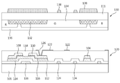
도 2는 도 1에 도시된 미러 디스플레이 패널을 나타내는 단면도이다.
도 3은 도 1에 도시된 미러 디스플레이 패널의 배면 반사층의 다른 형태를 나타내는 단면도이다.
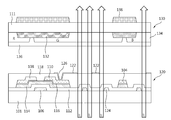
도 4a 및 도 4b는 도 2에 도시된 미러 디스플레이 패널의 투과 모드 및 미러 모드를 설명하기 위한 도면이다.
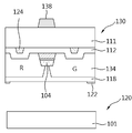
도 5는 본 발명의 제2 실시 예에 따른 미러 디스플레이 패널을 나타내는 단면도이다.
도 6은 도 5에 도시된 미러 디스플레이 패널의 다른 형태를 나타내는 단면도이다.
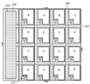
도 7은 게이트 구동 회로를 가지는 본 발명의 제1 및 제2 실시 예에 따른 미러 디스플레이 패널을 나타내는 평면도이다.
132 : 블랙매트릭스 134 : 컬러 필터
138 : 배면 반사층
Claims (8)
- 서로 대향하는 상부 및 하부 기판과;
상기 상부 및 하부 기판 중 어느 한 기판의 전면 상에 서로 교차하도록 배치된 게이트 라인 및 데이터 라인과;
상기 상부 기판의 배면인 사용자의 시청면 상에 상기 게이트 라인 및 데이터 라인과 중첩되도록 배치되는 배면 반사층을 구비하는 미러 디스플레이 패널. - 제 1 항에 있어서,
상기 하부 기판의 전면 상에 배치된 상기 게이트 라인 및 데이터 라인과 중첩되도록 상기 상부 기판의 전면 상에 배치되는 블랙매트릭스와;
상기 블랙매트릭스에 의해 마련된 화소 영역에 위치되도록 상기 상부 기판 상에 배치되는 컬러 필터를 더 구비하는 미러 디스플레이 패널. - 제 1 항에 있어서,
상기 게이트 라인 및 데이터 라인이 배치된 상기 상부 기판의 전면 상에 위치하는 컬러 필터를 더 구비하는 미러 디스플레이 패널. - 제 1 항에 있어서,
상기 게이트 라인 및 데이터 라인이 배치된 상기 하부 기판의 전면 상에 위치하는 컬러 필터를 더 구비하는 미러 디스플레이 패널. - 제 2 항 내지 제4 항 중 어느 한 항에 있어서,
상기 게이트 라인 및 데이터 라인과 접속된 박막트랜지스터와;
상기 박막트랜지스터와 접속된 화소 전극과;
상기 화소 전극과 전계를 이루는 공통 전극을 더 구비하며,
상기 배면 반사층은 상기 화소 전극 및 공통 전극 중 적어도 어느 하나와 중첩되는 미러 디스플레이 패널. - 제 5 항에 있어서,
상기 화소 전극 및 공통 전극 중 적어도 어느 하나는 불투명 금속으로 이루어지며,
상기 배면 반사층은 상기 불투명 금속으로 이루어진 전극과 중첩되는 미러 디스플레이 패널. - 제 1 항에 있어서,
상기 게이트 라인을 구동하도록 상기 게이트 라인과 동일한 기판 상에 배치되는 게이트 구동 회로를 더 구비하며,
상기 배면 반사층은 상기 게이트 구동 회로와 중첩되도록 배치되는 미러 디스플레이 패널. - 제 1 항에 있어서,
상기 배면 반사층은 MoTi, CuNx 및 Cr 중 적어도 어느 하나의 재질을 이용하여 단층 또는 복층 구조로 이루어지는 미러 디스플레이 패널.
Priority Applications (1)
| Application Number | Priority Date | Filing Date | Title |
|---|---|---|---|
| KR1020150166981A KR102522531B1 (ko) | 2015-11-27 | 2015-11-27 | 미러 디스플레이 패널 |
Applications Claiming Priority (1)
| Application Number | Priority Date | Filing Date | Title |
|---|---|---|---|
| KR1020150166981A KR102522531B1 (ko) | 2015-11-27 | 2015-11-27 | 미러 디스플레이 패널 |
Publications (2)
| Publication Number | Publication Date |
|---|---|
| KR20170061868A true KR20170061868A (ko) | 2017-06-07 |
| KR102522531B1 KR102522531B1 (ko) | 2023-04-17 |
Family
ID=59223545
Family Applications (1)
| Application Number | Title | Priority Date | Filing Date |
|---|---|---|---|
| KR1020150166981A Active KR102522531B1 (ko) | 2015-11-27 | 2015-11-27 | 미러 디스플레이 패널 |
Country Status (1)
| Country | Link |
|---|---|
| KR (1) | KR102522531B1 (ko) |
Cited By (2)
| Publication number | Priority date | Publication date | Assignee | Title |
|---|---|---|---|---|
| CN109659371A (zh) * | 2018-12-21 | 2019-04-19 | 武汉华星光电技术有限公司 | 薄膜晶体管、薄膜晶体管的制作方法和液晶显示屏 |
| US20220187662A1 (en) * | 2020-11-18 | 2022-06-16 | Innolux Corporation | Transparent display |
Citations (4)
| Publication number | Priority date | Publication date | Assignee | Title |
|---|---|---|---|---|
| JPH09329787A (ja) * | 1996-06-13 | 1997-12-22 | Seiko Instr Inc | 反射型液晶表示装置 |
| KR100207135B1 (ko) * | 1994-10-18 | 1999-07-15 | 니시무로 타이죠 | 반사형 액정표시소자 및 그 제조방법 |
| KR20080061107A (ko) * | 2006-12-28 | 2008-07-02 | 엘지디스플레이 주식회사 | 액정표시장치 및 그 제조방법 |
| KR20130015734A (ko) * | 2011-08-04 | 2013-02-14 | 엘지디스플레이 주식회사 | 액정표시장치 |
-
2015
- 2015-11-27 KR KR1020150166981A patent/KR102522531B1/ko active Active
Patent Citations (4)
| Publication number | Priority date | Publication date | Assignee | Title |
|---|---|---|---|---|
| KR100207135B1 (ko) * | 1994-10-18 | 1999-07-15 | 니시무로 타이죠 | 반사형 액정표시소자 및 그 제조방법 |
| JPH09329787A (ja) * | 1996-06-13 | 1997-12-22 | Seiko Instr Inc | 反射型液晶表示装置 |
| KR20080061107A (ko) * | 2006-12-28 | 2008-07-02 | 엘지디스플레이 주식회사 | 액정표시장치 및 그 제조방법 |
| KR20130015734A (ko) * | 2011-08-04 | 2013-02-14 | 엘지디스플레이 주식회사 | 액정표시장치 |
Cited By (3)
| Publication number | Priority date | Publication date | Assignee | Title |
|---|---|---|---|---|
| CN109659371A (zh) * | 2018-12-21 | 2019-04-19 | 武汉华星光电技术有限公司 | 薄膜晶体管、薄膜晶体管的制作方法和液晶显示屏 |
| US20220187662A1 (en) * | 2020-11-18 | 2022-06-16 | Innolux Corporation | Transparent display |
| US11733568B2 (en) * | 2020-11-18 | 2023-08-22 | Innolux Corporation | Transparent display |
Also Published As
| Publication number | Publication date |
|---|---|
| KR102522531B1 (ko) | 2023-04-17 |
Similar Documents
| Publication | Publication Date | Title |
|---|---|---|
| US10564479B2 (en) | Display device | |
| TWI463219B (zh) | 顯示裝置 | |
| US9429803B2 (en) | Logo patterning methods for liquid crystal displays | |
| US8049831B2 (en) | Liquid crystal display | |
| CN101276087B (zh) | 液晶显示装置 | |
| JP2008151817A (ja) | 半透過型液晶表示装置 | |
| KR100941866B1 (ko) | 듀얼 액정표시장치 | |
| CN105589246A (zh) | 弯曲显示装置 | |
| KR20090079779A (ko) | 듀얼 액정표시장치 | |
| KR20100000234A (ko) | 듀얼 액정표시장치 | |
| US10564495B2 (en) | Liquid crystal display device | |
| JP2007148347A (ja) | 液晶表示装置及びこれを利用した端末機 | |
| JP2005148740A (ja) | デュアルディスプレイの反射型液晶ディスプレイ | |
| JP2007148347A5 (ko) | ||
| CN110456580B (zh) | 一种显示基板及其控制方法、显示面板、显示装置 | |
| US20130278862A1 (en) | Liquid crystal display device | |
| US11018164B2 (en) | Thin-film transistor substrate, display panel, and display device | |
| KR102522531B1 (ko) | 미러 디스플레이 패널 | |
| WO2009113206A1 (ja) | 液晶表示装置 | |
| US8823900B2 (en) | Illumination device and electrooptic apparatus | |
| US11703729B2 (en) | Display device | |
| KR20180077940A (ko) | 보더리스타입 표시장치 | |
| JP2007133401A (ja) | 表示パネル及びこれを備えた表示装置 | |
| KR101679866B1 (ko) | 액정표시장치 | |
| KR101677995B1 (ko) | 반사투과형 액정표시장치 및 그 제조방법 |
Legal Events
| Date | Code | Title | Description |
|---|---|---|---|
| PA0109 | Patent application |
St.27 status event code: A-0-1-A10-A12-nap-PA0109 |
|
| PG1501 | Laying open of application |
St.27 status event code: A-1-1-Q10-Q12-nap-PG1501 |
|
| P22-X000 | Classification modified |
St.27 status event code: A-2-2-P10-P22-nap-X000 |
|
| R17-X000 | Change to representative recorded |
St.27 status event code: A-3-3-R10-R17-oth-X000 |
|
| A201 | Request for examination | ||
| PA0201 | Request for examination |
St.27 status event code: A-1-2-D10-D11-exm-PA0201 |
|
| R17-X000 | Change to representative recorded |
St.27 status event code: A-3-3-R10-R17-oth-X000 |
|
| D13-X000 | Search requested |
St.27 status event code: A-1-2-D10-D13-srh-X000 |
|
| D14-X000 | Search report completed |
St.27 status event code: A-1-2-D10-D14-srh-X000 |
|
| E902 | Notification of reason for refusal | ||
| PE0902 | Notice of grounds for rejection |
St.27 status event code: A-1-2-D10-D21-exm-PE0902 |
|
| AMND | Amendment | ||
| P11-X000 | Amendment of application requested |
St.27 status event code: A-2-2-P10-P11-nap-X000 |
|
| P13-X000 | Application amended |
St.27 status event code: A-2-2-P10-P13-nap-X000 |
|
| E601 | Decision to refuse application | ||
| PE0601 | Decision on rejection of patent |
St.27 status event code: N-2-6-B10-B15-exm-PE0601 |
|
| AMND | Amendment | ||
| P11-X000 | Amendment of application requested |
St.27 status event code: A-2-2-P10-P11-nap-X000 |
|
| P13-X000 | Application amended |
St.27 status event code: A-2-2-P10-P13-nap-X000 |
|
| PX0901 | Re-examination |
St.27 status event code: A-2-3-E10-E12-rex-PX0901 |
|
| PX0701 | Decision of registration after re-examination |
St.27 status event code: A-3-4-F10-F13-rex-PX0701 |
|
| X701 | Decision to grant (after re-examination) | ||
| GRNT | Written decision to grant | ||
| PR0701 | Registration of establishment |
St.27 status event code: A-2-4-F10-F11-exm-PR0701 |
|
| PR1002 | Payment of registration fee |
St.27 status event code: A-2-2-U10-U11-oth-PR1002 Fee payment year number: 1 |
|
| PG1601 | Publication of registration |
St.27 status event code: A-4-4-Q10-Q13-nap-PG1601 |
|
| PR1001 | Payment of annual fee |
St.27 status event code: A-4-4-U10-U11-oth-PR1001 Fee payment year number: 4 |
|
| U11 | Full renewal or maintenance fee paid |
Free format text: ST27 STATUS EVENT CODE: A-4-4-U10-U11-OTH-PR1001 (AS PROVIDED BY THE NATIONAL OFFICE) Year of fee payment: 4 |