KR20170062480A - 3차원 반도체 소자를 구비한 광전자 장치 - Google Patents
3차원 반도체 소자를 구비한 광전자 장치 Download PDFInfo
- Publication number
- KR20170062480A KR20170062480A KR1020177010463A KR20177010463A KR20170062480A KR 20170062480 A KR20170062480 A KR 20170062480A KR 1020177010463 A KR1020177010463 A KR 1020177010463A KR 20177010463 A KR20177010463 A KR 20177010463A KR 20170062480 A KR20170062480 A KR 20170062480A
- Authority
- KR
- South Korea
- Prior art keywords
- optoelectronic device
- group
- wire
- compounds
- semiconductor
- Prior art date
- Legal status (The legal status is an assumption and is not a legal conclusion. Google has not performed a legal analysis and makes no representation as to the accuracy of the status listed.)
- Granted
Links
Images


Classifications
-
- H—ELECTRICITY
- H10—SEMICONDUCTOR DEVICES; ELECTRIC SOLID-STATE DEVICES NOT OTHERWISE PROVIDED FOR
- H10F—INORGANIC SEMICONDUCTOR DEVICES SENSITIVE TO INFRARED RADIATION, LIGHT, ELECTROMAGNETIC RADIATION OF SHORTER WAVELENGTH OR CORPUSCULAR RADIATION
- H10F77/00—Constructional details of devices covered by this subclass
- H10F77/10—Semiconductor bodies
- H10F77/14—Shape of semiconductor bodies; Shapes, relative sizes or dispositions of semiconductor regions within semiconductor bodies
- H10F77/143—Shape of semiconductor bodies; Shapes, relative sizes or dispositions of semiconductor regions within semiconductor bodies comprising quantum structures
-
- H—ELECTRICITY
- H10—SEMICONDUCTOR DEVICES; ELECTRIC SOLID-STATE DEVICES NOT OTHERWISE PROVIDED FOR
- H10H—INORGANIC LIGHT-EMITTING SEMICONDUCTOR DEVICES HAVING POTENTIAL BARRIERS
- H10H20/00—Individual inorganic light-emitting semiconductor devices having potential barriers, e.g. light-emitting diodes [LED]
- H10H20/80—Constructional details
- H10H20/81—Bodies
- H10H20/811—Bodies having quantum effect structures or superlattices, e.g. tunnel junctions
-
- H01L33/04—
-
- H01L33/0054—
-
- H01L33/0062—
-
- H01L33/18—
-
- H—ELECTRICITY
- H10—SEMICONDUCTOR DEVICES; ELECTRIC SOLID-STATE DEVICES NOT OTHERWISE PROVIDED FOR
- H10H—INORGANIC LIGHT-EMITTING SEMICONDUCTOR DEVICES HAVING POTENTIAL BARRIERS
- H10H20/00—Individual inorganic light-emitting semiconductor devices having potential barriers, e.g. light-emitting diodes [LED]
- H10H20/01—Manufacture or treatment
- H10H20/011—Manufacture or treatment of bodies, e.g. forming semiconductor layers
- H10H20/013—Manufacture or treatment of bodies, e.g. forming semiconductor layers having light-emitting regions comprising only Group III-V materials
-
- H—ELECTRICITY
- H10—SEMICONDUCTOR DEVICES; ELECTRIC SOLID-STATE DEVICES NOT OTHERWISE PROVIDED FOR
- H10H—INORGANIC LIGHT-EMITTING SEMICONDUCTOR DEVICES HAVING POTENTIAL BARRIERS
- H10H20/00—Individual inorganic light-emitting semiconductor devices having potential barriers, e.g. light-emitting diodes [LED]
- H10H20/01—Manufacture or treatment
- H10H20/011—Manufacture or treatment of bodies, e.g. forming semiconductor layers
- H10H20/014—Manufacture or treatment of bodies, e.g. forming semiconductor layers having light-emitting regions comprising only Group IV materials
-
- H—ELECTRICITY
- H10—SEMICONDUCTOR DEVICES; ELECTRIC SOLID-STATE DEVICES NOT OTHERWISE PROVIDED FOR
- H10H—INORGANIC LIGHT-EMITTING SEMICONDUCTOR DEVICES HAVING POTENTIAL BARRIERS
- H10H20/00—Individual inorganic light-emitting semiconductor devices having potential barriers, e.g. light-emitting diodes [LED]
- H10H20/80—Constructional details
- H10H20/81—Bodies
- H10H20/811—Bodies having quantum effect structures or superlattices, e.g. tunnel junctions
- H10H20/812—Bodies having quantum effect structures or superlattices, e.g. tunnel junctions within the light-emitting regions, e.g. having quantum confinement structures
-
- H—ELECTRICITY
- H10—SEMICONDUCTOR DEVICES; ELECTRIC SOLID-STATE DEVICES NOT OTHERWISE PROVIDED FOR
- H10H—INORGANIC LIGHT-EMITTING SEMICONDUCTOR DEVICES HAVING POTENTIAL BARRIERS
- H10H20/00—Individual inorganic light-emitting semiconductor devices having potential barriers, e.g. light-emitting diodes [LED]
- H10H20/80—Constructional details
- H10H20/81—Bodies
- H10H20/817—Bodies characterised by the crystal structures or orientations, e.g. polycrystalline, amorphous or porous
- H10H20/818—Bodies characterised by the crystal structures or orientations, e.g. polycrystalline, amorphous or porous within the light-emitting regions
-
- H—ELECTRICITY
- H10—SEMICONDUCTOR DEVICES; ELECTRIC SOLID-STATE DEVICES NOT OTHERWISE PROVIDED FOR
- H10H—INORGANIC LIGHT-EMITTING SEMICONDUCTOR DEVICES HAVING POTENTIAL BARRIERS
- H10H20/00—Individual inorganic light-emitting semiconductor devices having potential barriers, e.g. light-emitting diodes [LED]
- H10H20/80—Constructional details
- H10H20/81—Bodies
- H10H20/819—Bodies characterised by their shape, e.g. curved or truncated substrates
- H10H20/82—Roughened surfaces, e.g. at the interface between epitaxial layers
-
- H—ELECTRICITY
- H10—SEMICONDUCTOR DEVICES; ELECTRIC SOLID-STATE DEVICES NOT OTHERWISE PROVIDED FOR
- H10H—INORGANIC LIGHT-EMITTING SEMICONDUCTOR DEVICES HAVING POTENTIAL BARRIERS
- H10H20/00—Individual inorganic light-emitting semiconductor devices having potential barriers, e.g. light-emitting diodes [LED]
- H10H20/80—Constructional details
- H10H20/81—Bodies
- H10H20/819—Bodies characterised by their shape, e.g. curved or truncated substrates
- H10H20/821—Bodies characterised by their shape, e.g. curved or truncated substrates of the light-emitting regions, e.g. non-planar junctions
Landscapes
- Led Devices (AREA)
Abstract
Description
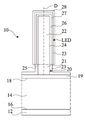
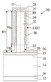
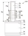
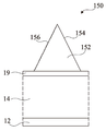
도 2는 마이크로와이어 또는 나노와이어를 포함하는 광전자 장치의 일 실시형태의 단순화된 부분 단면도이고;
도 3 및 도 4는 양자 도트를 포함하는 활성 영역의 일 나노와이어를 도시하는 단순화된 부분확대도이고;
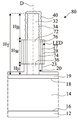
도 5 내지 도 9는 마이크로와이어 또는 나노와이어를 포함하는 광전자 장치의 실시형태의 단순화된 부분 단면도이고;
도 10 내지 도 13은 마이크로와이어 또는 나노와이어를 포함하는 광전자 장치의 실시형태의 중간 제조 단계에서 얻어지는 구조의 단순화된 부분 단면도이다.
Claims (13)
- III-V족 화합물, II-VI족 화합물, 및 IV족 화합물을 포함하는 그룹으로부터 선택된 제 1 화합물로 주로 제조된 3차원 반도체 소자(20; 152)를 포함하고, 각각의 상기 반도체 소자는, 선택적으로 상기 반도체 소자를 부분적으로 피복하는 절연 부분으로, 서로에 대해 경사진 연속 패싯(facet)들을 포함하는 적어도 제 1 표면(34)을 형성하는 광전자 장치(30)로서,
상기 광전자 장치는 상기 패싯들 사이의 적어도 일부의 이음부(seam; 42)에 양자 도트(quantum dot; 60)를 포함하고, 상기 양자 도트는 상기 제 1 화합물과 추가 원소의 혼합물로 주로 제조되며, 제 1 파장의 제 1 전자기 복사를 방출 또는 수신할 수 있는,
광전자 장치. - 제 1 항에 있어서,
하나 이상의 단일 양자 우물 또는 다중 양자 우물을 포함하는, 그리고 상기 제 1 파장과 상이한 제 2 파장의 제 2 전자기 복사를 방출 또는 수신할 수 있는 활성층(62; 76)을 더 포함하는,
광전자 장치. - 제 1 항 또는 제 2 항에 있어서,
상기 제 1 표면(34)과 구별되는 제 2 표면(74)을 포함하고, 상기 활성층(76)은 상기 제 2 표면을 피복하는,
광전자 장치. - 제 1 항 또는 제 2 항에 있어서,
상기 활성층(62)은 상기 양자 도트(60)를 피복하는,
광전자 장치. - 제 1 항 내지 제 4 항 중 어느 한 항에 있어서,
각각의 양자 도트(60)는 InxAlyGa1 -x- yN 화합물로 주로 제조되고, 여기서, 0 ≤ x ≤ 1, 0 ≤ y ≤ 1 및 1-x-y > 0인,
광전자 장치. - 제 1 항 내지 제 5 항 중 어느 한 항에 있어서,
상기 반도체 소자(20)는 나노와이어, 마이크로와이어, 및/또는 나노미터 범위 또는 마이크로미터 범위의 피라미드 구조인,
광전자 장치. - 제 1 항 내지 제 6 항 중 어느 한 항에 있어서,
상기 반도체 소자는 우선 방향을 따라 연장된 형상을 갖고, 인접한 이음부 쌍들 중 2 개의 이음부(42)들 사이에서 상기 우선 방향에 수직으로 측정된 거리는 5 nm를 초과하는,
광전자 장치. - 제 7 항에 있어서,
상기 우선 방향에 평행으로 측정된 2 개의 인접한 이음부(42)들 사이의 거리는 1 μm 미만인,
광전자 장치. - 제 7 항에 있어서,
상기 이음부(42)들의 밀도는 108 이음부/cm2을 초과하는,
광전자 장치. - 광전자 장치(30)를 제조하는 방법으로서,
III-V족 화합물, II-VI족 화합물, 및 IV족 화합물을 포함하는 그룹으로부터 선택되는 제 1 화합물로 주로 제조된 3차원 반도체 소자(20; 152)를 형성하는 단계 - 각각의 반도체 소자는, 선택적으로 상기 반도체 소자를 부분적으로 피복하는 절연 부분으로, 서로에 대해 경사진 연속 패싯(facet)들을 포함하는 하나 이상의 제 1 표면(34)을 형성함 -; 및
패싯들 사이의 적어도 일부의 이음부(42)에 양자 도트(60)를 형성하는 단계를 포함하고, 상기 양자 도트는 상기 제 1 화합물과 추가 원소의 혼합물로 주로 제조되며, 제 1 파장의 제 1 전자기 복사를 방출 또는 수신할 수 있는,
광전자 장치를 제조하는 방법. - 제 10 항에 있어서,
하나 이상의 단일 양자 우물 또는 다중 양자 우물을 포함하는, 그리고 상기 제 1 파장과 상이한 제 2 파장의 제 2 전자기 복사를 방출 또는 수신할 수 있는 활성층(62; 76)을 형성하는 단계를 더 포함하는,
광전자 장치를 제조하는 방법. - 제 10 항 또는 제 11 항에 있어서,
반도체 소자(20)를 형성하는 단계 및 상기 제 1 표면(34)을 형성하기 위해 상기 반도체 소자를 부분적으로 에칭하는 단계를 포함하는,
광전자 장치를 제조하는 방법. - 제 10 항 또는 제 11 항에 있어서,
상기 제 1 표면은 상기 반도체 소자(20)의 성장과 동시에 형성되는,
광전자 장치를 제조하는 방법.
Applications Claiming Priority (3)
| Application Number | Priority Date | Filing Date | Title |
|---|---|---|---|
| FR1459275 | 2014-09-30 | ||
| FR1459275A FR3026564B1 (fr) | 2014-09-30 | 2014-09-30 | Dispositif optoelectronique a elements semiconducteurs tridimensionnels |
| PCT/FR2015/052602 WO2016051078A1 (fr) | 2014-09-30 | 2015-09-29 | Dispositif optoelectronique a elements semiconducteurs tridimensionnels |
Publications (2)
| Publication Number | Publication Date |
|---|---|
| KR20170062480A true KR20170062480A (ko) | 2017-06-07 |
| KR102389679B1 KR102389679B1 (ko) | 2022-04-21 |
Family
ID=52684308
Family Applications (1)
| Application Number | Title | Priority Date | Filing Date |
|---|---|---|---|
| KR1020177010463A Active KR102389679B1 (ko) | 2014-09-30 | 2015-09-29 | 3차원 반도체 소자를 구비한 광전자 장치 |
Country Status (6)
| Country | Link |
|---|---|
| US (1) | US10615299B2 (ko) |
| EP (1) | EP3201951B1 (ko) |
| KR (1) | KR102389679B1 (ko) |
| CN (1) | CN107078186B (ko) |
| FR (1) | FR3026564B1 (ko) |
| WO (1) | WO2016051078A1 (ko) |
Cited By (1)
| Publication number | Priority date | Publication date | Assignee | Title |
|---|---|---|---|---|
| KR20180112764A (ko) * | 2015-11-30 | 2018-10-12 | 꼼미사리아 아 레네르지 아토미끄 에뜨 옥스 에너지스 앨터네이티브즈 | 축방향 구성의 3차원 반도체 구조를 포함하는 광전자 소자 |
Families Citing this family (6)
| Publication number | Priority date | Publication date | Assignee | Title |
|---|---|---|---|---|
| FR3076399B1 (fr) * | 2017-12-28 | 2020-01-24 | Aledia | Dispositif optoelectronique comprenant des diodes electroluminescentes tridimensionnelles |
| FR3096509B1 (fr) * | 2019-05-20 | 2021-05-28 | Aledia | Dispositif optoelectronique avec diodes electroluminescentes dont une zone dopee integre une portion externe a base d’aluminium et de nitrure de galium |
| FR3098013B1 (fr) * | 2019-06-25 | 2021-07-02 | Commissariat Energie Atomique | Procédé de fabrication d'un dispositif optoélectronique à diodes électroluminescentes de type axial |
| DE102021109960A1 (de) * | 2021-04-20 | 2022-10-20 | OSRAM Opto Semiconductors Gesellschaft mit beschränkter Haftung | Strahlungsemittierender halbleiterchip und verfahren zur herstellung eines strahlungsemittierenden halbleiterchips |
| CN114843383B (zh) * | 2022-07-01 | 2022-10-25 | 季华实验室 | Led结构及其制造方法、led显示屏 |
| CN118712294B (zh) * | 2024-08-29 | 2024-11-15 | 山东省科学院激光研究所 | 一种纳米发光二极管及其制备方法 |
Citations (2)
| Publication number | Priority date | Publication date | Assignee | Title |
|---|---|---|---|---|
| US20050269286A1 (en) * | 2004-06-08 | 2005-12-08 | Manish Sharma | Method of fabricating a nano-wire |
| KR20110063799A (ko) * | 2008-09-01 | 2011-06-14 | 가꼬호징 조찌가꾸잉 | 반도체 광소자 어레이 및 그의 제조방법 |
Family Cites Families (10)
| Publication number | Priority date | Publication date | Assignee | Title |
|---|---|---|---|---|
| FR1459275A (fr) | 1965-10-07 | 1966-04-29 | Lambert & Cie Soc | Perfectionnement aux installations pour le dosage des agrégats |
| KR100736515B1 (ko) * | 2005-12-01 | 2007-07-06 | 삼성전자주식회사 | 다공성 템플릿을 이용한 나노 와이어의 제조방법 및나노와이어 구조체 |
| US20100259184A1 (en) * | 2006-02-24 | 2010-10-14 | Ryou Kato | Light-emitting device |
| US8138493B2 (en) * | 2008-07-09 | 2012-03-20 | Qunano Ab | Optoelectronic semiconductor device |
| US8669544B2 (en) * | 2011-02-10 | 2014-03-11 | The Royal Institution For The Advancement Of Learning/Mcgill University | High efficiency broadband semiconductor nanowire devices and methods of fabricating without foreign catalysis |
| CN102280545A (zh) * | 2011-08-17 | 2011-12-14 | 中国科学院苏州纳米技术与纳米仿生研究所 | 硅基光发射器件及其制备方法 |
| US8835965B2 (en) * | 2012-01-18 | 2014-09-16 | The Penn State Research Foundation | Application of semiconductor quantum dot phosphors in nanopillar light emitting diodes |
| FR2995729B1 (fr) | 2012-09-18 | 2016-01-01 | Aledia | Dispositif opto-electrique a microfils ou nanofils semiconducteurs et son procede de fabrication |
| FR2997558B1 (fr) | 2012-10-26 | 2015-12-18 | Aledia | Dispositif opto-electrique et son procede de fabrication |
| EP2912699B1 (en) * | 2012-10-26 | 2019-12-18 | Glo Ab | Method for modifying selected portions of nanowire sized opto-electronic structure |
-
2014
- 2014-09-30 FR FR1459275A patent/FR3026564B1/fr not_active Expired - Fee Related
-
2015
- 2015-09-29 KR KR1020177010463A patent/KR102389679B1/ko active Active
- 2015-09-29 CN CN201580053007.2A patent/CN107078186B/zh active Active
- 2015-09-29 EP EP15788111.1A patent/EP3201951B1/fr active Active
- 2015-09-29 US US15/513,797 patent/US10615299B2/en active Active
- 2015-09-29 WO PCT/FR2015/052602 patent/WO2016051078A1/fr not_active Ceased
Patent Citations (2)
| Publication number | Priority date | Publication date | Assignee | Title |
|---|---|---|---|---|
| US20050269286A1 (en) * | 2004-06-08 | 2005-12-08 | Manish Sharma | Method of fabricating a nano-wire |
| KR20110063799A (ko) * | 2008-09-01 | 2011-06-14 | 가꼬호징 조찌가꾸잉 | 반도체 광소자 어레이 및 그의 제조방법 |
Cited By (1)
| Publication number | Priority date | Publication date | Assignee | Title |
|---|---|---|---|---|
| KR20180112764A (ko) * | 2015-11-30 | 2018-10-12 | 꼼미사리아 아 레네르지 아토미끄 에뜨 옥스 에너지스 앨터네이티브즈 | 축방향 구성의 3차원 반도체 구조를 포함하는 광전자 소자 |
Also Published As
| Publication number | Publication date |
|---|---|
| WO2016051078A1 (fr) | 2016-04-07 |
| EP3201951B1 (fr) | 2019-11-27 |
| FR3026564B1 (fr) | 2018-02-16 |
| US10615299B2 (en) | 2020-04-07 |
| EP3201951A1 (fr) | 2017-08-09 |
| FR3026564A1 (fr) | 2016-04-01 |
| CN107078186A (zh) | 2017-08-18 |
| US20180233610A1 (en) | 2018-08-16 |
| CN107078186B (zh) | 2019-10-11 |
| KR102389679B1 (ko) | 2022-04-21 |
Similar Documents
| Publication | Publication Date | Title |
|---|---|---|
| US9728679B2 (en) | Optoelectronic device and method for manufacturing same | |
| US10651341B2 (en) | Optoelectronic device and method for manufacturing same | |
| US10050080B2 (en) | Optoelectronic device and method for manufacturing same | |
| KR102389679B1 (ko) | 3차원 반도체 소자를 구비한 광전자 장치 | |
| US8134170B2 (en) | Nitride semiconductor light emitting device and method of manufacturing the same | |
| US9537050B2 (en) | Optoelectronic device and method for manufacturing same | |
| KR102279462B1 (ko) | 광 추출효율이 향상된 발광 다이오드를 구비하는 광전자 디바이스 | |
| US10510535B2 (en) | Optoelectronic device comprising three-dimensional semiconductor elements, and method for manufacturing said device | |
| WO2024042221A1 (en) | Nanostructure/microstructure device | |
| US11049997B2 (en) | Optoelectronic device comprising three-dimensional semiconductor structures with a wider single-crystal portion | |
| US20170365737A1 (en) | Optoelectronic device comprising three-dimensional semiconductor elements and method for the production thereof | |
| JP7621635B2 (ja) | 三次元発光ダイオードを備えた光電子デバイス | |
| US10026870B2 (en) | Optoelectronic device having semiconductor elements | |
| KR102865808B1 (ko) | 발광 다이오드 및 제조 방법 | |
| US12206040B2 (en) | Method for homogenising the cross-section of nanowires for light-emitting diodes |
Legal Events
| Date | Code | Title | Description |
|---|---|---|---|
| PA0105 | International application |
St.27 status event code: A-0-1-A10-A15-nap-PA0105 |
|
| PG1501 | Laying open of application |
St.27 status event code: A-1-1-Q10-Q12-nap-PG1501 |
|
| R18-X000 | Changes to party contact information recorded |
St.27 status event code: A-3-3-R10-R18-oth-X000 |
|
| A201 | Request for examination | ||
| PA0201 | Request for examination |
St.27 status event code: A-1-2-D10-D11-exm-PA0201 |
|
| R18-X000 | Changes to party contact information recorded |
St.27 status event code: A-3-3-R10-R18-oth-X000 |
|
| D13-X000 | Search requested |
St.27 status event code: A-1-2-D10-D13-srh-X000 |
|
| D14-X000 | Search report completed |
St.27 status event code: A-1-2-D10-D14-srh-X000 |
|
| E902 | Notification of reason for refusal | ||
| PE0902 | Notice of grounds for rejection |
St.27 status event code: A-1-2-D10-D21-exm-PE0902 |
|
| E13-X000 | Pre-grant limitation requested |
St.27 status event code: A-2-3-E10-E13-lim-X000 |
|
| P11-X000 | Amendment of application requested |
St.27 status event code: A-2-2-P10-P11-nap-X000 |
|
| P13-X000 | Application amended |
St.27 status event code: A-2-2-P10-P13-nap-X000 |
|
| E701 | Decision to grant or registration of patent right | ||
| PE0701 | Decision of registration |
St.27 status event code: A-1-2-D10-D22-exm-PE0701 |
|
| GRNT | Written decision to grant | ||
| PR0701 | Registration of establishment |
St.27 status event code: A-2-4-F10-F11-exm-PR0701 |
|
| PR1002 | Payment of registration fee |
St.27 status event code: A-2-2-U10-U12-oth-PR1002 Fee payment year number: 1 |
|
| PG1601 | Publication of registration |
St.27 status event code: A-4-4-Q10-Q13-nap-PG1601 |
|
| P22-X000 | Classification modified |
St.27 status event code: A-4-4-P10-P22-nap-X000 |
|
| PR1001 | Payment of annual fee |
St.27 status event code: A-4-4-U10-U11-oth-PR1001 Fee payment year number: 4 |
|
| R18 | Changes to party contact information recorded |
Free format text: ST27 STATUS EVENT CODE: A-5-5-R10-R18-OTH-X000 (AS PROVIDED BY THE NATIONAL OFFICE) |
|
| R18-X000 | Changes to party contact information recorded |
St.27 status event code: A-5-5-R10-R18-oth-X000 |
|
| R18 | Changes to party contact information recorded |
Free format text: ST27 STATUS EVENT CODE: A-5-5-R10-R18-OTH-X000 (AS PROVIDED BY THE NATIONAL OFFICE) |
|
| R18-X000 | Changes to party contact information recorded |
St.27 status event code: A-5-5-R10-R18-oth-X000 |
|
| PR1001 | Payment of annual fee |
St.27 status event code: A-4-4-U10-U11-oth-PR1001 Fee payment year number: 5 |
|
| U11 | Full renewal or maintenance fee paid |
Free format text: ST27 STATUS EVENT CODE: A-4-4-U10-U11-OTH-PR1001 (AS PROVIDED BY THE NATIONAL OFFICE) Year of fee payment: 5 |