KR20170063009A - 액정 표시 장치 - Google Patents
액정 표시 장치 Download PDFInfo
- Publication number
- KR20170063009A KR20170063009A KR1020150168907A KR20150168907A KR20170063009A KR 20170063009 A KR20170063009 A KR 20170063009A KR 1020150168907 A KR1020150168907 A KR 1020150168907A KR 20150168907 A KR20150168907 A KR 20150168907A KR 20170063009 A KR20170063009 A KR 20170063009A
- Authority
- KR
- South Korea
- Prior art keywords
- dummy
- common
- electrode
- pixel
- line
- Prior art date
- Legal status (The legal status is an assumption and is not a legal conclusion. Google has not performed a legal analysis and makes no representation as to the accuracy of the status listed.)
- Granted
Links
Images


Classifications
-
- G—PHYSICS
- G02—OPTICS
- G02F—OPTICAL DEVICES OR ARRANGEMENTS FOR THE CONTROL OF LIGHT BY MODIFICATION OF THE OPTICAL PROPERTIES OF THE MEDIA OF THE ELEMENTS INVOLVED THEREIN; NON-LINEAR OPTICS; FREQUENCY-CHANGING OF LIGHT; OPTICAL LOGIC ELEMENTS; OPTICAL ANALOGUE/DIGITAL CONVERTERS
- G02F1/00—Devices or arrangements for the control of the intensity, colour, phase, polarisation or direction of light arriving from an independent light source, e.g. switching, gating or modulating; Non-linear optics
- G02F1/01—Devices or arrangements for the control of the intensity, colour, phase, polarisation or direction of light arriving from an independent light source, e.g. switching, gating or modulating; Non-linear optics for the control of the intensity, phase, polarisation or colour
- G02F1/13—Devices or arrangements for the control of the intensity, colour, phase, polarisation or direction of light arriving from an independent light source, e.g. switching, gating or modulating; Non-linear optics for the control of the intensity, phase, polarisation or colour based on liquid crystals, e.g. single liquid crystal display cells
- G02F1/133—Constructional arrangements; Operation of liquid crystal cells; Circuit arrangements
- G02F1/1333—Constructional arrangements; Manufacturing methods
- G02F1/1343—Electrodes
- G02F1/134309—Electrodes characterised by their geometrical arrangement
- G02F1/134363—Electrodes characterised by their geometrical arrangement for applying an electric field parallel to the substrate, i.e. in-plane switching [IPS]
-
- G—PHYSICS
- G02—OPTICS
- G02F—OPTICAL DEVICES OR ARRANGEMENTS FOR THE CONTROL OF LIGHT BY MODIFICATION OF THE OPTICAL PROPERTIES OF THE MEDIA OF THE ELEMENTS INVOLVED THEREIN; NON-LINEAR OPTICS; FREQUENCY-CHANGING OF LIGHT; OPTICAL LOGIC ELEMENTS; OPTICAL ANALOGUE/DIGITAL CONVERTERS
- G02F1/00—Devices or arrangements for the control of the intensity, colour, phase, polarisation or direction of light arriving from an independent light source, e.g. switching, gating or modulating; Non-linear optics
- G02F1/01—Devices or arrangements for the control of the intensity, colour, phase, polarisation or direction of light arriving from an independent light source, e.g. switching, gating or modulating; Non-linear optics for the control of the intensity, phase, polarisation or colour
- G02F1/13—Devices or arrangements for the control of the intensity, colour, phase, polarisation or direction of light arriving from an independent light source, e.g. switching, gating or modulating; Non-linear optics for the control of the intensity, phase, polarisation or colour based on liquid crystals, e.g. single liquid crystal display cells
- G02F1/133—Constructional arrangements; Operation of liquid crystal cells; Circuit arrangements
- G02F1/136—Liquid crystal cells structurally associated with a semi-conducting layer or substrate, e.g. cells forming part of an integrated circuit
- G02F1/1362—Active matrix addressed cells
- G02F1/136286—Wiring, e.g. gate line, drain line
Landscapes
- Physics & Mathematics (AREA)
- Nonlinear Science (AREA)
- Mathematical Physics (AREA)
- Chemical & Material Sciences (AREA)
- Crystallography & Structural Chemistry (AREA)
- General Physics & Mathematics (AREA)
- Optics & Photonics (AREA)
- Engineering & Computer Science (AREA)
- Microelectronics & Electronic Packaging (AREA)
- Geometry (AREA)
- Liquid Crystal (AREA)
- Devices For Indicating Variable Information By Combining Individual Elements (AREA)
Abstract
Description
도 2는 종래의 액정 표시 장치의 액티브 영역과 더미 영역 경계를 확대하여 나타낸 도면이다.
도 3은 본 발명에 따른 액정 표시 장치의 액티브 영역에 구비된 화소 및 더미 영역에 구비된 더미 화소를 하나씩 확대하여 나타낸 도면이다.
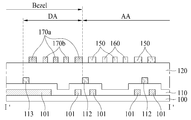
도 4는 도 3에 도시된 "I'-I'"라인을 따라 절취한 본 발명에 따른 액정 표시 장치의 단면도이다.
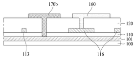
도 5는 도 3에 도시된 "I″-I″"라인을 따라 절취한 본 발명에 따른 액정 표시 장치의 단면도이다.
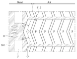
도 6은 본 발명에 따른 액정 표시 장치의 액티브 영역과 더미 영역 경계를 확대하여 나타낸 도면이다.
102: 게이트 전극 103: 게이트 라인
110: 절연막 112: 데이터 라인
113: 더미 데이터 라인 120: 평탄화층
150: 공통 전극 160: 화소 전극
170a: 더미 공통 전극 170b: 더미 화소 전극
Claims (8)
- 영상이 표시되는 액티브 영역에서 서로 교차하는 복수의 게이트 라인과 복수의 데이터 라인에 의해 정의되는 복수의 화소;
상기 액티브 영역 외곽의 베젤 영역에 구비되는 더미 화소; 및
상기 복수의 화소 및 상기 더미 화소와 전기적으로 연결되어 상기 복수의 화소 및 상기 더미 화소로 공통 전압을 인가하는 공통 라인이 구비되고,
상기 공통 라인은, 소정의 영역에서 상기 더미 화소와 오버랩되도록 구비된, 액정 표시 장치. - 제1항에 있어서,
상기 복수의 화소에는, 동일한 층에 구비되어 전계를 발생시키는 화소 전극 및 공통 전극이 구비되고,
상기 더미 화소에는, 상기 화소 전극과 동일한 구조로 동일한 층에 구비된 더미 화소 전극 및 상기 공통 전극과 동일한 구조로 동일한 층에 구비된 더미 공통 전극이 구비된, 액정 표시 장치. - 제2항에 있어서,
상기 공통 라인은, 상기 더미 화소 내부에서 상기 더미 화소 전극과 오버랩되도록 구비된, 액정 표시 장치. - 제2항에 있어서,
상기 더미 화소 전극 및 상기 더미 공통 전극은 콘택홀을 통해 상기 공통 라인에 연결된, 액정 표시 장치. - 제1항에 있어서,
상기 공통 라인은 온도 변화시 팽창에 의한 손상을 방지할 수 있도록 내부에 개구부가 구비된, 액정 표시 장치. - 제1항에 있어서,
상기 공통 라인은,
상기 게이트 라인과 평행하게 구비되어 상기 복수의 화소 및 상기 더미 화소로 상기 공통 전압을 각각 인가하는 복수의 제1공통 라인; 및
상기 복수의 제1공통 라인과 연결되어 상기 복수의 제1공통 라인으로 상기 공통 전압을 인가하는 제2공통 라인을 포함하여 구비되고,
상기 제2공통 라인은, 상기 소정의 영역에서 상기 더미 화소와 오버랩되도록 구비된, 액정 표시 장치. - 제6항에 있어서,
상기 복수의 화소에는, 동일한 층에 구비되어 전계를 발생시키는 화소 전극 및 공통 전극이 구비되고,
상기 더미 화소에는, 상기 화소 전극과 동일한 구조로 동일한 층에 구비된 더미 화소 전극 및 상기 공통 전극과 동일한 구조로 동일한 층에 구비된 더미 공통 전극이 구비되고,
상기 화소 전극, 상기 더미 화소 전극, 상기 공통 전극, 상기 더미 공통 전극 및 상기 데이터 라인은 각 화소 또는 각 더미 화소의 중앙부를 기준으로 대칭적으로 꺾인 구조를 갖고,
상기 제2공통 라인은 상기 액티브 영역의 최외곽에 구비된 화소를 정의하는 데이터 라인 보다 외곽에 구비된, 액정 표시 장치. - 제1항에 있어서,
상기 더미 화소는 상기 데이터 라인과 동일한 구조로 동일한 층에 구비된 더미 데이터 라인, 및 상기 복수의 게이트 라인에 의해 정의된, 액정 표시 장치.
Priority Applications (1)
| Application Number | Priority Date | Filing Date | Title |
|---|---|---|---|
| KR1020150168907A KR102387860B1 (ko) | 2015-11-30 | 2015-11-30 | 액정 표시 장치 |
Applications Claiming Priority (1)
| Application Number | Priority Date | Filing Date | Title |
|---|---|---|---|
| KR1020150168907A KR102387860B1 (ko) | 2015-11-30 | 2015-11-30 | 액정 표시 장치 |
Publications (2)
| Publication Number | Publication Date |
|---|---|
| KR20170063009A true KR20170063009A (ko) | 2017-06-08 |
| KR102387860B1 KR102387860B1 (ko) | 2022-04-15 |
Family
ID=59221494
Family Applications (1)
| Application Number | Title | Priority Date | Filing Date |
|---|---|---|---|
| KR1020150168907A Active KR102387860B1 (ko) | 2015-11-30 | 2015-11-30 | 액정 표시 장치 |
Country Status (1)
| Country | Link |
|---|---|
| KR (1) | KR102387860B1 (ko) |
Cited By (2)
| Publication number | Priority date | Publication date | Assignee | Title |
|---|---|---|---|---|
| EP3622368A4 (en) * | 2017-09-06 | 2020-05-27 | Samsung Electronics Co., Ltd. | ELECTRONIC DEVICE WITH INACTIVE AREA |
| CN114299820A (zh) * | 2021-12-29 | 2022-04-08 | 云谷(固安)科技有限公司 | 一种阵列基板以及显示面板 |
Citations (4)
| Publication number | Priority date | Publication date | Assignee | Title |
|---|---|---|---|---|
| KR20040061594A (ko) * | 2002-12-31 | 2004-07-07 | 엘지.필립스 엘시디 주식회사 | 횡전계 방식의 액정표시장치 |
| JP2007109605A (ja) * | 2005-10-17 | 2007-04-26 | Sony Corp | 画像表示装置 |
| KR20090027647A (ko) * | 2006-05-19 | 2009-03-17 | 샤프 가부시키가이샤 | 표시 장치 |
| KR20130102864A (ko) * | 2012-03-08 | 2013-09-23 | 엘지디스플레이 주식회사 | 네로우 베젤 타입 액정표시장치 |
-
2015
- 2015-11-30 KR KR1020150168907A patent/KR102387860B1/ko active Active
Patent Citations (4)
| Publication number | Priority date | Publication date | Assignee | Title |
|---|---|---|---|---|
| KR20040061594A (ko) * | 2002-12-31 | 2004-07-07 | 엘지.필립스 엘시디 주식회사 | 횡전계 방식의 액정표시장치 |
| JP2007109605A (ja) * | 2005-10-17 | 2007-04-26 | Sony Corp | 画像表示装置 |
| KR20090027647A (ko) * | 2006-05-19 | 2009-03-17 | 샤프 가부시키가이샤 | 표시 장치 |
| KR20130102864A (ko) * | 2012-03-08 | 2013-09-23 | 엘지디스플레이 주식회사 | 네로우 베젤 타입 액정표시장치 |
Cited By (4)
| Publication number | Priority date | Publication date | Assignee | Title |
|---|---|---|---|---|
| EP3622368A4 (en) * | 2017-09-06 | 2020-05-27 | Samsung Electronics Co., Ltd. | ELECTRONIC DEVICE WITH INACTIVE AREA |
| US10748491B2 (en) | 2017-09-06 | 2020-08-18 | Samsung Electronics Co., Ltd. | Electronic device including inactive area |
| CN114299820A (zh) * | 2021-12-29 | 2022-04-08 | 云谷(固安)科技有限公司 | 一种阵列基板以及显示面板 |
| CN114299820B (zh) * | 2021-12-29 | 2024-02-02 | 云谷(固安)科技有限公司 | 一种阵列基板以及显示面板 |
Also Published As
| Publication number | Publication date |
|---|---|
| KR102387860B1 (ko) | 2022-04-15 |
Similar Documents
| Publication | Publication Date | Title |
|---|---|---|
| US9773819B2 (en) | Array substrate, its manufacturing method, display panel and display device | |
| JP5239368B2 (ja) | アレイ基板および表示装置 | |
| US9171866B2 (en) | Array substrate for narrow bezel type liquid crystal display device and method of manufacturing the same | |
| US9240149B2 (en) | Liquid crystal display device and method of fabricating the same | |
| US20120206684A1 (en) | Liquid crystal display and manufacturing method thereof | |
| US20150187810A1 (en) | Display device | |
| CN102844803B (zh) | 有源矩阵基板和显示装置 | |
| US20120176561A1 (en) | Liquid crystal display | |
| CN103915448B (zh) | 薄膜晶体管阵列面板 | |
| JP2010032760A (ja) | 表示装置 | |
| US20180341159A1 (en) | Coa substrate and liquid crystal display panel | |
| KR102274583B1 (ko) | 액정 표시 장치 및 이의 제조 방법 | |
| WO2013154022A1 (ja) | 液晶表示装置 | |
| JP6775325B2 (ja) | 薄膜トランジスタ基板および液晶表示装置 | |
| US9978880B2 (en) | Display device | |
| EP3444709B1 (en) | Array substrate and manufacturing method therefor, display panel | |
| US20180196317A1 (en) | Thin film transistor substrate and liquid crystal display panel | |
| JP2006317516A (ja) | 液晶表示装置及びその製造方法 | |
| US20180204829A1 (en) | Array substrate and display device | |
| US20150214245A1 (en) | Display substrate and method of manufacturing mother substrate for display substrate | |
| JP4293867B2 (ja) | 画素の大型化に対応したips液晶ディスプレイ | |
| US8330917B2 (en) | Thin film transistor substrate and liquid crystal display having the same | |
| KR102422555B1 (ko) | 표시장치 | |
| KR102387860B1 (ko) | 액정 표시 장치 | |
| KR20170130660A (ko) | 표시 장치 |
Legal Events
| Date | Code | Title | Description |
|---|---|---|---|
| PA0109 | Patent application |
St.27 status event code: A-0-1-A10-A12-nap-PA0109 |
|
| PG1501 | Laying open of application |
St.27 status event code: A-1-1-Q10-Q12-nap-PG1501 |
|
| P22-X000 | Classification modified |
St.27 status event code: A-2-2-P10-P22-nap-X000 |
|
| A201 | Request for examination | ||
| PA0201 | Request for examination |
St.27 status event code: A-1-2-D10-D11-exm-PA0201 |
|
| D13-X000 | Search requested |
St.27 status event code: A-1-2-D10-D13-srh-X000 |
|
| D14-X000 | Search report completed |
St.27 status event code: A-1-2-D10-D14-srh-X000 |
|
| E902 | Notification of reason for refusal | ||
| PE0902 | Notice of grounds for rejection |
St.27 status event code: A-1-2-D10-D21-exm-PE0902 |
|
| T11-X000 | Administrative time limit extension requested |
St.27 status event code: U-3-3-T10-T11-oth-X000 |
|
| E13-X000 | Pre-grant limitation requested |
St.27 status event code: A-2-3-E10-E13-lim-X000 |
|
| P11-X000 | Amendment of application requested |
St.27 status event code: A-2-2-P10-P11-nap-X000 |
|
| P13-X000 | Application amended |
St.27 status event code: A-2-2-P10-P13-nap-X000 |
|
| E701 | Decision to grant or registration of patent right | ||
| PE0701 | Decision of registration |
St.27 status event code: A-1-2-D10-D22-exm-PE0701 |
|
| GRNT | Written decision to grant | ||
| PR0701 | Registration of establishment |
St.27 status event code: A-2-4-F10-F11-exm-PR0701 |
|
| PR1002 | Payment of registration fee |
St.27 status event code: A-2-2-U10-U11-oth-PR1002 Fee payment year number: 1 |
|
| PG1601 | Publication of registration |
St.27 status event code: A-4-4-Q10-Q13-nap-PG1601 |
|
| PR1001 | Payment of annual fee |
St.27 status event code: A-4-4-U10-U11-oth-PR1001 Fee payment year number: 4 |
|
| PR1001 | Payment of annual fee |
St.27 status event code: A-4-4-U10-U11-oth-PR1001 Fee payment year number: 5 |
|
| U11 | Full renewal or maintenance fee paid |
Free format text: ST27 STATUS EVENT CODE: A-4-4-U10-U11-OTH-PR1001 (AS PROVIDED BY THE NATIONAL OFFICE) Year of fee payment: 5 |